Advertisement
Quick Links
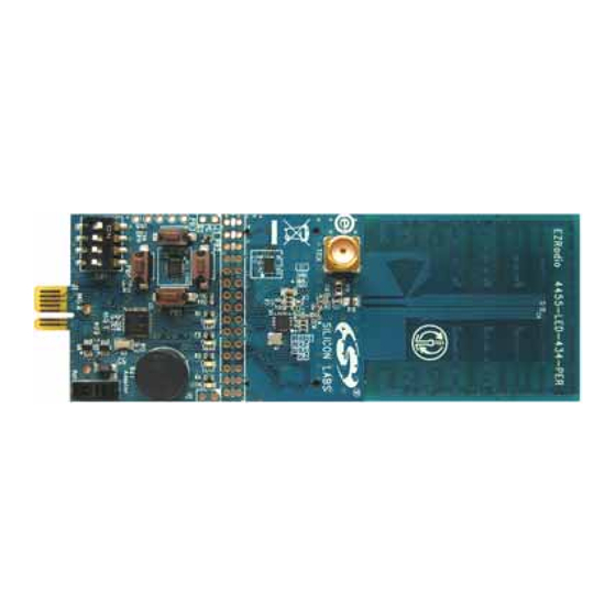
S i 4 3 5 5 / S i 445 5 P
1. Introduction
This document provides an overview of how to configure and control the following EZRadio
Si4455 transceiver
Si4355 receiver
The following code examples are covered in this programming guide:
How to set up a continuous wave (CW) transmission.
How to set up a pseudo random (PN9) transmission.
How to transmit in TX direct mode.
How to receive in RX direct mode (for BER measurement).
How to transmit a simple packet in Packet Handler mode.
How to receive a simple packet in Packet Handler mode.
How to implement bidirectional variable length packet based communication.
2. Hardware Options
The source code is provided for two different hardware platforms:
RFStick
Wireless Motherboard + RF Pico Board
A separate Silicon Labs IDE workspace is provided for each example on the two platforms.
2.1. The RFStick Platform
The RFStick is a basic demo system for the evaluation of the EZRadio chips. The board has two main parts, the
MCU part and the radio part. The MCU part of the board contains a Silicon Labs C8051F930 MCU and basic
human interface devices (four push-buttons, four LEDs, four switches and a buzzer). The radio part contains the
EZRadio chip, the matching circuit, and the antenna. The RF output is selectable via a 0 resistor between a PCB
antenna and an optional (unpopulated) 50 SMA output connector. The MCU is connected to the EZRadio chip
via an SPI bus and some other GPIOs (see Table 1). The RF section of the board can be broken off along a
perforation between the two rows of J3 and installed in the user's own hardware as a radio module by utilizing the
remaining row of J3.
Table 1 contains the signal connections between the EZRadio chip and the MCU:
Rev 0.4 11/14
R O G R A M M I N G
Figure 1. RFStick
Copyright © 2014 by Silicon Laboratories
G
U I D E
AN6 9 2
®
chips:
AN692
Advertisement

Related Manuals for Silicon Laboratories Si4355


Summary of Contents for Silicon Laboratories Si4355
- Page 1 J3 and installed in the user’s own hardware as a radio module by utilizing the remaining row of J3. Table 1 contains the signal connections between the EZRadio chip and the MCU: Rev 0.4 11/14 Copyright © 2014 by Silicon Laboratories AN692...
- Page 2 AN6 92 Table 1. Connections between the EZRadio Chip and the MCU Si4355, Si4455 RFStick C80C51F930 Pin Number Pin Name Pin Function Connections Signal Name Pin Name across J3 EP, 1, 6, 9 Ground 3–4 7, 8 Supply Voltage input 1–2...
- Page 3 AN 6 9 2 2.1.1. Setting up and Connecting the RFStick to a PC The power source of the board can be selected with the power-supply selector switch (S6). If S6 is in the Adapter position, supply voltage is provided by a Toolstick Base Adapter that is connected to the J1 PCB edge connector. If S6 is in the Battery position, the supply voltage is provided by two AAA batteries in the battery holder on the bottom side of the board.
- Page 4 AN6 92 2.2. The Wireless Motherboard Platform The Wireless Motherboard (WMB) platform is a demo and development platform for the EZRadio and EZRadioPRO radio ICs. It consists of a Wireless Motherboard and interchangeable MCU Pico Boards and RF Pico Boards. Figure 3.
- Page 5 AN 6 9 2 2.2.1. The Wireless Motherboard Figure 4. Wireless Motherboard The wireless motherboard contains four pushbuttons, four LEDs, and a buzzer as simple user interfaces. A graphical LCD displays menu items for range testing purposes and a potentiometer demonstrates analog capabilities of the MCU.
- Page 6 AN6 92 2.2.2. Power Scheme The power source of the platform can be selected with the power supply selector switch “SUPPLY SELECT” on the WMB board. If this switch is in the ”USB” position, supply voltage is provided by the PC that is connected to the ”J16”...
-
Page 7: Software Tools
3.1. Wireless Development Suite (WDS) The recommended starting point for Si4355/4455 development is the WDS. It can be downloaded from www.silabs.com.and can be installed on a PC. After connecting one of the hardware platforms described in this document to the PC, WDS is able to identify the connected board by reading the EBID memories. - Page 8 AN6 92 Figure 6. Device Configuration Options Rev 0.4...
- Page 9 AN 6 9 2 3.2. Silicon Labs IDE The Silicon Laboratories Integrated Development Environment (IDE) is a standard tool for program development for any Silicon Labs 8-bit MCUs, including the C8051F930 that is used on the hardware platforms described in this document.
- Page 10 To use the ToolStick Terminal in the IDE (above v4.60.00), follow these steps: 1. Open the Silabs IDE from the Start Programs Silicon Laboratories menu. 2. Go to the OptionsConnection Options menu and select the desired ToolStick Base Adapter from the drop down list.
- Page 11 4.1. Radio Hardware Interface The Si4355/Si4455 radios have several pins to interface to a host MCU. Four pins, SDI, SDO, SCLK, NSEL, are used to control the radio over the SPI bus. The user has access to an Application Programming Interface (API) via the SPI bus, which is described in section “4.2.
- Page 12 AN6 92 4.2. Application Programming Interface The programming interface allows the user to do the following: Send commands to the radio. Read status information. Set and get radio parameters. Handle the Transmit and Receive FIFOs. The API commands are listed in the following table: Table 4.
- Page 13 AN 6 9 2 The API properties are listed in Table 5. Table 5. List of the Radio API Properties Property Number Name Description Default Group 0x01 0x00 INT_CTL_ENABLE Interrupt enable property 0x04 0x01 0x01 INT_CTL_PH_ENABLE Packet handler interrupt enable property 0x00 0x01 0x02...
- Page 14 AN6 92 4.2.2. Checking that the Radio is Ready to Receive Commands 4.2.2.1. Software Polling Method To ensure the radio is ready to receive the next command, the host MCU must pull down the NSEL pin to monitor the status of CTS over the SPI port. The 0x44 command ID has to be sent, and eight clock pulses have to be generated, on the SCLK pin.
- Page 15 AN 6 9 2 4.2.3. Getting a Command Response from Radio Reading from the radio requires several steps to be followed. The host MCU should send a command with the address it requests to read. The radio holds the CTS while it retrieves the requested information. Once the CTS is set (0xFF), the host MCU can read the answer from the radio.
- Page 16 AN6 92 Figure 12. Monitor CTS and Read the Response on the SPI Bus Reading the response from the radio can be interrupted earlier. For example, if the host MCU asked for five bytes of response, it may read fewer bytes in one SPI transaction. As long as a new command is not sent, the radio keeps the response for the last request in the command buffer.
- Page 17 AN 6 9 2 4.2.4. Using Fast Response Registers There are several types of status information that can be read out from the radio faster. The FRR_CTL_x_MODE (where x can be A, B, C or D) properties define what status information is assigned to a given fast response register (FRR).
- Page 18 AN6 92 4.2.5. Write and Read the FIFOs There are two 64-byte FIFOs for RX and TX data in the Si4x55. To fill data into the transmit FIFO, the host MCU should pull the NSEL pin low and send the 0x66 Transmit FIFO Write command ID followed by the bytes to be filled into the FIFO.
- Page 19 AN 6 9 2 4.3. State Transitions of the EZRadio Devices Ready state is designed to give a fast transition time to TX or RX state with reasonable current consumption. In this mode the crystal oscillator remains enabled reducing the time required to switch to TX or RX mode by eliminating the crystal start-up time.
- Page 20 AN6 92 Table 6. Switching Times between Radio States State/Mode Response Time to Shutdown 15 ms 15 ms Sleep 440 μs 440 μs SPI Active 340 μs 340 μs Ready 126 μs 122 μs TX Tune 58 μs RX Tune 74 μs 138 μs 130 μs...
- Page 21 AN 6 9 2 Figure 19. Supply Current versus Time Diagram from Shutdown to Standby State Figure 20. Supply Current versus Time Diagram from Shutdown to TX State Rev 0.4...
- Page 22 AN6 92 Figure 21. Supply Current versus Time Diagram from Shutdown to RX State Rev 0.4...
- Page 23 AN 6 9 2 4.4. Radio Chip Waking Up Figure 22. Radio Wake Up Process Rev 0.4...
- Page 24 AN6 92 First the radio is in off state. After the SDN pin is pulled low, the radio wakes up and performs a Power on Reset, which takes a maximum of 5 ms until the chip is ready to receive commands on the SPI bus. GPIO1 pin goes high when the radio is ready for receiving SPI commands.
- Page 25 AN 6 9 2 4.5. EZConfig and Configuration Options Figure 23. Radio RF Initialization Process Rev 0.4...
- Page 26 AN6 92 EZConfig is a feature of Si4355/4455 that enables the customer to easily configure the radio by writing a single configuration array into the chip upon power up, using the EZCONFIG_SETUP command of the API. Generation of the configuration array content is automated with the Wireless Development Suite (WDS) that is provided free of charge by Silicon Labs.
-
Page 27: Example Projects
Silicon Laboratories IDE Used to open the preconfigured project files and manage the build process. Keil C51 v9.51+ compiler to use with the Silicon Laboratories IDE to manage build process. Silicon Labs Flash Programming Utility (optional) ... - Page 28 AN6 92 5.1.3. Software Layers In all of the sample projects, the layered software approach is followed. There is a distinct scope for each software module, and all modules can communicate through each other's API functions. The software modules are separated and focused to cover one specific task.
- Page 29 AN 6 9 2 Figure 25. Function Calls During the Radio Initialization 5.1.5. Directory Structure of the Example Project All sample source code has a common directory structure with separated source and project files to ease the understanding of the individual modules. For every sample project, the following directories and files can be found in the main directory: bin—Contains the SiLabs project files for Keil and SDCC compilers and the Makefile if the make tool is ...
- Page 30 AN6 92 5.2. Example Projects Description The general structure of an example project is shown in Figure 26. All the tasks are separated into two groups: the "Hardware Initialization" part and the "Main Process" part. The Host MCU related tasks initialize the physical interface between the radio and the controller unit, including the SPI lines (SCLK, SDI, SDO, NSEL) and general I/O ports (SDN, NIRQ).
- Page 31 AN 6 9 2 5.2.1. Continuous Wave (CW) and Pseudo Random (PN9) Transmission This example project demonstrates the EZConfig method for setting up the radio chip. In the main() function, there is only a function call to the vInitializeHW(). After the hardware and radio initialization, CW transmission starts. Since the MCU has no more tasks once the radio has been initialized, an empty infinite loop keeps running while in the cycle.
- Page 32 Sync Word Detect interrupt will work in this mode too. The direct mode is useful when already existing proprietary communication protocol has to be implemented using Silicon Laboratories radio transceivers. Figure 28. GPIO Connections between the Radio and the Host MCU (Direct TX) Figure 29.
- Page 33 AN 6 9 2 5.2.2.1. Direct Mode RX In RX direct mode, the RX Data and RX Clock can be programmed for direct (real-time) output to GPIO pins. The microcontroller may then process the RX data without using the FIFO or packet handler functions of the RFIC. The GPIOs of the radio used for the RX_DATA and RX_DATA_CLK output can be changed without generating a new configuration file again.
- Page 34 AN6 92 5.2.3. Transmission of a Simple Packet in Packet Handler Mode This example project demonstrates the usage of the radio chip in fixed packet length mode and utilizes the advantages of the Packet Handler feature. This example project uses the radio to transmit the “BUTTONx” packets, where “x” value can be “1–4” depending on which button was pressed.
- Page 35 AN 6 9 2 Figure 32. Transmission Flowchart Rev 0.4...
- Page 36 AN6 92 5.2.4. Reception of a Simple Packet in Packet Handler Mode This example project demonstrates the usage of the radio chip for reception in fixed packet length mode and utilizes the advantages of the Packet Handler feature. This project uses the Human Machine Interface software module that is used in the transmitter side project as well.
- Page 37 AN 6 9 2 5.2.4.1. Key Fob Compatibility with the Si4x55 RF Receiver This section is intended to describe the compatibility between the Si4x55 RF IC working as a receiver and different key fobs working as transmitters. Silicon Labs provides two types of demo kits containing key fobs with different packet structures.
- Page 38 AN6 92 Function No change Sets output logical low (LED is OFF) Sets output logical high (LED is ON) Packet type #2 The structure of the packet: Preamble Sync Word Chip Id Status Packet Count 13 byte 2 byte 4 byte 1 byte 2 byte 2 byte...
- Page 39 AN 6 9 2 Figure 33. Reception Flowchart Rev 0.4...
- Page 40 AN6 92 5.2.5. Bidirectional Variable Length Packet Based Communication This example project uses the radio both in receive and transmit mode in order to establish a two-way link between two demo boards. At startup, the radio is initialized according to the settings in radio_config.h file. The Packet Handler in the radio is configured to receive variable length packets from the transmitter.
- Page 41 AN 6 9 2 Figure 34. Bidirectional Variable Packet Example Project Flowchart Rev 0.4...
- Page 42 AN6 92 5.2.6. Continuous Transmission of Custom Amount of Standard Packets The purpose of the standard packet transmission example code is to demonstrate how the radio can send packets in FIFO mode continuously. If the first button is pressed on the Wireless Motherboard then the host MCU will load the pre-defined content, namely “BUTTON1”...
- Page 43 AN 6 9 2 Figure 36. General Usage of the Continuous Transmission In order to calculate the minimum number of packets to be transmitted, it is necessary to know how the different time periods, such as the “Transmit Time”, the “RX Time” and “Sleep Time” relate to one another in the worst case scenario.
- Page 44 AN6 92 5.2.7. Host MCU Implemented Low Duty Cycle Figure 37. Host MCU Implemented Low Duty Cycle Flowchart Rev 0.4...
- Page 45 AN 6 9 2 The basic operation of low duty cycle mode is shown in Figure 37. The host MCU periodically wakes up the radio chip to work in reception mode. If a valid preamble is not detected within the "LDC_CONFIG_AWAKE_TIME_MS" time, the host MCU forces the receiver to "LDC_State_Sleep State"...
- Page 46 AN6 92 5.2.8. Long Packet Transmission Applications requiring transmission of packets longer than the TX FIFO size (64 bytes) may use the long packet feature of the radio. In this case, TX FIFO Almost Empty Interrupt should be monitored for proper timing to fill the TX FIFO.
- Page 47 AN 6 9 2 Figure 41. Long Packet Transmission Flowchart Rev 0.4...
- Page 48 AN6 92 Figure 42. Long Packet RX Flowchart Rev 0.4...
- Page 49 AN 6 9 2 5.2.10. Empty Project The empty project is created to help users start writing their custom firmware. The project follows the convention for directory structure introduced in the example projects. It contains driver modules for the radio and MCU peripherals as well as a default MCU initialization procedure.
- Page 50 AN6 92 5.3. Radio Driver The radio driver module resides in a low-level driver software layer. It is intended to provide a more user-friendly and easy-to-use API to the radio functionality. The radio driver contains API functions and macro definitions for all radio commands and constants can be found in the EZRadio API documentation.
- Page 51 AN 6 9 2 5.3.2. Size Optimization of the Radio Driver To optimize the code size of the common software modules and the example project, software switches are introduced in the radio driver. By activating the switches, new functions can be added to the radio driver. If none of the radio driver switches are defined at the beginning of the 'bsp.h' header file, then only the basic features are used;...
- Page 52 AN6 92 5.3.3. Minimal Radio Driver void si4455_reset(void); Function Name: This functions is used to reset the si4455 radio by applying shutdown and releasing it. Description: After this function, si4455_boot should be called. You can check if POR has com- pleted by waiting 5 ms or by polling GPIO 0, 2, or 3.
- Page 53 AN 6 9 2 void si4455_start_rx(U8 CHANNEL, U8 CONDITION, U16 RX_LEN, U8 NEX- Function Name: T_STATE1, U8 NEXT_STATE2, U8 NEXT_STATE3); Sends START_RX command to the radio. Description: CHANNEL : Channel number. Input Parameter(s): CONDITION : Start RX condition. RX_LEN : Payload length (exclude the PH generated CRC). NEXT_STATE1 : Next state when Preamble Timeout occurs.
- Page 54 AN6 92 void si4455_change_state(U8 NEXT_STATE1); Function Name: Issue a change state command to the radio. Description: NEXT_STATE1 : Next state Input Parameter(s): None Return Value: 5.3.4. Extended Radio Driver void si4455_nop(void) Function Name: Sends NOP command to the radio. Can be used to maintain SPI communication. Description: None Return Value:...
- Page 55 AN 6 9 2 void si4455_get_property(U8 GROUP, U8 NUM_PROPS, U8 START_PROP) Function Name: Get property values from the radio. Reads them into Si4455Cmd union. Description: GROUP : Property group number. Input Parameter(s): NUM_PROPS : Number of properties to be read. START_PROP : Starting sub-property number.
- Page 56 AN6 92 void si4455_frr_d_read(U8 respByteCount) Function Name: Returns the fast response registers (FRR) starting with FRR_D into Si4455Cmd Description: union. respByteCount : Data length to be read. Input Parameter(s): None Return Value: void si4455_read_cmd_buffer(void); Function Name: Returns Clear to Send (CTS) value and the result of the previous command. Description: None Return Value:...
- Page 57 AN 6 9 2 void si4455_get_chip_status( U8 CHIP_CLR_PEND ); Function Name: Returns the interrupt status of the Chip Interrupt Group into Si4455Cmd union. Description: Optionally clears pending flags. CHIP_CLR_PEND : Chip State pending flags to clear. Input Parameter(s): None Return Value: Rev 0.4...
- Page 58 AN6 92 5.4. Common Software Modules In the modules hierarchy, the common software modules (CSM) are located between the application and the hardware layers.The CSM are a set of interfaces that enable control of various peripherals on modular HW platforms. Registers can be initialized with pre-configured settings and peripherals can be enabled to start/stop their own processing.
- Page 59 AN 6 9 2 5.4.2. Input Output Control Module The IO control-related source files, called 'control_IO.h' and 'control_IO.c', can be found in the /src/drivers/ folder. The module handles the port initializations for the physical HW platform, e.g., LEDs, push-buttons, buzzer. It can set the state of the LEDs and read the status of the selected push-buttons.
- Page 60 AN6 92 5.4.3. Timer Peripheral Module The timer related source files, called ' timer.h' and 'timer.c', can be found in the /src/drivers/ folder. The module handles two 16-bit timers, timer2 and timer3. The most accurate timing interval can be calculated from the frequency of the system clock which is generally 24.5 MHz.
- Page 61 AN 6 9 2 5.4.4. Programmable Counter Array Module The PCA related source files, called 'pca.h' and 'pca.c', can be found in the /src/driver/ folder. The module initializes the PCA to create beeping sounds on the buzzer. The time-base source of the PCA counter can be selected. Interrupts can be generated when the lower byte of the counter overflows.
- Page 62 AN6 92 void vSpi_WriteDataSpi0(U8 biDataInLength, U8 *pabiDataIn) Function Name: This function is used to send data over SPI0 no response expected. Description: biDataInLength : The length of the data. Input Parameter(s): *pabiDataIn : Pointer to the first element of the data. None Return Value: void vSpi_WriteDataSpi1(U8 biDataInLength, U8 *pabiDataIn)
- Page 63 AN 6 9 2 void vSpi_DisableSpi0(void) Function Name: This function is used to disable SPI0 and disconnect from XBAR. Description: None Return Value: void vSpi_DisableSpi1(void) Function Name: This function is used to disable SPI1 and disconnect from XBAR. Description: None Return Value: void vSpi_ClearNselSpi0(U8 biSelectDevice) Function Name:...
- Page 64 AN6 92 Function Name: U8 bSpi_ReadByteBitbangSpi0(void) This function is used to read one byte from SPI0 using bitbang method. Description: Read byte Return Value: Function Name: U8 bSpi_ReadByteBitbangSpi1(void) This function is used to read one byte from SPI1 using bitbang method. Description: Read byte Return Value:...
- Page 65 AN 6 9 2 void vHmi_ChangeLedState(eHmi_Leds qiLed, eHmi_LedStates qiLedState) Function Name: This function is used to change state of selected LED. Description: qiLed : LED to change its state Input Parameter(s): qiLedState : New state of qiLed None Return Value: void vHmi_ChangeAllLedState(eHmi_LedStates qiLedState) Function Name: This function is used to change state of all LEDs.
- Page 66 AN6 92 BIT gHmi_IsPbUnHandled(void) Function Name: This function is used to check if there are unhandled push-buttons events. Description: True if there is unhandled push-button event. Return Value: U8 bHmi_PbGetLastButton(U16 *woPbPushTime) Function Name: This function is used to read last pushed button(s), push track holder is erased if but- Description: ton(s) were already released.
- Page 67 AN 6 9 2 void vHmi_ChangeBuzzState(eHmi_BuzzStates qiBuzzState) Function Name: This function is used to change the state of the buzzer. Description: qiBuzzState : New state of the buzzer Input Parameter(s): None Return Value: void vHmi_BuzzHandler(void) Function Name: This function is used to handle buzzer management. Description: None Return Value:...
- Page 68 AN6 92 5.4.8. Size Optimization of the Common Software Modules To optimize the code size of the common software modules as well as the example source codes, software switches must be introduced in almost every module. By enabling these switches, new functions can be added to the whole project to compile.
- Page 69 AN 6 9 2 Table 11 shows the comparison between the modules' sizes: Table 11. Size Comparison of Common Software Module Common Software Module Code Size [Byte] Size Optimization Module Minimal Driver Extended Driver Control IO Not supported Timer Not supported 1295 UART Rev 0.4...
- Page 70 The products must not be used within any Life Support System without the specific written consent of Silicon Laboratories. A "Life Support System" is any product or system intended to support or sustain life and/or health, which, if it fails, can be reasonably expected to result in significant personal injury or death.
Need help?
Do you have a question about the Si4355 and is the answer not in the manual?
Questions and answers