Fibocom L860-GL Hardware User Manual
Hide thumbs
Also See for L860-GL:
- Hardware user manual (55 pages) ,
- At command user manual (254 pages)
Table of Contents
Advertisement
Quick Links
Advertisement
Table of Contents

Subscribe to Our Youtube Channel
Related Manuals for Fibocom L860-GL


Summary of Contents for Fibocom L860-GL
- Page 1 L860-GL Hardware User Manual Version:1.0.2 Update date:July 19rd, 2018...
- Page 2 Copyright Copyright © 2018 Fibocom Wireless Inc. All rights reserved. Copyright © 2018 Fibocom Wireless Inc. All rights reserved. Without the prior written permission of the copyright holder, any company or individual is prohibited to excerpt, prior written permission of the copyright holder, any company or individual is prohibited to excerpt, prior written permission of the copyright holder, any company or individual is prohibited to excerpt, copy any part of or the entire document, or distribute the document in any form.
- Page 3 B unintentional radiator requirements after the module is installed and operational. Reproduction forbidden without Fibocom Wireless Inc. written authorization Reproduction forbidden without Fibocom Wireless Inc. written authorization - All Rights Reserved. FIBOCOM_L860-GL Hardware User Manual Page 4 of 55...
- Page 4 RF module in the user’s manual of the end product which integrates this module. The end user manual shall include all required regulatory information/warning as show in this manual. Reproduction forbidden without without Fibocom Wireless Inc. written authorization - All Rights Rights Reserved. L860-GL Hardware User Manual...
- Page 5 Trademark The trademark is registered and owned by Fibocom Wireless Inc. The trademark is registered and owned by Fibocom Wireless Inc. The trademark is registered and owned by Fibocom Wireless Inc. Version Record Version Record Version Update date Remark Remark V1.0.0...
-
Page 6: Table Of Contents
..............31 3.4.2.1 USB Interface Definition Interface Definition ..........................31 3.4.2.2 USB2.0 Interface USB2.0 Interface Application ..............Reproduction forbidden without without Fibocom Wireless Inc. written authorization - All Rights Rights Reserved. L860-GL Hardware User Manual Page 6 of 53... - Page 7 Dimension of Structure Structure ..............................49 ............50 M.2 Interface Model ........................................50 M.2 Connector ..........................Reproduction forbidden without without Fibocom Wireless Inc. written authorization - All Rights Rights Reserved. L860-GL Hardware User Manual Page 7 of 53...
- Page 8 Packing ..........................................51 5.6.1 Tray Package......................................51 ..............53 5.6.2 Tray size ..........................Reproduction forbidden without without Fibocom Wireless Inc. written authorization - All Rights Rights Reserved. L860-GL Hardware User Manual Page 8 of 53...
-
Page 9: Foreword
The document describes the electrical characteristics, RF performance, dimensions and application environment, etc. of L860-GL (hereinafter referred to as L860). With the assistance of the document and other instr GL (hereinafter referred to as L860). With the assistance of the document and other instr GL (hereinafter referred to as L860). -
Page 10: Overview
Support 4x4 MIMO Support 4x4 MIMO Dual SIM, 3V/1.8V Dual SIM, 3V/1.8V Function PCIe 2.0 X1 Interface USB 2.0 Reproduction forbidden without without Fibocom Wireless Inc. written authorization - All Rights Rights Reserved. L860-GL Hardware User Manual Page 10 of... -
Page 11: Ca Combinations
7+8, 20, 28, 32, 46 12+30, 66 13+46, 66 Inter-band 14+30, 66 19+21, 42 20+32 21+42 25+26, 41, 46 26+41 29+30, 66 Reproduction forbidden without without Fibocom Wireless Inc. written authorization - All Rights Rights Reserved. L860-GL Hardware User Manual Page 10 of 53... - Page 12 2 intra-band(contiguous) plus 2 band(contiguous) plus 2 1+3+3+7+7, 3+3+7+7+28, 2+46+46+46+46, 1+3+3+7+7, 3+3+7+7+28, 2+46+46+46+46, intra-band(contiguous) plus band(contiguous) plus 46+46+46+46+66 inter-band Reproduction forbidden without without Fibocom Wireless Inc. written authorization - All Rights Rights Reserved. L860-GL Hardware User Manual Page 11 of 53...
-
Page 13: Application Framework Application Framework
The hardware block diagram in Figure 2-2 shows the main hardware functions of L860 module, including base hardware functions of L860 module, including base band and RF functions. Baseband contains the followings: Reproduction forbidden without without Fibocom Wireless Inc. written authorization - All Rights Rights Reserved. L860-GL Hardware User Manual Page 12 of 53... -
Page 14: Antenna Configuration
Diversity & GNSS ANT Diversity & GNSS ANT All supported bands and GNSS receive All supported bands and GNSS receive Reproduction forbidden without without Fibocom Wireless Inc. written authorization - All Rights Rights Reserved. L860-GL Hardware User Manual Page 13 of 53... -
Page 15: Application Interface
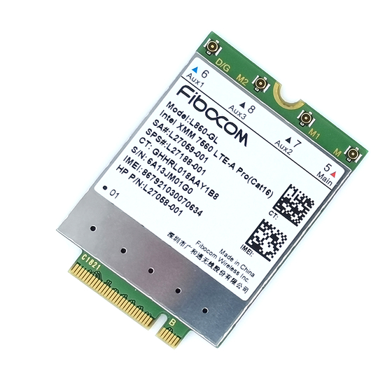
Pin “Notch” represents the gap of the gold fingers. Pin “Notch” represents the gap of the gold fingers. Reproduction forbidden without without Fibocom Wireless Inc. written authorization - All Rights Rights Reserved. L860-GL Hardware User Manual Page 14 of 53... -
Page 16: Pin Definition
CMOS 1.8V Reserved WOWWAN# Wake up host, Reserved CMOS 1.8V I2S_TX I2S Serial transmit data, Reserved CMOS 1.8V Reproduction forbidden without without Fibocom Wireless Inc. written authorization - All Rights Rights Reserved. L860-GL Hardware User Manual Page 15 of 53... - Page 17 CMOS 3.3V default. If module went into core dump, it default. If module went into core dump, it Reproduction forbidden without without Fibocom Wireless Inc. written authorization - All Rights Rights Reserved. L860-GL Hardware User Manual Page 16 of 53...
- Page 18 WiFi/BT modules, based on BT-SIG COEX_RXD CMOS 1.8V coexistence protocol. UART receive signal(WWAN module side), Reserved signal(WWAN module side), Reserved Reproduction forbidden without without Fibocom Wireless Inc. written authorization - All Rights Rights Reserved. L860-GL Hardware User Manual Page 17 of 53...
- Page 19 PO: Power Output Note: The unused pins can be left floating. The unused pins can be left floating. Reproduction forbidden without without Fibocom Wireless Inc. written authorization - All Rights Rights Reserved. L860-GL Hardware User Manual Page 18 of 53...
-
Page 20: Power Supply
The L860 module should be powered through the +3.3V pins, and the power supply design is shown in Figure 3-2: Figure 3-2 Power Supply Design Reproduction forbidden without without Fibocom Wireless Inc. written authorization - All Rights Rights Reserved. L860-GL Hardware User Manual... - Page 21 The L860 module 1.8V logic level definition as shown in the following table: logic level definition as shown in the following table: Reproduction forbidden wit without Fibocom Wireless Inc. written authorization - All Rights Rights Reserved. L860-GL Hardware User Manual...
-
Page 22: Power Consumption Consumption
LTE FDD Data call Band 1 @+23dBm LTE FDD Data call Band 2 @+23dBm LTE FDD LTE-RMS LTE FDD Data call Band 3 @+23dBm Reproduction forbidden wit without Fibocom Wireless Inc. written authorization - All Rights Rights Reserved. L860-GL Hardware User Manual Page 21 of 53... - Page 23 LTE TDD Data call Band 40 @+23dBm LTE TDD LTE TDD Data call Band 41 @+23dBm LTE TDD Data call Band 42 @+23dBm Reproduction forbidden wit without Fibocom Wireless Inc. written authorization - All Rights Rights Reserved. L860-GL Hardware User Manual Page 22 of 53...
-
Page 24: Control Signal
If module went into core dump, 3.3V it will reset whole module, not only it will reset whole module, not only Reproduction forbidden wit without Fibocom Wireless Inc. written authorization - All Rights Rights Reserved. L860-GL Hardware User Manual Page 23 of 53... -
Page 25: Module Start-Up
Figure 3-5: Figure 3 Figure 3-5 Timing Control for Start-up Index Minimum Typical Notes Reproduction forbidden wit without Fibocom Wireless Inc. written authorization - All Rights Rights Reserved. L860-GL Hardware User Manual Page 24 of 53... -
Page 26: Module Shutdown
RESET# should asserted before FULL_CARD_POWER_OFF# asserted before FULL_CARD_POWER_OFF# 30ms off1 30ms PERST# should asserted after RESET# off2 off1 Reproduction forbidden wit without Fibocom Wireless Inc. written authorization - All Rights Rights Reserved. L860-GL Hardware User Manual Page 25 of 53... -
Page 27: Module Reset
Host may assert FULL_CARD_POWER_OFF# high when system restarting, module reset timing is shown in the Figure 3-9; Figure 3- 8 Reset control timing1 Reproduction forbidden wit without Fibocom Wireless Inc. written authorization - All Rights Rights Reserved. L860-GL Hardware User Manual Page 26 of 53... -
Page 28: Pcie Reset
Module supports PCIe goes in to D3cold L2 state in Win10 system. The D0->D3cold L2@S0/S0ix/S3 >D3cold L2@S0/S0ix/S3 ->D0 timing is shown in figure 3- -10: Figure 3- 10 PCIe reset timing Reproduction forbidden wit without Fibocom Wireless Inc. written authorization - All Rights Rights Reserved. L860-GL Hardware User Manual Page 27 of 53... -
Page 29: Pcie & Usb
CMOS 3.3V module went into coredump, it will reset whole will reset whole module, not only PCIe interface. Reproduction forbidden wit without Fibocom Wireless Inc. written authorization - All Rights Rights Reserved. L860-GL Hardware User Manual Page 28 of 53... -
Page 30: Pcie Interface Pcie Interface Application
The impedance of differential signal pair lines is recommended to be 100 ohm, and can be controlled to 80~120 ohm in accordance with PCIe 120 ohm in accordance with PCIe protocol; Reproduction forbidden wit without Fibocom Wireless Inc. written authorization - All Rights Rights Reserved. L860-GL Hardware User Manual Page 29 of 53... - Page 31 Reproduction forbidden without without Fibocom Wireless Inc. written authorization - All Rights Rights Reserved. L860-GL Hardware User Manual...
-
Page 32: Usb Interface
USB_D- and USB_D+ signal signal lines should be parallel and have the equal length, length, the right angle routing Reproduction forbidden without without Fibocom Wireless Inc. written authorization - All Rights Rights Reserved. L860-GL Hardware User Manual Page 31 of 53... -
Page 33: Usim Interface
SIM card is detached. Reproduction forbidden without without Fibocom Wireless Inc. written authorization - All Rights Rights Reserved. L860-GL Hardware User Manual Page 32 of 53... -
Page 34: Usim Interface Circuit
When the SIM card is detached, it connects an open circuit between CD and SW pins, and When the SIM card is detached, it connects an open circuit between CD and SW pins, and drives the Reproduction forbidden without without Fibocom Wireless Inc. written authorization - All Rights Rights Reserved. L860-GL Hardware User Manual... -
Page 35: Usim Hot-Plugging Plugging
DC/DC power supply, clock signal lines, and other strong interference DC/DC power supply, clock signal lines, and other strong interference sources. Reproduction forbidden without without Fibocom Wireless Inc. written authorization - All Rights Rights Reserved. L860-GL Hardware User Manual Page 34 of 53... -
Page 36: Status Indicator
LED current-limiting resistor is selected according to the driving voltage and the limiting resistor is selected according to the driving voltage and the Reproduction forbidden without without Fibocom Wireless Inc. written authorization - All Rights Rights Reserved. L860-GL Hardware User Manual... -
Page 37: Interrupt Control
Lower the maximum emission power to the threshold value of the module. Lower the maximum emission power to the threshold value of the module. Reproduction forbidden without without Fibocom Wireless Inc. written authorization - All Rights Rights Reserved. L860-GL Hardware User Manual... -
Page 38: Ant_Config
The L860 module provides four configuration pins for the configuration as the WWAN-PCIe, USB3.0 type M.2 PCIe, USB3.0 type M.2 Reproduction forbidden without without Fibocom Wireless Inc. written authorization - All Rights Rights Reserved. L860-GL Hardware User Manual Page 37 of 53... -
Page 39: Other Interfaces
3.10 Other Interfaces Interfaces The module does not support other interfaces yet. The module does not support other interfaces yet. Reproduction forbidden without without Fibocom Wireless Inc. written authorization - All Rights Rights Reserved. L860-GL Hardware User Manual Page 38 of 53... -
Page 40: Radio Frequency
2*2*0.6m. The connector dimension is shown as following picture: the connector size is 2*2*0.6m. The connector dimension is shown as following picture: Reproduction forbidden without without Fibocom Wireless Inc. written authorization - All Rights Rights Reserved. L860-GL Hardware User Manual... - Page 41 0.81mm coaxial antenna connected to the RF connector chematic diagram of 0.81mm coaxial antenna connected to the RF connector Reproduction forbidden without without Fibocom Wireless Inc. written authorization - All Rights Rights Reserved. L860-GL Hardware User Manual...
-
Page 42: Operating Band
Band 40 2300MHz LTE TDD 2300 2300 - 2400 Band 41 2500MHZ LTE TDD 2496 2496 - 2690 Reproduction forbidden without without Fibocom Wireless Inc. written authorization - All Rights Rights Reserved. L860-GL Hardware User Manual Page 41 of 53... -
Page 43: Transmitting Power
10MHz Bandwidth, 1 RB 10MHz Bandwidth, 1 RB 23±2.7 23±1 Band 20 10MHz Bandwidth, 1 RB 10MHz Bandwidth, 1 RB Reproduction forbidden without without Fibocom Wireless Inc. written authorization - All Rights Rights Reserved. L860-GL Hardware User Manual Page 42 of 53... -
Page 44: Receiver Sensitivity
LTE FDD Band 4 -96.3 -101.5 10MHz Bandwidth Band 5 -94.3 -103.1 10MHz Bandwidth Band 7 -94.3 10MHz Bandwidth Reproduction forbidden without without Fibocom Wireless Inc. written authorization - All Rights Rights Reserved. L860-GL Hardware User Manual Page 43 of 53... -
Page 45: Four Antenna Receiver Receiver Sensitivity
Some middle/high bands support four antenna, the receiver sensitivity for some middle/high bands of L860 module Some middle/high bands support four antenna, the receiver sensitivity for some middle/high bands of L860 module Reproduction forbidden without without Fibocom Wireless Inc. written authorization - All Rights Rights Reserved. L860-GL Hardware User Manual... -
Page 46: Gnss
Power GPS Sleep GPS Sleep GLONASS Sleep GLONASS Sleep BeiDou Sleep BeiDou Sleep Cold start Cold start TTFF Reproduction forbidden without without Fibocom Wireless Inc. written authorization - All Rights Rights Reserved. L860-GL Hardware User Manual Page 45 of 53... -
Page 47: Antenna Design
WCDMA band 8(900) : 80 MHz WCDMA band 8(900) : 80 MHz Bandwidth(LTE) LTE band 1(2100): 250 MHz Reproduction forbidden without without Fibocom Wireless Inc. written authorization - All Rights Rights Reserved. L860-GL Hardware User Manual Page 46 of 53... - Page 48 > 28 dBm average power WCDMA & LTE > 28 dBm average power WCDMA & LTE Recommended standing-wave ratio ≤ 2:1 ≤ 2:1 Reproduction forbidden without without Fibocom Wireless Inc. written authorization - All Rights Rights Reserved. L860-GL Hardware User Manual Page 47 of 53...
- Page 49 ANT on B30 suggestion: Peak gain<0dBi, for FCC EIRP requirement, Efficient>50% for carrier TRP requirement, Efficient>50% for carrier TRP requirement. If integrator doesn't follow the instruction, Fibocom doesn't take the responsibility. requirement. If integrator doesn't follow the instruction, Fibocom doesn't take the responsibility.
-
Page 50: Structure Specification
The structural dimension of the L860 module is shown in Figure 5 The structural dimension of the L860 module is shown in Figure 5-2: Figure 5-2 Dimension of Structure Reproduction forbidden without without Fibocom Wireless Inc. written authorization - All Rights Rights Reserved. L860-GL Hardware User Manual Page 49 of 53... -
Page 51: Interface Model
P001A as shown in Figure 5-3. The package of connector, please refer to the 3. The package of connector, please refer to the specification. Reproduction forbidden without without Fibocom Wireless Inc. written authorization - All Rights Rights Reserved. L860-GL Hardware User Manual Page 50 of 53... - Page 52 5 boxes in each case. Tray packaging process is shown in Figure 5 each box and 5 boxes in each case. Tray packaging process is shown in Figure 5-4: Reproduction forbidden without without Fibocom Wireless Inc. written authorization - All Rights Rights Reserved. L860-GL Hardware User Manual...
- Page 53 Figure 5-4 Tray Packaging Process Reproduction forbidden without without Fibocom Wireless Inc. written authorization - All Rights Rights Reserved. L860-GL Hardware User Manual Page 52 of 53...
- Page 54 Figure 5-5 Tray Size (Unit: mm) ITEM DIM(Unit: mm) 315.0±2.0 170.0±2.0 6.5±0.3 0.8±0.1 43.0±0.3 31.0±0.3 79.0±0.2 60.0±0.2 180.0±0.2 60.0±0.2 40.0±0.2 Reproduction forbidden without without Fibocom Wireless Inc. written authorization - All Rights Rights Reserved. L860-GL Hardware User Manual Page 53 of 53...
Need help?
Do you have a question about the L860-GL and is the answer not in the manual?
Questions and answers