Table of Contents
Advertisement
Quick Links
Advertisement
Table of Contents

Related Manuals for Fibocom L830-EA M.2


Summary of Contents for Fibocom L830-EA M.2
- Page 1 L830-EA M.2 Module Hardware User Manual Version:V1.0.3 Date:2015.09.19...
- Page 2 Unless otherwise specified, the document only serves as the user guide. All the statements, information and suggestions contained in the document do not constitute any explicit or implicit guarantee. Trademark The trademark is registered and owned by Fibocom Wireless Inc. Versions Version Date Remarks V1.0.0...
- Page 3 Applicability Table Type Note L830-EA The difference of L830-EA M.2 wireless module as listed below: Model No. LTE FDD WCDMA GSM/GPRS/EDGE Band Band L830-EA 850/900/1800/1900MHz 1,2,4,5,6,8 1,2,3,4,5,7,8,9,13,17,18,19,20,26,29 Page 3 of 45 L830-EA M.2 Module Hardware User Manual...
-
Page 4: Table Of Contents
5.2.2 RESET Signal..........................26 5.3 Status Indicating Signal..........................27 5.3.1 Status Indicating Pin........................27 5.4 USB /SSIC Interface...........................28 5.4.1 USB Interface........................... 28 5.4.2 USB SSIC Interface.........................29 5.5 USIM Interface.............................29 5.5.1 USIM Pins............................29 Page 4 of 45 L830-EA M.2 Module Hardware User Manual... - Page 5 6.1 Electrical Features............................39 6.2 Environmental Features..........................40 7 RF Interface................................41 7.1 Operating Frequency Band........................41 7.2 Receiving Sensitivity...........................42 7.3 GNSS................................43 7.4 RF PCB Design............................43 7.4.1 Wiring Principle..........................43 Page 5 of 45 L830-EA M.2 Module Hardware User Manual...
- Page 6 7.4.2 Impedance Design...........................43 7.5 Antenna Design............................44 7.5.1 Main Antenna Design Requirements................... 44 Page 6 of 45 L830-EA M.2 Module Hardware User Manual...
-
Page 7: Foreword
1.1 Introduction The document describes the electrical characteristics, RF performance, dimensions and application environment, etc. of L830-EA M.2 wireless modules. With the assistance of the document and other instructions, developers can quickly understand the performance of L830-EA M.2 wireless modules and develop products. - Page 8 3GPP TS 34.122 V5.7.0: Technical Specification Group Radio Access Network; Radio transmission and reception (TDD) 3GPP TS 45.005 9.4.0: Digital cellular telecommunications system (Phase 2+); Radio transmission and reception Page 8 of 45 L830-EA M.2 Module Hardware User Manual...
-
Page 9: Product Overview
2 Product Overview 2.1 Description L830-EA M.2 modules are highly integrated 4G wireless modules, supports 3 modes 16 bands that including the main 4G/3G/2G modes (LTE FDD/ WCDMA/ /GSM) and with wide bands, but not TDD mode in China. These bands support the main operators of Europe and North America and the cellular network of parts of the Asia . - Page 10 Coding Scheme MCS1~4 UMTS(14.4kbps),GSM(9.6kbps) USSD Support MO / MT Text and PDU modes Cell broadcast Audio not supported yet Character Set IRA,GSM,UCS2,HEX FIBOCOM proprietary AT commands AT Commands GSM 07.05 GSM 07.07 Page 10 of 45 L830-EA M.2 Module Hardware User Manual...
- Page 11 3. Assessment of compliance of the product with the requirements relating to the Radio and Telecommunication Terminal Equipment Directive (EC Directive 1999/5/EC) was performed by PHOENIX TESTLAB (Notified Body No.0700), Page 11 of 45 L830-EA M.2 Module Hardware User Manual...
- Page 12 20cm (8 inches) during normal operation. IMPORTANT NOTE: This module is intended for OEM integrator. The OEM integrator is still responsible for the FCC Page 12 of 45 L830-EA M.2 Module Hardware User Manual...
- Page 13 Operation is subject to the following two conditions: (1) this device may not cause harmful interference and (2) this device must accept any interference received, including interference that may cause undesired operation. Page 13 of 45 L830-EA M.2 Module Hardware User Manual...
-
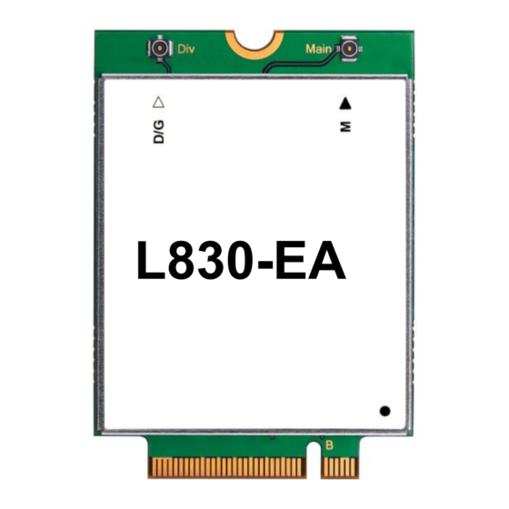
Page 14: Appearance
2.3 Appearance The product appearance of L830-EA M.2 wireless module is shown as below: Top View: L830-EA Figure 2- 1 Top View Bottom view: Figure 2- 2 Bottom View Page 14 of 45 L830-EA M.2 Module Hardware User Manual... -
Page 15: Structure
3 Structure 3.1 Dimension Diagram of Structure Figure 3- 1 Dimension Diagram of Structure Page 15 of 45 L830-EA M.2 Module Hardware User Manual... -
Page 16: Application Interface Description
3.2 Application Interface Description L830-EA M.2 module uses 75-pin gold fingers as the external interface, the size of the module please refer to the section 3.1.As shown in Figure 4-2, L830-EA M.2 module uses the 75-pin fingers interface ( 67 pins are the signal interface and 8 pins are notch) .About the naming rules of M.2, L830-EA adopts the Type 3042-S3-B (30mmx42mm,the maximum thickness of element layer of Top surface is 1.5mm , the... -
Page 17: Connector
Recommend to use the M.2 connector from LOTES, the type is APCI0026-P001A, the package of connector design please refer to the relevant specifications. As shown in Figure 3-2: Figure 3- 2 APCI0026-P001A M.2 connector dimension Page 17 of 45 L830-EA M.2 Module Hardware User Manual... -
Page 18: Hardware Introduction
SSIC-RXN UIM_DATA UIM_CLK SSIC-TXP UIM_RESET SSIC-TXN I2S_WA W_DISABLE2# I2S_TX WOWWAN# I2S_RX CONFIG_0 I2S_CLK Notch Notch Notch Notch Notch Notch Notch Notch LED1#(3.3V) USB D- W_DISABLE1#(3.3V) USB D+ FUL_CARD_POWER_OFF#(1.8V) +3.3V +3.3V Page 18 of 45 L830-EA M.2 Module Hardware User Manual... -
Page 19: Description Of Pins
CONFIG_3 Figure 4-2 Pin Diagram (TOP View) 4.1.2 Description of Pins Pins of L830-EA M.2 modules are described in the table below: Reset Idle Pin# PIN Name Description Value Value The internal connected with GND, CONFIG_3 L830-EA M.2 module shall configure as the WWAN-SSIC0 interface type. - Page 20 USB SSIC Receive data minus SIM card power supply output, UIM_PWR 1.8V/3.0V SSIC-RXP USB SSIC Receive data plus I2C serial data clock signal, GNSS_SCL internal 4.7K pull-up resistor, CMOS 1.8V Page 20 of 45 L830-EA M.2 Module Hardware User Manual...
- Page 21 CMOS 1.8V. (Not supported yet) Tunable antenna control signal, MIPI ANTCTL1 RFFE SDATA, CMOS 1.8V . (Not supported yet) Tunable antenna control signal, MIPI ANTCTL2 RFFE SCLK, CMOS 1.8V. (Not supported yet) Page 21 of 45 L830-EA M.2 Module Hardware User Manual...
- Page 22 L830-EA M.2 module configure as the WWAN-SSIC0 interface type. PI:Power Input H:High Voltage Level L:Low Voltage Level PD:Pull-Down PU:Pull-Up T:Tristate OD:Open Drain PP:Push-Pull Note : the unused pins can NC directly while designing. Page 22 of 45 L830-EA M.2 Module Hardware User Manual...
-
Page 23: Hardware Interface
5 Hardware Interface 5.1 Power Interface 5.1.1 Power Supply L830-EA M.2 modules require 3.135V ~ 4.4V direct current power supply, which can provide the maximum GSM emission current of 2A. Input power supply requirements: Parameter Minimum Value Recommended Value Maximum Value Unit +3.3V... -
Page 24: Power On/Off And Reset Signal
0.7* VSD2_1V8 1.8865 -0.3 0.3* VSD2_1V8 5.2 Power on/off and Reset Signal L830-EA M.2 wireless modules provide two control signals to power on /power off and reset the modules. Pins definition as listed below : Pin# Pin Name Electrical Level... -
Page 25: Power Off Signal
RESET_N”and “POWER_ON/OFF# ” . 5.2.1.2 Power off signal L830-EA M.2 module supports two power_off modes. Through the software modes to turn off the module in general condition. Only the system halted or happened exceptions, use the following hardware modes to turn off it, pull down the FUL_CARD_POWER_OFF# signal or floating . -
Page 26: The Recommended Design Of Power On/Off
Figure 5- 3 Recommended Design of FUL_CARD_POWER_OFF# Signal 5.2.2 RESET Signal L830-EA M.2 wireless modules support external reset function. It is feasible to reset the module back to the original state by the Reset Signal. When setting the Reset Signal low for 100ms, the module will be reset and restarted. When the user uses the Reset function, the PMU inside the module will not lose power. -
Page 27: Status Indicating Signal
Figure 5- 4 Reset# Circuit Recommended Design 5.3 Status Indicating Signal 5.3.1 Status Indicating Pin L830-EA M.2 modules provide drain output signal for indexing RF status. Pin# Pin Name Description LED1# Close or open RF network status index, ,CMOS 3.3V... -
Page 28: Usb /Ssic Interface
5.4 USB /SSIC Interface L830-EA M.2 wireless modules support USB 2.0 and USB SSIC. While the L830-EA M.2 module insert into the PC, the USB/SSIC interface will map one MBIM interface and one ACM interface in the PC side on Win8/8.1/10 system. (it will display GNSS Sensor while the ACM port is installed driver ). Through the ②... -
Page 29: Usb Ssic Interface
Ensure impedance matching; impedance is required to be 90ohm. 5.4.2 USB SSIC Interface L830-EA M.2 wireless modules support USB Super Speed Inter-Chip(USB SSIC, achieve the high speed transmission with low consumption between the chips, meet the high bandwidth transmission requires of the 4G LTE and mobile network. -
Page 30: Usim Interface Design
1)Pull out SIM card, pin 7 and pin 8 will short-circuit . 2)Insert SIM card, pin 7 and pin 8 will disconnect. 5.5.2.2 “Normally Open” SIM Circuit Design Referenced Circuit Design: Page 30 of 45 L830-EA M.2 Module Hardware User Manual... -
Page 31: Points For Attention In Usim Design
SIM card interface design is very important for the normal operation of the module and SIM card. The following points need to be complied with during the design: SIM card layout and wiring must keep away from EMI interference source, like RF antenna and digital Page 31 of 45 L830-EA M.2 Module Hardware User Manual... -
Page 32: Usim Hot-Plugging
(like Zener diode, etc.). Users are recommended to select ESD devices with equivalent capacitance lower than 33pF. During layout, ESD device should be close to the SIM card interface. 5.5.4 USIM Hot-Plugging L830-EA M.2 module supports SIM card status-detection function. This function allows the hot-plugging of SIM card. 5.5.4.1 Hardware Connection SIM card hot-plugging function needs to work with SIM_DETECT signal. -
Page 33: Digital Audio
SIM_DETECT is low level, the module will cannot read SIM card. 5.6 Digital Audio ④ L830-EA M.2 module supports digital audio I2S interface that supports normal I2S mode and PCM mode. I2S interface level is 1.8V on average. I2S signal description:... -
Page 34: Win8/Android Switch Control Interface
I2S mode. While transmission with PCM modes, the PCM timing sequence is difficult to fit to make the tone quality become bad. 5.7 Win8/Android Switch Control Interface L830-EA M.2 module supports the Win8/Android dual system switch. Check and achieve the switch function through interrupt signal ”GNSS_IRQ”. -
Page 35: W_Disable# Interface
High WWAN on Floating WWAN function is controlled by AT commands, it is on by default. 5.8.2 GPS_DISABLE# Interface L830-EA M.2 module supports open/close GPS functional signal, and this function is also controlled by AT commands. Pin# Name Description W_DISABLE2# GPS on/off signal , 1.8V... -
Page 36: Wakeup_Host Interface
Pin# Name Description BODY_SAR detection 5.12 I2C Interface L830-EA M.2 module supports a 12C interface and with I2C master by default. This I2C used for drive external I2C slave device, such as Audio codec and so on. Pin# Name Description GNSS_SDA I2C control signal input/output ,1.8V signal... -
Page 37: Clock Interface
WWAN-SSIC 5.15 RF Interface 5.15.1 RF Connector Interface L830-EA M.2 module provide 2 RF connected interface, used for the connection of external antenna. M is the RF main antenna, D/G is the Diversity/GNSS antenna. Page 37 of 45 L830-EA M.2 Module Hardware User Manual... -
Page 38: Rf Connecting Seat
Figure 5- 9 RF connector diagram 5.15.2 RF Connecting Seat L830-EA M.2 module adopts the Murata MM4829-2702 RF connecting seat. The dimension is 2.0*2.0*0.6mm. The structure diagram as follows : Figure 5- 10 Structure diagram of RF connecting seat Page 38 of 45... -
Page 39: Main Performance Of Rf Connector
–40°C to +85°C impedance 5.16 Other Interfaces L830-EA M.2 module does not support the GPIO and Tunable ANT interface yet. 6 Electrical and Environmental Features 6.1 Electrical Features The table below lists the range of L830-EA module ’s electrical characteristics: Page 39 of 45 L830-EA M.2 Module Hardware User Manual... -
Page 40: Environmental Features
Unit Power supply signal Digital signal 6.2 Environmental Features This table below shows the environmental features of L830-EA. Parameters Minimum Value Maximum Value Unit °C Operational Temperature Storage Temperature °C Page 40 of 45 L830-EA M.2 Module Hardware User Manual... -
Page 41: Rf Interface
Band 26 ECLR 850MHz LTE FDD 814 - 849 859 - 894 Band 29 LSMH blocks D/E LTE FDD 716 - 728 1574.42 GPS L1 -1576.42 1597.55 GLONASS L1 -1605.89 Page 41 of 45 L830-EA M.2 Module Hardware User Manual... -
Page 42: Receiving Sensitivity
Note : The above values are tested in the double antenna situation (Main+Diversity). If used the single antenna (without Diversity), the value of sensitivity will accordingly drop by some 3dbm. Page 42 of 45 L830-EA M.2 Module Hardware User Manual... -
Page 43: Gnss
7.3 GNSS L830-EA M.2 module supports GPS , GLONASS and aGPS. The antenna with RF Diversity and GNSS.Through the AT order can open or close the GNSS functions, please reference the AT order manual. For Android system, GNSS output by ACM according to the data format of NEMA0183 , and the baud ... - Page 44 Suggestions: keep speaker, LCD, CPU, FPC wiring, audio circuit, and power supply away from the antenna; add appropriate separation and shielding devices, or conduct filtering on the path. (7) TRP/TIS Page 44 of 45 L830-EA M.2 Module Hardware User Manual...
- Page 45 WCDMA Band 1, 2, 4, 5, 6, 8<-102dBm LTE FDD Band 1, 2, 3, 4, 5, 7, 8, 9, 13, 17, 18, 19, 20, 26 <-95dBm (10MHz Band width) Page 45 of 45 L830-EA M.2 Module Hardware User Manual...
Need help?
Do you have a question about the L830-EA M.2 and is the answer not in the manual?
Questions and answers