Table of Contents
Advertisement
Quick Links
Advertisement
Table of Contents

Related Manuals for Fibocom L811-EB


Summary of Contents for Fibocom L811-EB
- Page 1 L811-EB Hardware User Manual Version: 1.0.2 Update date: 2017.06.15...
- Page 2 Applicability Table Product model Description L811-EB-00 Reproduction forbidden without Fibocom Wireless Inc. written authorization - All Rights Reserved. L811-EB Hardware User Manual Page 2 of 47...
- Page 3 Update the power consumption and receiver sensitivity. Remove the description of system switch control, and update the voltage V1.0.2 2017-06-15 of POWER_ON/OFF#. Reproduction forbidden without Fibocom Wireless Inc. written authorization - All Rights Reserved. L811-EB Hardware User Manual Page 3 of 47...
-
Page 4: Table Of Contents
3.5 USIM Interface ........................28 3.5.1 USIM Pins ........................... 28 3.5.2 USIM Interface Circuit ......................28 3.5.2.1 N.C. SIM Card Slot ......................... 28 Reproduction forbidden without Fibocom Wireless Inc. written authorization - All Rights Reserved. L811-EB Hardware User Manual Page 4 of 47... - Page 5 4.5.1 Antenna Design Requirements ..................42 5 Structure Specification ....................43 5.1 Product Appearance ......................43 5.2 Dimension of Structure ....................... 43 Reproduction forbidden without Fibocom Wireless Inc. written authorization - All Rights Reserved. L811-EB Hardware User Manual Page 5 of 47...
- Page 6 5.5.3 Recommended baking standards: ..................45 5.6 Packing ..........................45 5.6.1 Tray Package ........................46 5.6.2 Tray size ..........................47 Reproduction forbidden without Fibocom Wireless Inc. written authorization - All Rights Reserved. L811-EB Hardware User Manual Page 6 of 47...
-
Page 7: Foreword
1.1 Introduction The document describes the electrical characteristics, RF performance, dimensions and application environment, etc. of L811-EB-00 module. With the assistance of the document and other instructions, the developers can quickly understand the hardware functions of L811-EB modules and develop products. -
Page 8: Overview
EVK-GT8230 Hardware User Manual L811 SMT Application Design Specification 2 Overview 2.1 Introduction The L811-EB is a highly integrated 4G wireless communication module, which supports LTE FDD/WCDMA/GSM systems. 2.2 Specification Specification LTE FDD: Band 1, 3, 5, 7, 8, 20, 28... -
Page 9: Application Framework
The RF performance of the module may be slightly beyond the 3GPP specifications when the temperature exceeds the normal operating temperature range of -30°C~+75°C. 2.3 Application Framework The peripheral applications for L811-EB module are shown in Figure 2-1: Div ANT Main ANT... -
Page 10: Hardware Framework
2.4 Hardware Framework The hardware framework in Figure 2-2 shows the main hardware functions of L811-EB module, including Baseband and RF functions. Baseband contains the followings: GSM/UMTS/LTE FDD controller/Power supply Internal LPDDR2 RAM and NAND Application interface RF contains the followings: ... -
Page 11: Pin Distribution
Pin Distribution 3.1.1 Figure 3-1 Pin Distribution Note: Pin “NB” represents No ball, namely, no pin at this position. Reproduction forbidden without Fibocom Wireless Inc. written authorization - All Rights Reserved. L811-EB Hardware User Manual Page 11 of 47... -
Page 12: Pin Definition
Disable WWAN CMOS 1.8V ACM/MBIM interface switch EINT3 CMOS 1.8V (Reserved) BODY_SAR Body sar detect CMOS 1.8V System Status Indicator Reproduction forbidden without Fibocom Wireless Inc. written authorization - All Rights Reserved. L811-EB Hardware User Manual Page 12 of 47... - Page 13 RFFE1 serial clock for tunable ANT 1.8V RFE_RFFE1_VIO RFFE1 VIO for tunable ANT 1.8V HSIC(not support now) USB_HSIC_STRB High speed Inter IC clock Reproduction forbidden without Fibocom Wireless Inc. written authorization - All Rights Reserved. L811-EB Hardware User Manual Page 13 of 47...
- Page 14 CMOS 1.8V MIPI2_TRC_DATA0 MIPI2 trace data0 CMOS 1.8V MIPI2_TRC_DATA1 MIPI2 trace data1 CMOS 1.8V MIPI2_TRC_DATA2 MIPI2 trace data2 CMOS 1.8V Reproduction forbidden without Fibocom Wireless Inc. written authorization - All Rights Reserved. L811-EB Hardware User Manual Page 14 of 47...
- Page 15 Power supply Power supply Power supply Power supply Power supply Power supply Power supply Power supply Power supply Power supply Reproduction forbidden without Fibocom Wireless Inc. written authorization - All Rights Reserved. L811-EB Hardware User Manual Page 15 of 47...
- Page 16 Power supply Power supply Power supply Power supply Power supply Power supply Power supply Power supply Power supply Power supply Reproduction forbidden without Fibocom Wireless Inc. written authorization - All Rights Reserved. L811-EB Hardware User Manual Page 16 of 47...
- Page 17 Thermal Ground Thermal Ground Thermal Ground Thermal Ground Thermal Ground Thermal Ground Thermal Ground Thermal Ground TG10 GND Thermal Ground Reproduction forbidden without Fibocom Wireless Inc. written authorization - All Rights Reserved. L811-EB Hardware User Manual Page 17 of 47...
-
Page 18: Power Supply
PU: Pull-Up Tristate OD: Open Drain PP: Push-Pull Note: The unused pins can be left floating. 3.2 Power Supply The power interface of L811-EB module as shown in the following table: DC Parameter (V) Pin Name Pin Description Minimum Typical Maximum... -
Page 19: Power Supply
3.2.1 Power Supply The L811-EB module should be powered through the VBAT pins, and the power supply design is shown in Figure 3-2: Figure 3-2 Power Supply Design The filter capacitor design for power supply is shown in the following table:... -
Page 20: Rtc Power Supply
R1 is a current limiting resistor, which is used to limit the charging current for VRTC, and the recommended resistance value is 10KΩ. Reproduction forbidden without Fibocom Wireless Inc. written authorization - All Rights Reserved. L811-EB Hardware User Manual Page 20 of 47... -
Page 21: Power Supply
Maximum Value Unit VSD2_1V8 1.71 1.89 1.89 -0.3 3.2.4 Power Consumption In the case of 3.8V power supply, the power consumption for L811-EB module is shown in the following table: Typical Parameter Mode Condition Current(mA) Power supply,module power off Power off 0.086... - Page 22 LTE FDD Data transfer Band 8 @+23dBm LTE FDD Data transfer Band 20 @+23dBm LTE FDD Data transfer Band 28 @+23dBm Reproduction forbidden without Fibocom Wireless Inc. written authorization - All Rights Reserved. L811-EB Hardware User Manual Page 22 of 47...
-
Page 23: Control Signal
3.3 Control Signal The L811-EB module provides two control signals for power on/off and reset operations, the pin defined as shown in the following table: Functions Pin Name Reset Value Type Power on/off signal, internal pull down (200KΩ) POWER_ON/OFF# 1.8V... -
Page 24: Module Shutdown
PMU will be powered off. After shutdown, the VSD2_1V8 voltage is also shut down. The software control timing is shown in Figure 3-7: Reproduction forbidden without Fibocom Wireless Inc. written authorization - All Rights Reserved. L811-EB Hardware User Manual... -
Page 25: Hardware Shutdown
RESET_N signal for more than 10ms (100ms recommended), and the module will restart after the RESET_N signal is released. When the customer executes RESET_N function, the PMU remains its Reproduction forbidden without Fibocom Wireless Inc. written authorization - All Rights Reserved. L811-EB Hardware User Manual... -
Page 26: Usb Interface
ESD. 3.4 USB Interface The L811-EB module supports USB 2.0 which is compatible with USB High-Speed (480 Mbit/s) and USB Full-Speed (12 Mbit/s). For the USB timing and electrical specification of L811-EB module, please refer to “Universal Serial Bus Specification 2.0”. -
Page 27: Usb Interface Definition
VBUS power is supplied. The corresponding USB driver shall be installed before the L811-EB module is used on the PC with Win7 system (kernel driver should be configured for Android/Linux system). After the module is inserted into PC with Win7 system, the USB driver will map 3 COM ports and 1 NCM ports, which are described as follows: ... -
Page 28: Usim Interface
USB_DN and USB_DP signal lines should be routed on the layer that is next to the ground layer, and wrapped with GND on both sides and layers. 3.5 USIM Interface The L811-EB module has a built-in USIM card interface, which supports 1.8V and 3.0V SIM cards. 3.5.1 USIM Pins The USIM pins are described as follows:... -
Page 29: Sim Card Slot
When the SIM card is inserted, it connects the short circuit between CD and SW pins, and drives the SIM1_CD pin high. Reproduction forbidden without Fibocom Wireless Inc. written authorization - All Rights Reserved. L811-EB Hardware User Manual Page 29 of 47... -
Page 30: Usim Hot-Plugging
USIM Hot-Plugging 3.5.3 The L811-EB module supports the SIM card hot-plugging function, which determines whether the SIM card is inserted or detached by detecting the SIM_CD pin state of the SIM card slot. The SIM card hot-plugging function can be configured by “AT+MSMPD” command, and the description for... -
Page 31: Uart Interface
CMOS 1.8V UART Interface Application 3.6.2 The signal connection of L811-EB (DCE) UART port and MCU (DTE) is shown in Figure 3-14: Figure 3-14 UART Signal Connection Note: The voltage level for L811-EB UART is 1.8V, and the voltage matching should be handled when connecting to DTE. -
Page 32: Status Indicator
3.7 Status Indicator The L811-EB module provides four signals to display the operating status of the module, and the status indicator pins are as follows: Pin Name Reset Value Pin Description Type CORE_DUMP CMOS 1.8V Core Dump status indicator CMOS 1.8V... -
Page 33: Wakeup_Host
As the GSM TX may interfere the receiving of the GPS signal, AP can disable GPS or stop receiving GPS data when it detects the PA_BLANKING pulse signals, to avoid GPS working abnormally. Operating modes PA_BLANKING signal Reproduction forbidden without Fibocom Wireless Inc. written authorization - All Rights Reserved. L811-EB Hardware User Manual Page 33 of 47... -
Page 34: Interrupt Control
WAKEUP 3.8.1 The L811-EB module provides an additional interrupt port to wake up the module. In the case of using USB interface, according to the USB protocol, the module can be waken up by the USB. But in the case of using the serial port, the WAKEUP pin needs to be pulled down to wake up the module from sleep mode. -
Page 35: W_Disable
Digital Audio The L811-EB module supports I2S digital audio interface and it supports the ordinary I2S mode and PCM mode. The signal level of the I2S interface is 1.8V. Please refer to “FIBOCOM Digital Voice” description Reproduction forbidden without Fibocom Wireless Inc. written authorization - All Rights Reserved. -
Page 36: I2S Mode
I2S Mode 3.9.1 The L811-EB module is connected to the audio codec via I2S, and the codec encodes the audio data to implement the voice call function. At this point, the module works as the I2S master, and the codec works as the I2S slave. -
Page 37: I2C Interface Description
I2S mode. 3.10 I2C Interface Description The L811-EB module supports one I2C interface, which is configured as I2C master by default. The I2C master is used for driving external I2C slave devices, such as the audio codec. Pin Name... -
Page 38: Clock Interface
1.8V 3.12 ADC Interface The L811-EB module supports ADC detection, and the value of the analog voltage can be read by the AT+MMAD command. The ADC input voltage range is 0 ~ 1.2V, and the precision reaches 10bit. The ADC signal description is as follows:... -
Page 39: Rf Interface
4 RF Interface 4.1 Operating Band The L811-EB module provides main and diversity antenna interfaces, main is used to transmit and receive RF signals, and the diversity is used to receive RF signals. The operating bands of the antennas are as follows:... -
Page 40: Receiver Sensitivity
23± 1 10MHz Bandwidth, 1 RB Band 28 19.8~25.7 23± 1 10MHz Bandwidth, 1 RB 4.3 Receiver Sensitivity The receiving sensitivity for each band of the L811-EB module is as follows: Rx Sensitivity(dBm) Rx Sensitivity(dBm) Mode Band Note 3GPP Typical... -
Page 41: Rf Pcb Design
Since L811-EB is an LTE module, dual antennas should be applied to meet the performance requirements. The L811-EB module does not provide RF connector itself, so routing RF trace is required for the connection with RF connectors or antenna feed points on the application mainboard. It is recommended to use the microstrip line for RF trace, with the insertion loss controlled within 0.2dB and impedance... -
Page 42: Antenna Design
4.5 Antenna Design 4.5.1 Antenna Design Requirements The L811-EB module provides main and diversity antenna interfaces, and the antenna design requirements are as follows: Main antenna requirements for L811-EB module Frequency range The most proper antenna to adapt the frequencies should be used. -
Page 43: Structure Specification
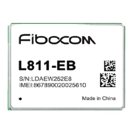
The product appearance for L811-EB module is shown in Figure 5-1: Figure 5-1 Module Appearance 5.2 Dimension of Structure The structural dimension of the L811-EB module is shown in Figure 5-2: Figure 5-2 Dimension of Structure(Unit:mm) Reproduction forbidden without Fibocom Wireless Inc. written authorization - All Rights Reserved. -
Page 44: Recommended Design For Pcb Bonding Pad
For the design of SMT stencil, solder paste, and the furnace temperature control, please refer to the SMT Application Design Specification. Reproduction forbidden without Fibocom Wireless Inc. written authorization - All Rights Reserved. L811-EB Hardware User Manual Page 44 of 47... -
Page 45: Storage
Oven: Heat convection oven. 5.6 Packing The L811-EB module uses the tray sealed vacuum packing, combined with the outer packing method using the hard cartoon box, so that the storage, transportation and the usage of modules can be protected to the greatest extent. -
Page 46: Tray Package
5.6.1 Tray Package The L811-EB module uses tray package, 20pcs are packed in each tray, with 5 trays in each box and 6 boxes in each case. Tray packaging process is shown in Figure 5-4: Figure 5-4 Tray Packaging Process Reproduction forbidden without Fibocom Wireless Inc. -
Page 47: Tray Size
175.0±0.5 6.5±0.3 0.5±0.1 35.4±0.3 28.0±0.3 ITEM 255.0±0.5 170.0±0.5 235.0±0.3 148.0±0.3 13.0±0.5 12.0±0.5 ITEM 13.0±0.5 148.0±0.2 80.0±0.2 8.5±0.2 Figure5-5 tray size Reproduction forbidden without Fibocom Wireless Inc. written authorization - All Rights Reserved. L811-EB Hardware User Manual Page 47 of 47...
Need help?
Do you have a question about the L811-EB and is the answer not in the manual?
Questions and answers