Table of Contents
Advertisement
Quick Links
Advertisement
Table of Contents

Subscribe to Our Youtube Channel
Related Manuals for Fibocom L811-EA Series


Summary of Contents for Fibocom L811-EA Series
- Page 1 L811-EA Series Module Hardware User Manual Version:V1.0.2 Date:2015.09.08...
- Page 2 Unless otherwise specified, the document only serves as the user guide. All the statements, information and suggestions contained in the document do not constitute any explicit or implicit guarantee. Trademark The trademark is registered and owned by Fibocom Wireless Inc. Versions Version Date Remarks V1.0.0...
- Page 3 Applicable Model List Type Note L811-EA The supported frequency bands of L811-EA wireless modules as shown in the following tables: Model No. LTE FDD WCDMA GSM/GPRS/EDGE Band L811-EA 1,2,3,4,5,7,8,13,17, Band 1,2,4,5,8 850/900/1800/1900 MHz 18,19,20 L811-EA Module Hardware User Manual Page 3 of 43...
-
Page 4: Table Of Contents
Content 1 Foreword..................................6 1.1 Introduction..............................6 1.2 Reference Standard............................6 2 Product Overview..............................8 2.1 Description..............................8 2.2 Specifications..............................8 2.3 Appearance..............................13 3 Structure...................................14 3.1 Dimension Diagram of Structure......................14 3.2 Recommended PCB Layout Design......................15 4 Hardware Introduction............................17 4.1 Pin Definition..............................17 4.1.1 Pin Map............................. - Page 5 5.4.2 W_DISABLE# Signal........................31 5.4.3 Android & Linux / Win8 & Win10 Dual Systems Switch Control Signal......... 31 5.5 USB Interface...............................32 5.5.1 USB Interface Definition......................... 32 5.5.2 USB Interface Application......................33 5.6 UART Interface............................33 5.6.1 UART Interface Description......................33 5.6.2 UART Interface Application......................34 5.7 USIM Interface.............................34 5.7.1 USIM Pins............................
-
Page 6: Foreword
1 Foreword 1.1 Introduction The document describes the electrical characteristics, RF performance, dimensions and application environment, etc. of L811-EA wireless modules. With the assistance of the document and other instructions, developers can quickly understand the performance of L811-EA wireless modules and develop products. - Page 7 3GPP TS 23.090 -v6.1.0: Unstructured Supplementary Service Data (USSD); Stage 2 3GPP TS 24.008 v6.19, Mobile radio interface Layer 3 specification; 3GPP TS 25.101 V7.18.0: User Equipment (UE) radio transmission and reception (FDD) 3GPP TS 36.101V9.18.0: User Equipment (UE) radio transmission and reception ...
-
Page 8: Product Overview
2 Product Overview 2.1 Description The L811-EA modules are highly integrated wireless communication LTE modules, which support three modes and twelve bands, including the 4G/3G/2G mainstream modes (LTE FDD/WCDMA/GSM) for Europe and North America and cover a wide range of frequency bands. The modules support the cellular communication networks of Europe, North America as well as the mobile operators in some regions of Asia. - Page 9 Performance Operating Voltage Voltage: 3.3V ~ 4.4V Normal: 3.8V 4mA (Sleep Mode) Current LTE FDD DATA:700mA Consumption WCDMA Talk:570mA (Typical Value) 2G Talk:250mA (GSM PCL5) Interfaces Antenna:Main x1,Diversity x1 RF Interface USB 2.0 x1,Multiple Profiles over USB SIM Support,I2C Support,I2S/PCM Support Function Interface GPIO,Clock Data Features...
- Page 10 FIBOCOM proprietary AT commands AT Commands GSM 07.05 GSM 07.07 Firmware Loader Tool over USB/UART Accessories User Manual Developer Kit Note: 1. Please make sure the temperature for device will not be higher than 85˚C. 2. The minimum distance between the user and/or any bystander and the radiating structure of the transmitter is 20cm.
- Page 11 Note: Federal Communications Commission (FCC) Declaration of Conformity This device complies with part 15 of the FCC Rules. Operation is subject to the following two conditions: (1) This device may not cause harmful interference, and (2) this device must accept any interference received, including interference that may cause undesired operation.
- Page 12 compliance requirement of the end product, which integrates this module. 20cm minimum distance has to be able to be maintained between the antenna and the users for the host this module is integrated into. Under such configuration, the FCC radiation exposure limits set forth for an population/uncontrolled environment can be satisfied.
-
Page 13: Appearance
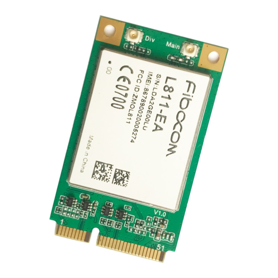
2.3 Appearance Top View: L811-EA Figure 2- 1 Top View Bottom view: Figure 2- 2 Bottom View L811-EA Module Hardware User Manual Page 13 of 43... -
Page 14: Structure
3 Structure 3.1 Dimension Diagram of Structure Figure 3- 1 Dimension Diagram of Structure L811-EA Module Hardware User Manual Page 14 of 43... -
Page 15: Recommended Pcb Layout Design
3.2 Recommended PCB Layout Design Figure 3- 2 Perspective drawing of top view L811-EA Module Hardware User Manual Page 15 of 43... - Page 16 Figure 3- 3 Structure Diagram of PCB Layout L811-EA Module Hardware User Manual Page 16 of 43...
-
Page 17: Hardware Introduction
4 Hardware Introduction 4.1 Pin Definition 4.1.1 Pin Map ANT_DI ANT_MA FSYS2_ RFE_RF VBAT VBAT FE1_VIO RFE_RF IPC_HO CORE_D FE1_SC ST_WA VBAT VBAT KEUP RFE_RF IPC_TRI FE1_SD TRST_N VRTC G_OUT HW_MO VSD2_1 TRIG_IN (TRC_D ATA0) HW_MO WAKEU IPC_TRI RESET_ P_HOST G_IN (TRC_C IPC_SL... -
Page 18: Description Of Pins
4.1.2 Description of Pins The logic signal level of L811-EA module is 1.8V. Reset Idle Pin# Pin Name Description Value Value Power VBAT Power input VBAT Power input VBAT Power input VBAT Power input VRTC VRTC output VSD2_1V8 VSD2_1V8 output POWER_ON/OFF#,RESET RESET_N Module reset input, pull up(100K ohms),1.8V... - Page 19 SIM1_DATA SIM1 data, internal 4.7K resistor pull up SIM1_CD SIM1 detect, pull up(390K ohms)CMOS 1.8V SIM1_DP USB data plus for SIM1 card SIM1_DN USB data minus for SIM1 card USB2.0 VBUS USB VBUS Supply USB_DN USB Data Minus USB_DP USB Data Plus USB3.0 HSIC High speed Inter IC clock (not supported...
- Page 20 UART1_CTS UART1 Clear To Send, CMOS 1.8V EINT WAKEUP WAKEUP,CMOS 1.8V W_DISABLE# W_DISABLE#,CMOS 1.8V EINT3 EINT3,CMOS 1.8V BODY_SAR BODY_SAR,CMOS 1.8V System status indicator CORE_DUMP Core dump indicator, CMOS 1.8V LPG,CMOS 1.8V WAKEUP_HOST WAKEUP_HOST,CMOS 1.8V PA_BLANKING/ PA blanking output/Monitoring Signal Output, TRIG_OUT(T_OUT1) CMOS 1.8V JTAG...
- Page 21 RFE_RFFE1_VIO RFFE1 VIO for tunable ANT,1.8V ANT_MAIN Main antenna ANT_DIV Diversity antenna L811-EA Module Hardware User Manual Page 21 of 43...
- Page 22 L811-EA Module Hardware User Manual Page 22 of 43...
- Page 23 TG10 TG11 TG12 TG13 TG14 TG15 TG16 H:High Voltage Level L:Low Voltage Level PD:Pull-Down PU:Pull-Up T:Tristate OD:Open Drain PP:Push-Pull Note : The unused pins can be left floating in case of circuit design. L811-EA Module Hardware User Manual Page 23 of 43...
-
Page 24: Hardware Interface
5 Hardware Interface 5.1 Power Interface 5.1.1 Power Supply The L811-EA module requires a 3.3V - 4.5V DC power supply that capable of supplying maximum GSM emission current which may up to 2A. Input power supply requirements: Parameter Minimum Value Recommended Value Maximum Value Unit... -
Page 25: Vrtc
Parameters Minimum Value Typical Value Maximum Value Unit VSD2_1V8 1.7135 1.8865 0.7* VSD2_1V8 1.8865 -0.3 0.3* VSD2_1V8 5.1.3 VRTC VRTC is the power supply for the internal RTC of the module. In order to let RTC work for a certain time when lost the VBAT power, as the backup power, it is recommended to add a big capacitor at the VRTC pin. -
Page 26: Power On/Off And Reset Signal
(1.8-1)*C/2 + (1-0.4)*C/1 = 0.4C + 0.6C = 1C When using a 100uF capacitor, the remaining time is 1*100 = 100 Sec. When using a 330uF capacitor, the remaining time is 1*330 = 330 Sec. If the RTC backup power function is not required, the VRTC pin can be left floating. 5.2 Power on/off and Reset Signal The L811-EA module provides two control signals for power on/off and reset functions. -
Page 27: Power Off
only needs to control the timing of RESET_N and POWER_ON/OFF# signals. 5.2.1.2 Power off The L811-EA module can be turned off by software or hardware control. Software control is preferred for normal cases, only when software control is not usable, then use the hardware control. By pulling down or ①... -
Page 28: The Recommended Design Of Power On/Off
5.2.1.3 The Recommended Design of Power on/off The recommended design of POWER_ON/ OFF# signal is as follows: L811-EA Figure 5- 4 Recommended Design of POWER_ON/OFF# Signal 5.2.2 RESET Signal The L811-EA module supports the external reset function. By controlling the RESET_N signal, the module will reset to its initial state. -
Page 29: Status Indicating Signals
Recommended design: L811-EA Figure 5- 5 Recommended Design of Reset Circuit 5.3 Status Indicating Signals Pin# Pin Name Description CORE_DUMP Core Dump Indicator LPG status Indicating WAKEUP_HOST The module wakes up the host (Application processor). PA_BLANKING PA Blanking output, external GPS control signal. 5.3.1 CORE DUMP Indicating The CORE_DUMP signal is used to indicate the mode of the module. -
Page 30: Wakeup_Host Signal
Idle (unregistered) 600ms high level and 600ms low level Idle (registered) 75ms high level and 3s low level Voice communication (Call) Always low level Data communication 75ms high level and 75ms low level Sleep (sleep mode) Always high level 5.3.3 WAKEUP_HOST Signal The WAKEUP_HOST signal is used to wake up the host when there are incoming calls, SMS or other data requests. -
Page 31: Interrupt Control Signal
5.4 Interrupt Control Signal The interrupt control signals as shown in the following tables: Pin# Name Description Wake up the module. WAKEUP Enable/Disable RF network. W_DISABLE# Android & Linux/Win8 & Win10 dual EINT3 systems switch. Body SAR detection. BODY_SAR 5.4.1 WAKE_UP Signal WAKE_UP signal description as shown in the following tables: Module Mode WAKE_UP Signal... -
Page 32: Usb Interface
For Android or Linux system, the module`s USB ports mapped as 3*ACM High/Floating ports. For Win8 or Win10 system, the module`s USB port is mapped as a MBIM mode. Description: 1. During booting, the implementation of Android & Linux / Win8 & Win10 system change is done by detecting the level of EINT3 signal. -
Page 33: Usb Interface Application
5.5.2 USB Interface Application Reference Circuit Design: L811-EA Figure 5- 6 USB Interface Reference Circuit Design The choice of capacitance for RV101 and RV102 TVS diodes should not greater than 1pF, it is recommended to use 0.5pF TVS diodes. There is no recommended capacitance value for RV100. VUSB pin supplies the power for USB, the recommended power range is 3.3V ~ 4.5V. -
Page 34: Uart Interface Application
The definition of UART1 signals as shown in the following tables: Pin# Pin Name Description UART1_CTS Clear to send UART1_RTS Request to send UART1_TXD Data Transmit UART1_RXD Date Receive 5.6.2 UART Interface Application The signal direction when connecting the UART1 of L811-EA module (DCE) and MCU (DTE) as shown in the following tables: MCU (DTE) application Signal direction... -
Page 35: Usim Interface Design
5.7.2 USIM Interface Design 5.7.2.1 “Normally Closed” SIM Card Circuit Design Reference Circuit Design:: Figure 5- 7 Reference Design of “Normally Closed” SIM Card Interface Normally closed SIM Connector: 1)When detaching the SIM card, pin 7 and pin 8 shorted together. 2)When inserting the SIM card, pin 7 and pin 8 opened. -
Page 36: Highlights For Usim Design
Note: In order to improve the EMC performance, the SIM card slot should be close to the module as much as possible. The filter capacitors for the SIM card signals should be placed close to the SIM card slot as much as possible. -
Page 37: Software Setup
(SW2), and Pin7 (SW1) is pulled up with a 4.7K resistor. When the SIM card is not inserted, SW2 and SW1 are opened, and SW2 is low. When the SIM card is inserted, SW2 and SW1 are shorted, and SIM1_CD signal will be pulled high. 5.7.4.2 Software Setup “+MSMPD”... -
Page 38: Pcm Mode Description
I2S2_CLK0 I2S_CLK I2S2_WA0 I2S_LRCK I2S2_RX I2S_SDOUT I2S2_TX I2S_SDIN Description: I2S interface can be configured as master or slave mode. It supports various audio sampling rates (48KHz, 44.1KHz, 32KHz, 24KHz, 22.5KHz, 16KHz, 12KHz, 11.025KHz and 8KHz). 5.8.2 PCM Mode Description L811-EA Signal Direction Audio CODEC PCM Port... -
Page 39: Clock Interface
Pin# Name Description I2C_DATA I2C data signal,1.8V signal level I2C_SCL I2C clock signal, 1.8V signal level The signal connection of L811-EA I2C master and external I2C slave ( such as an audio codec)as shown in the following tables: L811-EA Signal Direction Audio Codec I2C Port I2C_SDA I2C_SDA... -
Page 40: Electrical And Environmental Characteristic
6 Electrical and Environmental Characteristic 6.1 Electrical Characteristic The table below lists the range of L811-EA’s electrical characteristics: Parameters Minimum Value Maximum Value Unit Power supply signal Digital signal 6.2 Environmental Characteristic This table below shows the environmental features of L811-EA. Parameters Minimum Value Maximum Value... -
Page 41: Rf Interface
7 RF Interface 7.1 RF PCB Design 7.1.1 Wire Routing Principle The L811-EA module supports double RF antennas, the MAIN_ANT is for transmitting and receiving, and the DIV_ANT is for receiving. Diversity antenna can improve the receiver sensitivity as well as the downlink speed. -
Page 42: Impedance
7.1.2 Impedance The impedance of the RF signal line needs to be controlled at 50 Ohm. 7.2 Antenna Design 7.2.1 Main Antenna Design Requirements (1) Antenna efficiency Antenna efficiency is the ratio of the input power and radiant power. Because of the return loss, material loss and coupling loss of the antenna, the radiant power is always lower than the input power. - Page 43 antenna, and add appropriate filtering and shielding protection, or adding filtering devices on the traces. (7) TRP/TIS TRP (Total Radiated Power): GSM850/900>28dBm GSM DCS1800/PCS1900 >25dBm WCDMA Band 1,2,4,5,8>19dBm LTE FDD Band 1,2,3,4,5,7,8,13,17,18,19,20>19dBm TIS (Total Isotropic Sensitivity): ...
Need help?
Do you have a question about the L811-EA Series and is the answer not in the manual?
Questions and answers