Table of Contents
Advertisement
Quick Links
Advertisement
Table of Contents

Subscribe to Our Youtube Channel
Related Manuals for Fibocom LC116-LA


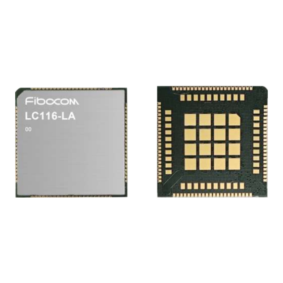
Summary of Contents for Fibocom LC116-LA
- Page 1 LC116-LA Hardware Guide V1.1...
- Page 2 All the statements, information and suggestions contained in the document do not constitute any explicit or implicit guarantee. Trademark The trademark is registered and owned by Fibocom Wireless Inc. Contact Company website: https://www.fibocom.com/ Address of headquarters: Floor 10-14, Block A, Building 6, Shenzhen International...
-
Page 3: Table Of Contents
3.3.3 Baseband Interface ..................... 24 3.3.4 RF Interface ......................25 3.3.5 Other interfaces ....................25 4 Circuit Design ....................34 4.1 Power Interface ......................34 4.1.1 Power input......................34 4.2 Control Interface ......................36 4.2.1 Pulse startup ......................36 Copyright © Fibocom Wireless Inc. - Page 4 4.4.7.1 PCM Interface Description ................52 4.4.7.2 PCM Signal Description ................52 4.4.8 Status Indicator ....................54 4.4.8.1 Network Status Indicator ................54 4.4.8.2 STATES ......................56 4.4.9 HSIC Interface* ..................... 56 4.4.10 LCD Interface ...................... 56 Copyright © Fibocom Wireless Inc.
- Page 5 5.1 Packaging ........................63 5.2 Storage .......................... 63 6 Appendix ....................... 64 6.1 GPRS and EGPRS Encoding Scheme ..............64 6.2 Acronyms and Abbreviations ................... 66 6.3 Related Documents ....................68 6.4 Reference Standards ....................68 Copyright © Fibocom Wireless Inc.
-
Page 6: Applicability Type
Applicability Type Applicability Type Applicability Type Description MCP is 2Gbit Flash+2Gbit RAM, and supports MAIN_ANT LC116-LA and DIV_ANT. Copyright © Fibocom Wireless Inc. -
Page 7: Change History
Change History Change History V1.0 (2021-11-10) Initial version V1.1 (2021-12-16) Updated the known issues. Copyright © Fibocom Wireless Inc. -
Page 8: Overview
The LC116-LA module is a broadband wireless terminal product based on Qualcomm 9X07 platform, applicable to multiple network systems and bands such as TDD-LTE, FDD-LTE, WCDMA and GSM. The following table lists the sub-models of the LC116-LA product. Table 1. Sub-models of the LC116-LA product... -
Page 9: Characteristics
Table 3. Baseband characteristics Category Description USB × 1, support USB2.0 C × 1 Function interface UART × 2 GPIOs USIM × 1, support single card single standby mode Peripheral interface LCD × 1 SGMII × 1 Copyright © Fibocom Wireless Inc. -
Page 10: System Architecture
Main antenna × 1 Antenna interface Diversity antenna × 1 1.3 System architecture The LC116-LA product hardware consists of the following parts: Baseband part: PMIC, MCP, USB, (U)SIM, PCM, I C, UART, SGMII, SDIO, GPIOs, GSM/CDMA/EVDO/WCDMA/TD-SCDMA/LTE TDD/LTE FDD controller RF part: RF Transceiver, RF PA, RF filter Antenna ... - Page 11 The module is in light sleep state. It is connected to a network and Sleep can receive paging messages. In this mode, the module can switch to the standby mode or PSM mode. Flight The wireless communication of the module is turned off. Copyright © Fibocom Wireless Inc.
-
Page 12: Technical Indicators
2 Technical Indicators 2 Technical Indicators 2.1 Physical Indicators Table 6. LC116-LA package mode Indicator Description Weight 5.2 g Package LCC+LGA 143 Pin Appearance dimensions (30.0±0.15) mm × (30.0±0.15) mm × (2.4±0.2) mm Structural dimensions See the figure below. The following figure shows the structural dimensions. - Page 13 DCS 1800MHz 1710–1785 1805–1880 LTE FDD Band 4 IMT 2100 1710–1755 2110–2155 LTE FDD/WCDMA/GSM Band 5 CLR 850MHz 824–849 869–894 LTE FDD Band 7 IMT 2600 2500–2570 2620–2690 LTE FDD/WCDMA/GSM Band 8 E-GSM 900MHz 880–915 925–960 Copyright © Fibocom Wireless Inc.
- Page 14 Tx (MHz) Rx (MHz) LTE FDD Band 28 IMT 700 703–748 758-803 LTE TDD Band 40 IMT 2300MHz 2300–2400 2300–2400 LC116-LA-10-90/91 does not support LTE. Table 8. Tx power System Band Tx Power (dBm) Description GSM850 32.5±1.5 GSM900 32.5±1.5 DCS1800 29.5±1.5 PCS1900 29.5±1.5...
- Page 15 -98.5 Band 3 -98.5 Band 4 -98.5 LTE FDD Band 5 -99.5 Band 7 -97.5 -98.5 Band 8 -98.5 Band 28 -97.5 LTE TDD Band 40 -98.5 Table 10. Main antenna indicator requirements Indicator Requirements Copyright © Fibocom Wireless Inc.
-
Page 16: Gnss Performance
LTE Band 7 (2600): 190 MHz LTE Band 8 (900): 80 MHz LTE Band 28 (700): 100 MHz LTE band 40 (2300): 100 MHz 2.3 GNSS Performance Table 11. Power consumption of module Average Parameter Mode Conditions Current (mA) Copyright © Fibocom Wireless Inc. - Page 17 Paging cycle #64 frames (USB sleep) LTE FDD Paging cycle #64 frames (USB wakeup) LTE TDD Paging cycle #64 frames (USB sleep) LTE TDD Paging cycle #64 frames (USB wakeup) AT+CFUN=0,0 (USB sleep) Radio off AT+CFUN=0,0 (USB wakeup) Copyright © Fibocom Wireless Inc.
- Page 18 LTE FDD Data transfer Band 4 @+23dBm LTE-RMS LTE FDD LTE FDD Data transfer Band 5 @+23dBm LTE FDD LTE FDD Data transfer Band 7 @+23dBm LTE FDD LTE FDD Data transfer Band 8 @+23dBm Copyright © Fibocom Wireless Inc.
-
Page 19: Electrical Indicators
-0.3 digital I/O The I/O interface level of the LC116-LA module is 1.8 V. When using the I/O interface, ensure that the level is matched. The following table describes the logic level range. Table 13. Logical level range of the module... -
Page 20: Application Environment
3 minutes, and the temperature conversion is repeated for 24 times. High temperature and humidity Temperature at +85℃±3°C, humidity at 85% RH, test lasting for 24 hours in shutdown state Copyright © Fibocom Wireless Inc. -
Page 21: Esd Indicators
2.7 ESD Indicators The design of LC116-LA module needs to consider ESD protection. The module pins have limited anti-static ability, and the key input/output signal interfaces must be handled with ESD measures. Reasonable structural design and PCB layout design can ensure that the metal shield shell is completely grounded, so as to improve the anti-static capability of the equipment. - Page 22 ESD simulator. Test contact non-contact ±8 ±10 discharge with an ESD simulator. Test contact non-contact Other interfaces ±0.5 ±1 discharge with an ESD simulator. The data is tested based on the ADP-LC116-LA-00-90 development board. Copyright © Fibocom Wireless Inc.
-
Page 23: Pins
Specific meaning of the pin and processing method when it is not used 3.2 Pin Distribution The LC116-LA module adopts LCC+LGA packaging, with a total of 143 pins, including 87 LCC pins and 56 LGA pins. The following figure shows the pin distribution. - Page 24 Connect all GND pins to the ground network. Ground pins 128-143. It is prohibited to pull PIN50, PIN52, PIN83, PIN85, PIN86, PIN96, PIN97, PIN98, PIN100, PIN102, and PIN103 to the high level before the module is successfully powered on. Copyright © Fibocom Wireless Inc.
-
Page 25: Pin Details
3s to 8s, and then release it. The module is powered off. When the module is in power-off mode, pull up USB_BOOT and insert USB_BOOT/COEX_RXD 1.8 V the USB. The module enters the download mode. Copyright © Fibocom Wireless Inc. -
Page 26: Baseband Interface
GPIO_43 1.8 V level before module successfully powered on. GPIO_54 1.8 V General input/output interface GPIO_42 1.8 V General input/output interface GPIO_49 1.8 V General input/output interface Copyright © Fibocom Wireless Inc. -
Page 27: Rf Interface
Main antenna, 50Ω, characteristic MAIN_ANT impedance 3.3.5 Other interfaces Table 22. LPG interface Pin No. Pin Name Power domain Description STATUS 1.8 V Module state indicator NETLIGHT 1.8 V Module network operating status Copyright © Fibocom Wireless Inc. - Page 28 Power Pin No. Pin Name Description domain SDIO_DATA1 1.8 V WLAN SDIO bus DATA1 SDIO_DATA2 1.8 V WLAN SDIO bus DATA2 SDIO_CMD 1.8 V WLAN SDIO bus command SDIO_DATA0 1.8 V WLAN SDIO bus DATA0 Copyright © Fibocom Wireless Inc.
- Page 29 BT_PCM_SYNC DO 1.8 V level before module successfully powered on. USIM_DET/BT_EN 1.8 V SIM card detection/Bluetooth enable Table 27. HSIC interface* Power Pin No. Pin Name Description domain Copyright © Fibocom Wireless Inc.
- Page 30 WLAN enabling. It is prohibited to pull DO 1.8 V it up to the high level before the WLAN_EN module is successfully powered on. WOWWAN DO 1.8 V Wake up the host WL_PWR_EN DO 1.8 V WLAN power enabling Copyright © Fibocom Wireless Inc.
- Page 31 (U)SIM data signal line. It needs to be USIM_DATA 1.8 V/3 V pulled up to USIM_VDD externally. USIM_RST 1.8 V/3 V (U)SIM reset signal line USIM_CLK 1.8 V/3 V (U)SIM clock signal line USIM_VDD 1.8 V/3 V (U)SIM power supply, the module Copyright © Fibocom Wireless Inc.
- Page 32 SD card insertion detection. Active low SD_DET 1.8 V by default Table 33. UART interface Power Pin No. Pin Name Description domain 1.8 V Request to send 1.8 V Clear to send 1.8 V Ring prompt 1.8 V Carrier detection Copyright © Fibocom Wireless Inc.
- Page 33 SGMII_RX_M negative signal SGMII_RST_N 1.8/2.85 V Ethernet reset SGMII_INT_N 1.8 V Ethernet interrupt SGMII differential data sending SGMII_TX_M negative signal, close to PHY string 0.1 uF capacitor SGMII_TX_P SGMII differential data sending Copyright © Fibocom Wireless Inc.
- Page 34 LCD_D6 1.8 V LCD bus data bit 6 LCD_D7 1.8 V LCD bus data bit 7 PCM_OUT/LCD_D8 1.8 V PCM data output/LCD bus data bit 4 Sleep mode control/LCD bus reset DTR/LCD_NRST 1.8 V signal Copyright © Fibocom Wireless Inc.
- Page 35 LCD_WE_N 1.8 V enabling PCM synchronization signal/LCD bus PCM_SYNC/LCD_TE 1.8 V data synchronization PCM_CLK/LCD_NCS 1.8 V PCM clock signal/LCD bus chip select The "*" symbol in the document indicates that the item is under development. Copyright © Fibocom Wireless Inc.
-
Page 36: Circuit Design
DC power supply is not lower than the minimum voltage. The VBAT power supply of LC116-LA module requires star wiring to the power supply pins. The following figure shows the recommended design of the power supply. - Page 37 Filter out interference caused Filter capacitor 1 uF, 100 nF by clock and digital signals. Eliminate low-frequency and Decoupling 39 pF, 33 pF intermediate-frequency capacitor interference. Eliminate high-frequency RF Decoupling 18 pF, 6.8 pF, 8.2 pF interference. capacitor Copyright © Fibocom Wireless Inc.
-
Page 38: Control Interface
Figure 6. OC driver startup reference circuit Another way to control the PWRKEY pin is to use a button switch. A TVS (ESD9X5VL-2/TR recommended) should be placed near the button for ESD taken. The following figure Copyright © Fibocom Wireless Inc. -
Page 39: Auto Power-On
It is recommended to control the interval from power-up by VBAT to PWRKEY pin pull-down no less than 30ms. 4.2.2 Auto power-on To implement auto power-on, ground the PWRKEY pin. In this case, the module can be powered off by disconnecting the power supply. Copyright © Fibocom Wireless Inc. -
Page 40: Power-Off
When using the AT command to power off the module, ensure that the PWRKEY pin is always at the high level after the power-off command is executed. Otherwise, the module will automatically power on again. The following figure shows the power-off timing sequence. Copyright © Fibocom Wireless Inc. -
Page 41: Reset
Module reset method: Pull down the RESET_N pin for 700 ms to 1s, and then release or send the AT command AT+RESET. Clients can control the RESET_N pin by OC/OD driver circuit and button switch. The following figure shows the reference circuits. Figure 10. OC driver reset reference circuit Copyright © Fibocom Wireless Inc. - Page 42 RESET is a sensitive signal. During PCB layout, keep these signals far away from RF interference. PCB routes must be protected using GND and kept away from edges of PCBs to avoid module reset due to ESD problems. Copyright © Fibocom Wireless Inc.
-
Page 43: Operating Mode
4 Circuit Design 4.3 Operating Mode 4.3.1 Flight mode The following table describes the W_DISABLE# pin of the LC116-LA module. Table 39. Flight mode interface Power Pin No. Pin Name Description domain W_DISABLE#/BT_PCM_IN 1.8 V Flight mode control/PCM input signal LC116-LA module supports two ways to enter flight mode: Table 40. -
Page 44: Supported)
Unplug the USB cable or turn off the USB Hub master controller. The module will enter sleep mode. Wake mode: Insert the USB or turn on the USB master controller. The module will wake up. Copyright © Fibocom Wireless Inc. -
Page 45: Usb Application (Usb Suspend Supported)
The USB ports of the module cannot contain adb ports, for example, +GTUSBMODE=17. Power consumption of the module in idle state can be implement by the following commands and steps: 1. AT+DISK=0,0,0 2. AT+GTUSBDETECTEN=1 3. AT+SYSCMD=echo off > /sys/power/autosleep 4. Remove the USB cable. Copyright © Fibocom Wireless Inc. -
Page 46: Baseband Interface
The USB data cable cannot be routed under the crystal, oscillator, magnetic device, or RF signal. It is recommended to take an inner differential cable that is wrapped with copper connected to the ground at all directions. Copyright © Fibocom Wireless Inc. -
Page 47: Uart
The serial port level of the LC116-LA series module is 1.8 V. If the level of the host system is 3.3 V or another value, a level converter is needed between the module and the host. -
Page 48: I 2 C
C interfaces are all open-drain outputs. When using these interfaces, please pull up to 1.8 V power domain through external pull-up resistors. When I C has more than one peripheral, please ensure the uniqueness of every peripheral address. When mounting Copyright © Fibocom Wireless Inc. -
Page 49: Sd Card
40 mm. If the cabling length is equal to or less than 10 mm, the cabling length difference of the clock signal line and data signal line should be controlled equal to or less than 1 mm. Copyright © Fibocom Wireless Inc. -
Page 50: Adc
The module has a built-in (U)SIM card interface, and supports 1.8 V and 3.0 V (U)SIM card. 4.4.6.1 (U)SIM Card Connector with Card Detection Signal During (U)SIM design, you must select a (U)SIM card connector. A hot plugging card connector (recommended model: SIM016-8P-220P) with (U)SIM card detection function is recommended. Copyright © Fibocom Wireless Inc. - Page 51 When (U)SIM card is inserted, USIM_PRESENCE pin is at a high level. When (U)SIM card is removed, USIM_PRESENCE pin is at a low level. Figure 18. Reference circuit design of a (U)SIM card connector with card detection signals Copyright © Fibocom Wireless Inc.
-
Page 52: U)Sim Card Connector Without Card Detection Signals
RV1 to RV5 is EGA10402V05A2. 4.4.6.3 (U)SIM Hot Plugging The LC116-LA module supports (U)SIM card hot plugging function. The module determines whether the (U)SIM card is in place by detecting the state of the USIM_PRESENCE pin. The (U)SIM card hot plugging function is enabled by default. When... -
Page 53: U)Sim Card Design Requirements
SIM card signal line and the ground. USIM_DATA is pulled up to USIM_VDD via a 10 kΩ resistor. 4.4.7 PCM The LC116-LA module provides a digital audio interface PCM for communication with external codec and other digital audio devices. Copyright © Fibocom Wireless Inc. -
Page 54: Pcm Interface Description
The main chip of the module uses PCM signals that comply with the European E1 standard. PCM_CLK works at 2.048 MHz and uses 16-bit linear coding format. PCM_SYNC is a short pulse of 8 kHz (488 nS). Figure 20. PCM_SYNC timing sequence Copyright © Fibocom Wireless Inc. - Page 55 4 Circuit Design Figure 21. Timing sequence of PCM_CODEC to LC116-LA module Figure 22. Timing sequence of LC116-LA module to PCM_CODEC Table 42. Codec timing sequence parameters Time Parameter Unit t(sync) PCM_SYNC cycle time μs t(synca) PCM_SYNC asserted time t(syncd) PCM_SYNC deasserted time 124.5...
-
Page 56: Status Indicator
4.4.8 Status Indicator 4.4.8.1 Network Status Indicator The PIN51 of the LC116-LA module is the network status indicator signal interface. The network status indicator interface is used to drive the status indicator. The following table describes the working status of the module network indicator. - Page 57 75 ms at high level or 75 ms at low level Established a data connection Low level Voice call High level Sleep status The following figure shows the reference circuit of network status indicator. Figure 23. Reference circuit for the network status indicator Copyright © Fibocom Wireless Inc.
-
Page 58: States
4 Circuit Design 4.4.8.2 STATES PIN49 of the LC116-LA module is the module status indicator signal interface. The STATES indicator is used to indicate the working status of the module, and it outputs a high level after the module is powered on. The following figure shows the reference circuit of the STATES indicator. -
Page 59: Sgmii
The following figure shows the reference circuit of the LCD interface using H.028.015A01 LCD screen. Figure 25. LCD reference circuit 4.4.11 SGMII The LC116-LA module provides an SGMII interface with embedded Ethernet MAC. The characteristics are as follows: It complies with IEEE 802.3 standard. ... -
Page 60: Rf Part
4 Circuit Design Figure 26. Simple diagram of the Ethernet application scheme The following figure shows the reference design of the SGMII interface of the LC116-LA module connected to Ethernet PHY chip such as AR8033. Figure 27. Reference design of the SGMII interface 4.5 RF Part... - Page 61 At this time, there impedance is no power reflection at the terminal of the feeder, and there is no standing wave on the feeder. The input impedance of the antenna changes smoothly with frequency. Copyright © Fibocom Wireless Inc.
-
Page 62: Impedance Design
50Ω. Microstrip cable complete structure Figure 28. Two-layer PCB microstrip line structure Coplanar waveguide complete structure Copyright © Fibocom Wireless Inc. - Page 63 Figure 31. Four-layer PCB coplanar waveguide structure (see ground layer 4) In the design of RF antenna interface circuit, in order to ensure good performance and reliability of the RF signal, it is recommended to observe the following principles: Copyright © Fibocom Wireless Inc.
- Page 64 GND) between the module and antenna connector (or feeding point) for antenna debugging. Two parallel components are directly connected across the RF cable, and the branch must not be pulled out. Main Module antenna ANT_MAIN Diversity antenna ANT_DIV Figure 32. Antenna reference design Copyright © Fibocom Wireless Inc.
-
Page 65: Packaging And Storage
5 Packaging and Storage 5 Packaging and Storage 5.1 Packaging FIBOCOM LC116 Series SMT Design Guide For packaging and storage, please refer to 5.2 Storage Storage conditions (recommended): The temperature is 23±5℃; the relative humidity is 35%-70%. Storage period (sealed vacuum packaging): 12 months under the recommended storage conditions. -
Page 66: Appendix
Active timeslots indicate the total number of timeslots that the GPRS device can use for both uplink and downlink communication. Table 46. Multislot allocation of different classes Multislot Class Downlink Slots Uplink Slots Active Slots Copyright © Fibocom Wireless Inc. - Page 67 CS-3 GMSK 15.6kbps 31.2kbps 62.4kbps CS-4 GMSK 21.4kbps 42.8kbps 85.6kbps MCS-1 GMSK 8.80kbps 17.6kbps 35.2kbps MCS-2 GMSK 11.2kbps 22.4kbps 44.8kbps MCS-3 GMSK 14.8kbps 29.6kbps 59.2kbps MCS-4 GMSK 17.6kbps 35.2kbps 70.4kbps MCS-5 8-PSK 22.4kbps 44.8kbps 89.6kbps Copyright © Fibocom Wireless Inc.
-
Page 68: Acronyms And Abbreviations
GMSK Gaussian Minimum Shift Keying Global System for Mobile Communications Imax Maximum Load Current Long Term Evolution Carrier Aggregation Printed Circuit Board Phase Shift Keying Quadrature Amplitude Modulation QPSK Quadrature Phase Shift Keying Radio Frequency Copyright © Fibocom Wireless Inc. - Page 69 Maximum Output High Level Voltage Value VOHmin Minimum Output High Level Voltage Value VOLmax Maximum Output Low Level Voltage Value VOLmin Minimum Output Low Level Voltage Value VSWR Voltage Standing Wave Ratio WCDMA Wideband Code Division Multiple Access Copyright © Fibocom Wireless Inc.
-
Page 70: Related Documents
FIBOCOM LC116 AT Command Manual FIBOCOM FG101_Hardware Guide_EVB FIBOCOM LC116 LCC SMT Application Design Specification 6.4 Reference Standards This product is designed with reference to the following standards: 3GPP TS 51.010-1 V10.5.0: Mobile Station (MS) conformance specification; Part 1: ... - Page 71 3GPP TS 27.007 V10.0.8: AT command set for User Equipment (UE) 3GPP TS 27.005 V10.0.1: Use of Data Terminal Equipment - Data Circuit terminating Equipment (DTE - DCE) interface for Short Message Service (SMS) and Cell Broadcast Service (CBS) Copyright © Fibocom Wireless Inc.
- Page 72 Fibocom Wireless Inc. that they wish to change the antenna trace design. In this case, a Class II permissive change application is required to be filed Copyright ©...
- Page 73 FCC ID/IC ID cannot be used on the final product. In these circumstances, the OEM integrator will be responsible for re-evaluating the end product (including the transmitter) and obtaining a separate FCC/IC authorization. Copyright © Fibocom Wireless Inc.
- Page 74 - Increase the separation between the equipment and receiver. - Connect the equipment into an outlet on a circuit different from that to which the receiver is connected. - Consult the dealer or an experienced radio/TV technician for help. Copyright © Fibocom Wireless Inc.
- Page 75 2) The transmitter module may not be co-located with any other transmitter or antenna. As long as 2 conditions above are met, further transmitter test will not be required. However, the OEM integrator is still responsible for testing their end-product for any additional Copyright © Fibocom Wireless Inc.
- Page 76 Radiation Exposure Statement This equipment complies with FCC radiation exposure limits set forth for an uncontrolled environment. This equipment should be installed and operated with minimum distance 20 cm between the radiator & your body. Copyright © Fibocom Wireless Inc.
Need help?
Do you have a question about the LC116-LA and is the answer not in the manual?
Questions and answers