Table of Contents
Advertisement
Quick Links
Advertisement
Table of Contents

Related Manuals for Fibocom FG360-NA


Summary of Contents for Fibocom FG360-NA
- Page 1 FG360-NA Hardware Guide Version: Draft V1.0.2 Date: 2021-05-06...
- Page 2 Applicability Type Product Model Description Reproduction forbidden without Fibocom Wireless Inc. written authorization - All rights reserved. FG360-NA Hardware Guide 2/28...
- Page 3 Trademark The trademark is registered and owned by Fibocom Wireless Inc. Reproduction forbidden without Fibocom Wireless Inc. written authorization - All rights reserved. FG360-NA Hardware Guide 3/28...
- Page 4 Section 4.1: Update module appearance Section 3.1: Add PCIe D as reserved and update pin name of Pin 3,265,38,39,41,44 Peng Yujun V1.0.0 2021-03-09 Initial version Xu Xialin Reproduction forbidden without Fibocom Wireless Inc. written authorization - All rights reserved. FG360-NA Hardware Guide 4/28...
-
Page 5: Table Of Contents
Table of Pin No. and Pin Name ..................17 3.1.2 Pin Definition ......................... 19 Structural Specification ....................27 Product Appearance ....................27 Dimension of Structure ....................27 Storage ........................28 Packing........................28 Reproduction forbidden without Fibocom Wireless Inc. written authorization - All rights reserved. FG360-NA Hardware Guide 5/28... -
Page 6: Foreword
The document describes the electrical characteristics, RF performance, dimensions and application environment, etc. of FG360-NA (hereinafter referred to as FG360). With the assistance of the document and other instructions, the developers can quickly understand the hardware functions of FG360 modules and develop products. - Page 7 One set of I2C interface, data transmission rate up to 400Kbit/s ADCs , Voltage Range: 0~1.45V A/D conversion channel Software Firmware update USB/PCIe/FOTA Operating System Linux/Android/Windows Reproduction forbidden without Fibocom Wireless Inc. written authorization - All rights reserved. FG360-NA Hardware Guide 7/28...
- Page 8 1. When temperature keeps in the range of -30~75°C, the module can work normally. Module performance meets the 3GPP specifications. 2. When temperature keeps in the range of -40~85°C, module performance may be slightly out of 3GPP specifications. Reproduction forbidden without Fibocom Wireless Inc. written authorization - All rights reserved. FG360-NA Hardware Guide 8/28...
-
Page 9: Application Framework
Sleep CLK 32KHz Baseband Sub PMU eSIM Coex USIM1 SGMII PCIe3.0 USB2.0/3.0 UART ADCs MIPI JTAG GPIO/EINT SDIO UART Figure 2-1 Hardware block diagram Reproduction forbidden without Fibocom Wireless Inc. written authorization - All rights reserved. FG360-NA Hardware Guide 9/28... -
Page 10: Antenna Configuration
Part 15 Subpart B or emissions are complaint with the transmitter(s) rule(s). The Grantee will provide guidance to the host manufacturer for Part 15 B requirements if needed. Reproduction forbidden without Fibocom Wireless Inc. written authorization - All rights reserved. FG360-NA Hardware Guide... - Page 11 Important Note notice that any deviation(s) from the defined parameters of the antenna trace, as described by the instructions, require that the host product manufacturer must notify to Fibocom Wireless Inc. that they wish to change the antenna trace design. In this case, a Class II permissive change application is required to be filed by the USI, or the host manufacturer can take responsibility through the change in FCC ID (new application) procedure followed by a Class II permissive change application.
- Page 12 This equipment complies with FCC radiation exposure limits set forth for an uncontrolled environment. This equipment should be installed and operated with minimum distance 20 cm between the radiator & your body. Reproduction forbidden without Fibocom Wireless Inc. written authorization - All rights reserved. FG360-NA Hardware Guide 12/28...
- Page 13 Cet appareil est conçu uniquement pour les intégrateurs OEM dans les conditions suivantes: (Pour utilisation de dispositif module) Reproduction forbidden without Fibocom Wireless Inc. written authorization - All rights reserved. FG360-NA Hardware Guide 13/28...
- Page 14 Manual Information To the End User The OEM integrator has to be aware not to provide information to the end user regarding how to Reproduction forbidden without Fibocom Wireless Inc. written authorization - All rights reserved. FG360-NA Hardware Guide 14/28...
- Page 15 RF dans le manuel de l'utilisateur du produit final qui intègre ce module. Le manuel de l'utilisateur final doit inclure toutes les informations réglementaires requises et avertissements comme indiqué dans ce manuel. Reproduction forbidden without Fibocom Wireless Inc. written authorization - All rights reserved. FG360-NA Hardware Guide 15/28...
-
Page 16: Pin Definition
CLOCK Pins Figure 3-1 Pin map Note: The pin "RESERVED" means that the position pin is reserved and does not need to be connected. Reproduction forbidden without Fibocom Wireless Inc. written authorization - All rights reserved. FG360-NA Hardware Guide 16/28... -
Page 17: Table Of Pin No. And Pin Name
127~128 DBG_UART_TX ANT8_M 131~134 BT_UTXD 136~137 BT_URXD ANT7_D DSI_TE 142~143 EINT16 145~147 ANT6 BT_PRI_RXD 151~152 BT_ACT_TXD 154~155 DISP_PWM ANT5_M2 GPIO78/ USB_DRVBUS 160~161 163~164 PCIE_D_CLKREQN Reproduction forbidden without Fibocom Wireless Inc. written authorization - All rights reserved. FG360-NA Hardware Guide 17/28... - Page 18 PCIE_C_LN0_RXN PCIE_C_LN0_RXP PCIE_C_LN0_TXP PCIE_C_LN0_TXN 397~398 PCIE_C_CLKP PCIE_C_CLKN PCIE_C_PERSTN PCIE_C_CLKREQN 403 PCIE_C_PEWAKEN 404 DSI0_D0P DSI0_D0N DSI0_CKN DSI0_CKP DSI0_D1N DSI0_D1P 410~425 RESERVED RESERVED RESERVED RESERVED RESERVED Reproduction forbidden without Fibocom Wireless Inc. written authorization - All rights reserved. FG360-NA Hardware Guide 18/28...
-
Page 19: Pin Definition
USB high speed data minus USB_DP USB high speed data plus VBUS_DET USB VBUS detection USB_DRVBUS VDD_EXT_1V8 PD USB OTG power enable USB_ID VDD_EXT_1V8 PD USB ID USIM Reproduction forbidden without Fibocom Wireless Inc. written authorization - All rights reserved. FG360-NA Hardware Guide 19/28... - Page 20 External Tuner MIPI Control MIPI1_D_SDATA VDD_EXT_1V8 PD Data Pin External Tuner MIPI Control MIPI1_D_SCLK VDD_EXT_1V8 PD Clock Pin External Tuner MIPI Control MIPI2_D_SDATA VDD_EXT_1V8 PD Data Pin Reproduction forbidden without Fibocom Wireless Inc. written authorization - All rights reserved. FG360-NA Hardware Guide 20/28...
- Page 21 SGMII 0 receive data minus AVDD12_SGMI SGMII_0_RXP SGMII 0 receive data plus AVDD12_SGMI SGMII_0_TXN SGMII 0 transmit data minus AVDD12_SGMI SGMII_0_TXP SGMII 0 transmit data plus Reproduction forbidden without Fibocom Wireless Inc. written authorization - All rights reserved. FG360-NA Hardware Guide 21/28...
- Page 22 2+2+4 and 4+4+4 WIFI/BT VDD_EXT_1V8 PD PCIE_D_PERSTN and RF co-exist control signals GPIO77/ MT6890 GPIO, used for VDD_EXT_1V8 PD PCIE_D_PEWAKEN 2+2+4 and 4+4+4 WIFI/BT Reproduction forbidden without Fibocom Wireless Inc. written authorization - All rights reserved. FG360-NA Hardware Guide 22/28...
- Page 23 SPI0_CLK VDD_EXT_1V8 PD SPI interface clock signal AUDIO CODEC CDC_RESET_N VDD_EXT_1V8 PD External CODEC reset signal External CODEC interrupt CDC_INT1_N VDD_EXT_1V8 PD signal Reproduction forbidden without Fibocom Wireless Inc. written authorization - All rights reserved. FG360-NA Hardware Guide 23/28...
- Page 24 DSI LCD MIPI lane1 minus DSI0_D1P AVDD12_DSI DSI LCD MIPI lane1 plus WIFI/BT BT_UTXD VDD_EXT_1V8 PD UART TX signal BT_URXD VDD_EXT_1V8 PD UART RX signal Reproduction forbidden without Fibocom Wireless Inc. written authorization - All rights reserved. FG360-NA Hardware Guide 24/28...
- Page 25 WIFI control signal 2, WIFI_GPIO2 VDD_EXT_1V8 PD Reserved Reserved Reserved Reserved Reserved Reserved Reserved Reserved Reserved Reserved Reserved Reserved Reserved Reserved 23, 32, 48, RESERVED 293,426~430 Reproduction forbidden without Fibocom Wireless Inc. written authorization - All rights reserved. FG360-NA Hardware Guide 25/28...
- Page 26 1. The PWRKEY and SYS_RESIN_N pins have internal pull-up, and the pull-up power supply is in exclusive mode; no external pull-up is required; PON_1 pin module with weak pull-down, maximum input voltage must not exceed VBAT_BB. Reproduction forbidden without Fibocom Wireless Inc. written authorization - All rights reserved. FG360-NA Hardware Guide 26/28...
-
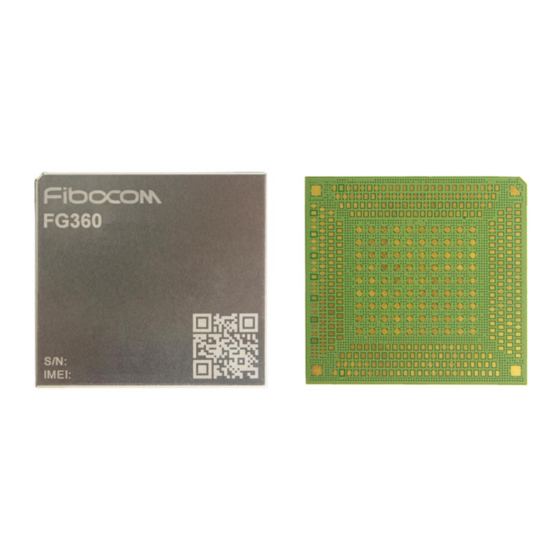
Page 27: Structural Specification
4.2 Dimension of Structure The structural dimensions of the FG360 module are shown in the figure: Figure 4-2 Structure size chart Note: Unmarked dimensional tolerances are 0.1mm. Reproduction forbidden without Fibocom Wireless Inc. written authorization - All rights reserved. FG360-NA Hardware Guide 27/28... -
Page 28: Storage
4.3 Storage Refer to FIBOCOM FG360-NA Series SMT Design Guide. 4.4 Packing Refer to FIBOCOM FG360-NA Series SMT Design Guide. Reproduction forbidden without Fibocom Wireless Inc. written authorization - All rights reserved. FG360-NA Hardware Guide 28/28...
Need help?
Do you have a question about the FG360-NA and is the answer not in the manual?
Questions and answers