Fibocom L860-GL Hardware User Manual
Hide thumbs
Also See for L860-GL:
- Hardware user manual (54 pages) ,
- At command user manual (254 pages)
Table of Contents
Advertisement
Advertisement
Table of Contents

Subscribe to Our Youtube Channel
Related Manuals for Fibocom L860-GL


Summary of Contents for Fibocom L860-GL
- Page 1 FIBOCOM_L860-GL Hardware User Manual Version:1.0.2 Date:2018-07-28...
- Page 2 All the statements, information and suggestions contained in the document do not constitute any explicit or implicit guarantee. Reproduction forbidden without Fibocom Wireless Inc. written authorization - All Rights Reserved. FIBOCOM_L860-GL Hardware User Manual...
-
Page 3: Lte Band
Host manufacturer is responsible for ensuring that the host continues to be compliant with the Part 15 subpart B unintentional radiator requirements after the module is installed and operational. Reproduction forbidden without Fibocom Wireless Inc. written authorization - All Rights Reserved. FIBOCOM_L860-GL Hardware User Manual... - Page 4 RF module in the user’s manual of the end product which integrates this module. The end user manual shall include all required regulatory information/warning as show in this manual. Reproduction forbidden without Fibocom Wireless Inc. written authorization - All Rights Reserved. FIBOCOM_L860-GL Hardware User Manual...
- Page 5 The antenna must be installed such that 20 cm is maintained between the antenna and users, and the Max allowed antenna gain is as following table showed Reproduction forbidden without Fibocom Wireless Inc. written authorization - All Rights Reserved. FIBOCOM_L860-GL Hardware User Manual...
- Page 6 LTE BAND 26 8.25 (824-849) LTE BAND 30 1.00 LTE BAND 38 9.00 LTE BAND 41 5.50 LTE BAND 66 6.00 Reproduction forbidden without Fibocom Wireless Inc. written authorization - All Rights Reserved. FIBOCOM_L860-GL Hardware User Manual Page 6 of 55...
- Page 7 1. Modify B41 HPUE maximum TX power description V1.0.3 2018-07-28 2. Delete Band21/Band32 Related Information Applicability Table Product model Description L860-GL-01 Reproduction forbidden without Fibocom Wireless Inc. written authorization - All Rights Reserved. FIBOCOM_L860-GL Hardware User Manual Page 7 of 55...
-
Page 8: Table Of Contents
3.4.1.2 PCIe Interface Application ..................32 3.4.2 USB Interface ........................34 3.4.2.1 USB Interface Definition ................... 34 3.4.2.2 USB2.0 Interface Application ................... 34 Reproduction forbidden without Fibocom Wireless Inc. written authorization - All Rights Reserved. FIBOCOM_L860-GL Hardware User Manual Page 8 of 55... - Page 9 5.1 Dimension of Structure ......................... 51 5.2 M.2 Interface Model ........................51 5.3 M.2 Connector ..........................52 5.4 Storage ............................53 Reproduction forbidden without Fibocom Wireless Inc. written authorization - All Rights Reserved. FIBOCOM_L860-GL Hardware User Manual Page 9 of 55...
- Page 10 5.4.1 Storage Life ........................53 5.5 Packing ............................53 5.5.1 Tray Package ........................53 5.5.2 Tray size ..........................55 Reproduction forbidden without Fibocom Wireless Inc. written authorization - All Rights Reserved. FIBOCOM_L860-GL Hardware User Manual Page 10 of 55...
-
Page 11: Foreword
The document describes the electrical characteristics, RF performance, dimensions and application environment, etc. of L860-GL (hereinafter referred to as L860). With the assistance of the document and other instructions, the developers can quickly understand the hardware functions of L860 modules and develop products. -
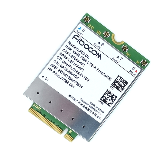
Page 12: Overview
Weight: About 6.2 g Interface WWAN Antenna x 4 Antenna Connector Support 4x4 MIMO Dual SIM, 3V/1.8V Function Interface PCIe 2.0 X1 Reproduction forbidden without Fibocom Wireless Inc. written authorization - All Rights Reserved. FIBOCOM_L860-GL Hardware User Manual Page 12 of 55... -
Page 13: Ca Combinations
5+7, 30, 46, 66 7+8, 20, 28, 32, 46 12+30, 66 Inter-band 13+46, 66 14+30, 66 25+26, 41, 46 26+41 29+30, 66 30+66 Reproduction forbidden without Fibocom Wireless Inc. written authorization - All Rights Reserved. FIBOCOM_L860-GL Hardware User Manual Page 13 of 55... - Page 14 2 intra-band(contiguous) plus 2 1+3+3+7+7, 3+3+7+7+28*, 2+46+46+46+46*, intra-band(contiguous) plus inter- 46+46+46+46+66* band 2 intra-band(contiguous) plus 3 1+3+3+7+20*, 1+3+7+7+28*, 2+5+5+30+66* inter-band Reproduction forbidden without Fibocom Wireless Inc. written authorization - All Rights Reserved. FIBOCOM_L860-GL Hardware User Manual Page 14 of 55...
-
Page 15: Application Framework
The hardware block diagram in Figure 2-2 shows the main hardware functions of L860 module, including base band and RF functions. Reproduction forbidden without Fibocom Wireless Inc. written authorization - All Rights Reserved. FIBOCOM_L860-GL Hardware User Manual Page 15 of 55... -
Page 16: Antenna Configuration
4x4 MIMO supported bands receive MIMO2 ANT 4x4 MIMO supported bands receive Diversity & GNSS ANT All supported bands and GNSS receive Reproduction forbidden without Fibocom Wireless Inc. written authorization - All Rights Reserved. FIBOCOM_L860-GL Hardware User Manual Page 16 of 55... -
Page 17: Application Interface
The L860 module applies standard M.2 Key-B interface, with a total of 75 pins. 3.1.1 Pin Map Figure 3-1 Pin Map Note: Pin “Notch” represents the gap of the gold fingers. Reproduction forbidden without Fibocom Wireless Inc. written authorization - All Rights Reserved. FIBOCOM_L860-GL Hardware User Manual Page 17 of 55... -
Page 18: Pin Definition
NC, L860 M.2 module is configured as the WWAN – PCIe, USB3.0 interface CONFIG_0 type I2S Serial receive data, I2S_RX CMOS 1.8V Reserved Reproduction forbidden without Fibocom Wireless Inc. written authorization - All Rights Reserved. FIBOCOM_L860-GL Hardware User Manual Page 18 of 55... - Page 19 1.8V/3V Power Supply UIM2_RESET SIM2 reset signal 1.8V/3V PCIe RX Differential signals PERn0 Negative UIM2_PWR SIM2 power supply, 3V/1.8V 1.8V/3V Reproduction forbidden without Fibocom Wireless Inc. written authorization - All Rights Reserved. FIBOCOM_L860-GL Hardware User Manual Page 19 of 55...
- Page 20 Wireless Coexistence between WWAN and WiFi/BT modules, based on BT-SIG COEX3 CMOS 1.8V coexistence protocol. COEX_EXT_FTA, Reserved ANTCTL1 Tunable ANT CTRL1 CMOS 1.8V Reproduction forbidden without Fibocom Wireless Inc. written authorization - All Rights Reserved. FIBOCOM_L860-GL Hardware User Manual Page 20 of 55...
- Page 21 Reset Value: The initial status after module reset, not the status when working. H: High Voltage Level Low Voltage Level PD: Pull-Down PU: Pull-Up Tristate Reproduction forbidden without Fibocom Wireless Inc. written authorization - All Rights Reserved. FIBOCOM_L860-GL Hardware User Manual Page 21 of 55...
-
Page 22: Power Supply
The L860 module should be powered through the +3.3V pins, and the power supply design is shown in Figure 3-2: Reproduction forbidden without Fibocom Wireless Inc. written authorization - All Rights Reserved. FIBOCOM_L860-GL Hardware User Manual Page 22 of 55... - Page 23 The power supply requirement is shown in Figure 3-3: Burst transmit Burst transmit Ripple≤300mV Power supply Drop VBAT≥3.135V min:3.135V Figure 3-3 Power Supply Requirement Reproduction forbidden without Fibocom Wireless Inc. written authorization - All Rights Reserved. FIBOCOM_L860-GL Hardware User Manual Page 23 of 55...
-
Page 24: Logic Level
WCDMA Data call Band 4 @+23.5dBm WCDMA WCDMA-RMS WCDMA Data call Band 5 @+23.5dBm WCDMA Data call Band 8 @+23.5dBm Reproduction forbidden without Fibocom Wireless Inc. written authorization - All Rights Reserved. FIBOCOM_L860-GL Hardware User Manual Page 24 of 55... - Page 25 LTE TDD Data call Band 41 @+23dBm In 5CA mode, the L860 power consumption as shown in the following table:: Reproduction forbidden without Fibocom Wireless Inc. written authorization - All Rights Reserved. FIBOCOM_L860-GL Hardware User Manual Page 25 of 55...
-
Page 26: Control Signal
If module went into CMOS PERST# core dump, it will reset whole 3.3V module, not only PCIe interface. Active low, internal pull up(10KΩ) Reproduction forbidden without Fibocom Wireless Inc. written authorization - All Rights Reserved. FIBOCOM_L860-GL Hardware User Manual Page 26 of 55... -
Page 27: Module Start-Up
100ms 200ms If the RESET# has a residual voltage, then 100ms is necessary Reproduction forbidden without Fibocom Wireless Inc. written authorization - All Rights Reserved. FIBOCOM_L860-GL Hardware User Manual Page 27 of 55... -
Page 28: Module Shutdown
3.3.3 Module Reset The L860 module can reset to its initial status by pulling down the RESET# signal for more than 10ms Reproduction forbidden without Fibocom Wireless Inc. written authorization - All Rights Reserved. FIBOCOM_L860-GL Hardware User Manual Page 28 of 55... - Page 29 +3.3V FULL_CARD_POWER_OFF# RESET# res1 res2 PERST# typical 10s Module State Restart Activation PMU RESET Activation Figure 3-8 Reset control timing1 Reproduction forbidden without Fibocom Wireless Inc. written authorization - All Rights Reserved. FIBOCOM_L860-GL Hardware User Manual Page 29 of 55...
-
Page 30: Pcie Reset
->D0 timing is shown in figure 3-10: +3.3V FULL_CARD_POWER_OFF# RESET# PERST# Module State D3cold L2@S0/S0ix/S3 Figure 3-10 PCIe reset timing Reproduction forbidden without Fibocom Wireless Inc. written authorization - All Rights Reserved. FIBOCOM_L860-GL Hardware User Manual Page 30 of 55... -
Page 31: Pcie & Usb
Asserted to reset module PCIe interface PERST# CMOS 3.3V default. If module went into coredump, it will reset whole module, not only PCIe interface. Reproduction forbidden without Fibocom Wireless Inc. written authorization - All Rights Reserved. FIBOCOM_L860-GL Hardware User Manual Page 31 of 55... -
Page 32: Pcie Interface Application
The impedance of differential signal pair lines is recommended to be 100 ohm, and can be controlled to 80~120 ohm in accordance with PCIe protocol; Reproduction forbidden without Fibocom Wireless Inc. written authorization - All Rights Reserved. FIBOCOM_L860-GL Hardware User Manual... - Page 33 The length match should be close to the signal pin and pass the small- angle bending design. Reproduction forbidden without Fibocom Wireless Inc. written authorization - All Rights Reserved. FIBOCOM_L860-GL Hardware User Manual Page 33 of 55...
-
Page 34: Usb Interface
3.4.2.2 USB2.0 Interface Application The reference circuit is shown in Figure 3-14: Figure 3-14 Reference Circuit for USB 2.0 Interface Reproduction forbidden without Fibocom Wireless Inc. written authorization - All Rights Reserved. FIBOCOM_L860-GL Hardware User Manual Page 34 of 55... -
Page 35: Usim Interface
The USIM2 pins description as shown in the following table: Pin Name Reset Value Description Type UIM2_PWR USIM2 power supply 1.8V/3V UIM2_RESET USIM2 reset 1.8V/3V UIM2_CLK USIM2 clock 1.8V/3V Reproduction forbidden without Fibocom Wireless Inc. written authorization - All Rights Reserved. FIBOCOM_L860-GL Hardware User Manual Page 35 of 55... -
Page 36: Usim Interface Circuit
3.5.3.2 N.O. SIM Card Slot The reference circuit design for N.O. (Normally Open) SIM card slot is shown in Figure 3-16: Reproduction forbidden without Fibocom Wireless Inc. written authorization - All Rights Reserved. FIBOCOM_L860-GL Hardware User Manual Page 36 of 55... -
Page 37: Usim Hot-Plugging
SIM_DETECT status will not be detected. After the SIM card hot-plugging detection function is enabled, the module detects that the SIM card is Reproduction forbidden without Fibocom Wireless Inc. written authorization - All Rights Reserved. FIBOCOM_L860-GL Hardware User Manual Page 37 of 55... -
Page 38: Usim Design
The LED#1 signal is used to indicate the operating status of the module, and the detailed description as shown in the following table: Reproduction forbidden without Fibocom Wireless Inc. written authorization - All Rights Reserved. FIBOCOM_L860-GL Hardware User Manual Page 38 of 55... -
Page 39: Interrupt Control
W_DISABLE1# signal is as below table: W_DISABLE1# signal Function High/Floating WWAN function is enabled, the module exits the Flight mode. Reproduction forbidden without Fibocom Wireless Inc. written authorization - All Rights Reserved. FIBOCOM_L860-GL Hardware User Manual Page 39 of 55... -
Page 40: Bodysar
LTE antenna to improve the antenna’s working efficiency and save space for the antenna. Pin Name Pin Description Type RFFE_VIO Power 1.8V Tunable ANT control, MIPI Interface, Reproduction forbidden without Fibocom Wireless Inc. written authorization - All Rights Reserved. FIBOCOM_L860-GL Hardware User Manual Page 40 of 55... -
Page 41: Configuration Interface
Main Host Interface WWAN - PCIe Gen2, USB3.0 Vender defined Please refer to PCI Express M.2 Specification Rev1.1” for more details. Reproduction forbidden without Fibocom Wireless Inc. written authorization - All Rights Reserved. FIBOCOM_L860-GL Hardware User Manual Page 41 of 55... -
Page 42: Other Interfaces
L860 module adopts standard M.2 module RF connectors, the model name is 818004607 from ECT company, and the connector size is 2*2*0.6m. The connector dimension is shown as following picture: Reproduction forbidden without Fibocom Wireless Inc. written authorization - All Rights Reserved. FIBOCOM_L860-GL Hardware User Manual... - Page 43 Figure 4-2 RF connector dimensions Figure 4-3 0.81mm coaxial antenna dimensions Figure 4-4 Schematic diagram of 0.81mm coaxial antenna connected to the RF connector Reproduction forbidden without Fibocom Wireless Inc. written authorization - All Rights Reserved. FIBOCOM_L860-GL Hardware User Manual Page 43 of 55...
-
Page 44: Operating Band
2300 - 2400 Band 41 2500MHZ LTE TDD 2496 - 2690 5150 – 5925 Band 46 5200MHZ LTE TDD GPS L1 1575.42±1.023 Reproduction forbidden without Fibocom Wireless Inc. written authorization - All Rights Reserved. FIBOCOM_L860-GL Hardware User Manual Page 44 of 55... -
Page 45: Transmitting Power
10MHz Bandwidth, 1 RB Band 26 23±2.7 23+2/-1 10MHz Bandwidth, 1 RB Band 28 23+2.7/-3.2 23±1 10MHz Bandwidth, 1 RB Reproduction forbidden without Fibocom Wireless Inc. written authorization - All Rights Reserved. FIBOCOM_L860-GL Hardware User Manual Page 45 of 55... -
Page 46: Receiver Sensitivity
10MHz Bandwidth Band 12 -93.3 -103.2 10MHz Bandwidth Band 13 -93.3 -103.1 10MHz Bandwidth Band 14 -93.3 -102.4 10MHz Bandwidth Reproduction forbidden without Fibocom Wireless Inc. written authorization - All Rights Reserved. FIBOCOM_L860-GL Hardware User Manual Page 46 of 55... -
Page 47: Four Antenna Receiver Sensitivity
Band 3 Middle Band -103 10MHz Bandwidth Band 4 Middle Band -104 10MHz Bandwidth Band 66 Middle Band -98.5 10MHz Bandwidth Reproduction forbidden without Fibocom Wireless Inc. written authorization - All Rights Reserved. FIBOCOM_L860-GL Hardware User Manual Page 47 of 55... -
Page 48: Gnss
2s / -130dBm Hot Start TTFF 31s / -130dBm Cold start 22s / -130dBm GLONASS Warm start 3s / -130dBm Hot Start Reproduction forbidden without Fibocom Wireless Inc. written authorization - All Rights Reserved. FIBOCOM_L860-GL Hardware User Manual Page 48 of 55... -
Page 49: Antenna Design
Bandwidth(LTE) LTE band 4(1700): 445MHz LTE band 5(850): 70 MHz LTE band 7(2600): 190 MHz LTE Band 8(900): 80 MHz Reproduction forbidden without Fibocom Wireless Inc. written authorization - All Rights Reserved. FIBOCOM_L860-GL Hardware User Manual Page 49 of 55... - Page 50 ANT on B30 suggestion: Peak gain<0dBi, for FCC EIRP requirement, Efficient>50% for carrier requirement. If integrator doesn't follow the instruction, Fibocom doesn't take the responsibility. Reproduction forbidden without Fibocom Wireless Inc. written authorization - All Rights Reserved. FIBOCOM_L860-GL Hardware User Manual Page 50 of 55...
-
Page 51: Structure Specification
Structure. Based on the M.2 interface definition, L860 module adopts Type 3042-S3-B interface (30x42mm, the component maximum height on t top layer is 1.5mm, PCB thickness is 0.8mm, and KEY ID is B). Reproduction forbidden without Fibocom Wireless Inc. written authorization - All Rights Reserved. FIBOCOM_L860-GL Hardware User Manual... -
Page 52: Connector
APCI0026-P001A as shown in Figure 5-3. The package of connector, please refer to the specification. Figure 5-3 M.2 Dimension of Structure Reproduction forbidden without Fibocom Wireless Inc. written authorization - All Rights Reserved. FIBOCOM_L860-GL Hardware User Manual Page 52 of 55... -
Page 53: Storage
The L860 module uses tray package, 20 pcs are packed in each tray, with 5 trays including one empty tray on top in each box and 5 boxes in each case. Tray packaging process is shown in Figure 5-4: Reproduction forbidden without Fibocom Wireless Inc. written authorization - All Rights Reserved. FIBOCOM_L860-GL Hardware User Manual... - Page 54 Figure 5-4 Tray Packaging Process Reproduction forbidden without Fibocom Wireless Inc. written authorization - All Rights Reserved. FIBOCOM_L860-GL Hardware User Manual Page 54 of 55...
-
Page 55: Tray Size
Figure 5-5 Tray Size (Unit: mm) ITEM DIM(Unit: mm) 315.0±2.0 170.0±2.0 6.5±0.3 0.8±0.1 43.0±0.3 31.0±0.3 79.0±0.2 60.0±0.2 180.0±0.2 60.0±0.2 40.0±0.2 Reproduction forbidden without Fibocom Wireless Inc. written authorization - All Rights Reserved. FIBOCOM_L860-GL Hardware User Manual Page 55 of 55...
Need help?
Do you have a question about the L860-GL and is the answer not in the manual?
Questions and answers