Table of Contents
Advertisement
Quick Links
ISD61S00 ChipCorder
Telephony Feature Chip
Design Guide
©2008 Nuvoton Technology Corporation America all rights reserved.
Important Notice
Nuvoton products are not designed, intended, authorized or warranted for use as components in
systems or equipment intended for surgical implantation, atomic energy control instruments, airplane
or spaceship instruments, transportation instruments, traffic signal instruments, combustion control
instruments, or for other applications intended to support or sustain life. Further more, Nuvoton
products are not intended for applications wherein failure of Nuvoton products could result or lead to a
situation wherein personal injury, death or severe property or environmental damage could occur.
Nuvoton customers using or selling these products for use in such applications do so at their own risk
and agree to fully indemnify Nuvoton for any damages resulting from such improper use or sales.
Advertisement
Table of Contents

Related Manuals for Nuvoton ISD61S00 ChipCorder


Summary of Contents for Nuvoton ISD61S00 ChipCorder
- Page 1 Nuvoton customers using or selling these products for use in such applications do so at their own risk and agree to fully indemnify Nuvoton for any damages resulting from such improper use or sales.
-
Page 2: Table Of Contents
ISD61S00 DESIGN GUIDE Table of Contents GENERAL DESCRIPTION ......................10 FEATURES ............................ 10 PIN CONFIGURATION ........................12 PIN DESCRIPTION ........................13 BLOCK DIAGRAM ......................... 16 CONFIGURATION REGISTER MAP ..................... 17 Configuration Register Groups ..................17 Register Map ......................... 17 DEVICE STATUS ........................... 32 Device Status Register .................... - Page 3 ISD61S00 DESIGN GUIDE 8.5.5 PORTA_DO ........................50 8.5.6 PORTA_OE ........................50 8.5.7 PORTA_PE........................50 8.5.8 PORTA_DI ........................51 8.5.9 PORTA_PS........................51 8.5.10 PORTA_DS ........................51 8.5.11 PORTA_AF ........................51 16 bit Indirect Index register R0-R7 ................53 Microphone interface and Auxiliary Interface ..............54 8.7.1 MIC_CTRL ........................
- Page 4 ISD61S00 DESIGN GUIDE 8.12.2 FSKE_CTRL2 ......................... 78 8.12.3 FSKE_TX_DATA ......................79 8.12.4 FSKE_STATUS ......................79 8.12.5 FSKE_GAIN........................79 8.12.6 FSKE_PROG ........................79 8.12.7 FSKE_BAUD (SW_MODE = 1) ..................80 8.12.8 FSKE_MARK_FREQ (SW_MODE = 1) ................80 8.12.9 FSKE_SPACE_FREQ (SW_MODE = 1) ................ 81 8.12.10 FSKE_TEST ........................
- Page 5 ISD61S00 DESIGN GUIDE FSK_COEFF – FSK Encoder Coefficient RAM Data ............ 107 8.14.13 8.14.14 FSK_COEFF_ADDR - FSK Encoder Coefficient RAM Address ........108 8.14.15 CAS_MAX_HFC (FINE_TUNE = 1) ................108 8.14.16 CAS_MIN_HFC (FINE_TUNE = 1) ................109 8.14.17 CAS_MAX_LFC (FINE_TUNE = 1)................109 8.14.18 CAS_MIN_LFC (FINE_TUNE = 1) ................
- Page 6 ISD61S00 DESIGN GUIDE 8.20.5 8.20.6 8.21 RINGER TONE GENERATOR ..................136 8.21.1 PWM Clock ........................137 8.21.2 PWM Tone1 Control ..................... 137 8.21.3 PWM Tone1 Frequency ....................138 8.21.4 PWM Tone2 Control ..................... 138 8.21.5 PWM Tone2 Frequency ....................139 ACOUSTIC PROCESSING BLOCK ....................
- Page 7 ISD61S00 DESIGN GUIDE 9.9.1 Functional Description ....................156 9.9.2 SC_CTRL ........................156 9.9.3 SC_NORMAL_INDEX ....................157 9.9.4 SC_LOW_INDEX ......................158 9.9.5 SC_THRESH ........................ 158 9.9.6 SC_POWER_ATTACK_TC ..................158 9.9.7 SC_GAIN_TC ....................... 159 9.10 State Read back Registers ..................159 9.10.1 Functional Description ....................
- Page 8 ISD61S00 DESIGN GUIDE 10.1.17 SPI Receive previous REC_MSG or REC_MSG@ compressed Audio Data stored in flash 10.1.18 SPI Send Compressed Data to Decode ............... 181 10.1.19 SPI Receive Encoded Data ..................182 10.2 Device Status Commands................... 183 10.2.1 Read Status ........................183 10.2.2 Read Interrupt .......................
- Page 9 ISD61S00 DESIGN GUIDE 15.2 Operating Conditions ....................200 15.3 DC Parameters ......................201 15.4 Analog Transmission Characteristics ................202 15.5 Analog Distortion and Noise Parameters ..............202 15.5.1 8kHz sampling ......................202 15.5.2 16kHz sampling ......................203 15.6 SPI Timing ........................203 15.7 Recommended Clock/Crystal Specification ..............
-
Page 10: General Description
ISD61S00 DESIGN GUIDE 1. GENERAL DESCRIPTION The ISD61S00 is a feature chip for the security and telephony industry. The device incorporates audio storage with a powerful macro scripting ability to facilitate audio prompting in a multi-language environment and simple address-free recording and playback. It utilizes external serial flash memory for audio data storage. - Page 11 ISD61S00 DESIGN GUIDE conventional digital memory by host. Telephony/Modem/Data Features at 8KHz CODEC sampling rate: DTMF encoder with 20 digit dial string buffer. DTMF detector. FSK generation at 75/110/150/300/1200 baud for Bell 103, Bell 202, V.21 or V.23 modem standards.
-
Page 12: Pin Configuration
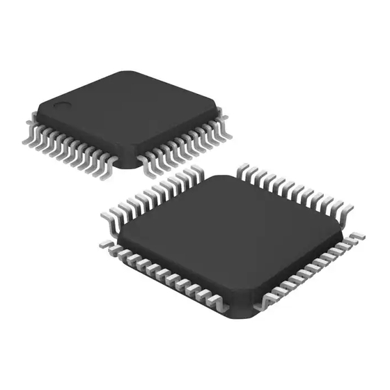
ISD61S00 DESIGN GUIDE 3. PIN CONFIGURATION 47 46 45 44 43 42 41 40 39 38 37 VMID RESET INTB GPIO<14>/RDET VSSD XTALO MCGND ISD61S00 VSSA XTALI VDDL VCCD VSSD VCCA GPIO<13>/RDET DO/GPIO<0> CLK/GPIO<1> VSSA 13 14 15 16 17 18 19 20 21 22 23 24 Figure 3-1 ISD61S00 48-Lead LQFP Pin Configuration. -
Page 13: Pin Description
ISD61S00 DESIGN GUIDE 4. PIN DESCRIPTION Pin Name Function Drive Number RESET Raising this pin to VCC will reset the chip. Active low interrupt request pin. This pin has an INTB 4/8mA open drain output. General Purpose IO Pin or the Ring Detect input GPIO<14>/RDET I/O* 4/8mA... - Page 14 ISD61S00 DESIGN GUIDE GPIO<10> I/O* General Purpose IO Pin. 4/8mA General Purpose IO Pin or the Ring Detect input GPIO<11> I/O* 4/8mA (RDET). GPIO<12> I/O* General Purpose IO Pin. 4/8mA AUXOUT Auxiliary output from PSTN or SPEAKER DAC. VSSA Analog Ground Pin SPKN Negative speaker driver output Negative line driver output...
- Page 15 ISD61S00 DESIGN GUIDE This pin is at VCCD when the chip is ready to RDY/BSYB accept a new command/data and is at VSSD when 4/8mA device is busy. * Default state for digital I/O pins is input with internal pull-up [38Kohms to 83Kohms] to VCCD supply Publication Release Date: March 10, 2011 - 15 - Revision 2.7...
-
Page 16: Block Diagram
ISD61S00 DESIGN GUIDE 5. BLOCK DIAGRAM MIC BIAS MCGND DTMF Generation SPKP SPKN FSK Generation DTMF Detection FSK Detection TI1P TI1N stage1 stage2 TI2P TI2N PO1P PO1N Compression AUXOUT De-Compression I2S Interface Memory Management SPI Interface and Command Flash Memory Controller Interpreter Figure 5-1 ISD61S00 Block Diagram... -
Page 17: Configuration Register Map
ISD61S00 DESIGN GUIDE 6. CONFIGURATION REGISTER MAP Configuration Register Groups Size (Byte) Data memory address Function Usage 0x000 ~ 0x0FF Device Control Registers 0x110 ~ 0x13F Gain stage and Mixer Control Registers 0x140 ~ 0x14F Air CODEC Control 0x150 ~ 0x15F Line CODEC Control 0x160 ~ 0x17F FSK Encoder Control... - Page 18 ISD61S00 DESIGN GUIDE Value Addr. Name Mode Function Reset 0x007 MIC_BIAS 0x00 MIC Interface Bias 8.7.2 0x008 ANA_OUT 0x00 Analog Output Control 8.9.1 8.8.2 0x009 ANA_CTRL 0x10 Analog Control 0x00A ID_OVR 0x00 Memory Control 0x00B PORT_CFG 0x00 GPIO INT Ctrl 8.5.1 8.5.2 0x00C...
- Page 19 ISD61S00 DESIGN GUIDE Value Addr. Name Mode Function Reset 0x02E R7_LSB 0x00 Indirect reg R7 LSB 0x02F 0x00 Indirect reg R7 0x030 PORTB_DO 0x00 Port B Dout 0x031 PORTB_OE 0x00 Port B Output Enable 0x032 PORTB_PE 0xFF Port B Pull Enable 0x033 PORTB_DI Port B Din...
- Page 20 ISD61S00 DESIGN GUIDE Value Addr. Name Mode Function Reset 0x05D REC_MSG_LEN LSB 0x00 REC Message Sector Length [7:0] 0x05E REC_MSG_LEN 0x00 REC Message Sector Length [15:8] 0x110 GS_CTRL 0x00 GS Control 0x111 GS_ACST 0x40 Air CODEC Side tone 0x112 GS_ACIG 0x00 Air CODEC input Gain 0x113...
- Page 21 ISD61S00 DESIGN GUIDE Value Addr. Name Mode Function Reset 0x130 GS_PLIR 0x00 PLAY - I2SR in Gain 0x131 GS_ILIR 0x00 I2SL - I2SR in 0x132 GS_IRIR 0x00 I2SR - I2SR in 0x13B MX_AEC 0x00 AEC Mix Ctrl 0x13C MX_LEC 0x00 LEC Mix Ctrl 0x13D MX_REC...
- Page 22 ISD61S00 DESIGN GUIDE Value Addr. Name Mode Function Reset 0x162 FSKE_FIFO_W FSK Encoder FIFO input 8.12.3 0x163 FSKE_STATUS 0x20 FSK Encoder Status 8.12.4 0x164 FSKE_GAIN 0x39 FSK Encoder Signal Gain 8.12.5 0x165 FSKE_PROG 0x00 FSK Encoder Programmable mode 8.12.6 0x166 FSKE_BAUD_2 0x00 FSK Encoder Baud Rate...
- Page 23 ISD61S00 DESIGN GUIDE Value Addr. Name Mode Function Reset 0x1A0 PWM Clock 0x00 PWM Operation Clock Enable 8.21.1 0x1A2 PWM Tone1 Control 0x00 PWM Tone1 Control 8.21.2 0x1A3 PWM Tone1 Frequency 0x00 PWM Tone1 Frequency 8.21.3 0x1A4 PWM Tone2 Control 0x00 PWM Tone2 Control 8.21.4...
- Page 24 ISD61S00 DESIGN GUIDE Value Addr. Name Mode Function Reset 0x1EA DTMF_RX_DATA 0x00 DTMF Det. Received Data 8.10.10 0x1EB DTMF_RFREQ_MSB 0x00 DTMF Det. Row Frequency MSB 8.10.11 0x1EC DTMF_RFREQ_LSB 0x00 DTMF Det. Row Frequency LSB 8.10.11 0x1ED DTMF_CFREQ_MSB 0x00 DTMF Det. Column Frequency MSB 8.10.12 0x1EE DTMF_CFREQ_LSB...
- Page 25 ISD61S00 DESIGN GUIDE Value Addr. Name Mode Function Reset 0x278 CAS_MIN_HFC 0x01 CAS Min High Frequency Cnt 0x279 CAS_MIN_HFC_LSB 0x21 CAS Min High Frequency Cnt 0x27A CAS_MAX_LFC 0x01 CAS Max Low Frequency Cnt 0x27B CAS_MAX_LFC_LSB 0x5D CAS Max Low Frequency Cnt 0x27C CAS_MIN_LFC 0x01...
- Page 26 ISD61S00 DESIGN GUIDE Value Addr. Name Mode Function Reset 0x30E AEC_DT_SHORT_THRESH_LSB 0x10 AEC Double Talk Detector Parameters 0x30F AEC_DIVERGENCE 0x0F DIVERGENCE THRESHOLD 0x310 AEC_VD_LONG_TC 0x09 AEC Voice Detect Long Time Constant 0x311 AEC_VD_SHORT_TC 0xBB AEC Voice Detect Short Time Constant 0x312 AEC_VD_HANGOVER_TIME_MSB 0x00...
- Page 27 ISD61S00 DESIGN GUIDE Value Addr. Name Mode Function Reset 0x332 AGC_NOISE_THRES_MSB 0x03 AGC NOISE THRESHOLD MSB 0x333 AGC_NOISE_THRES_LSB 0x20 AGC NOISE THRESHOLD LSB 0x334 AGC_MAX_SG 0x02 AGC MAX SG 0x335 AGC_LATK_TC 0xbb AGC LATK TC Constant 0x336 AGC_SATK_TC 0x09 AGC SATK Time Constant 0x338 AEC_VD_SC_CTRL 0x00...
- Page 28 ISD61S00 DESIGN GUIDE Value Addr. Name Mode Function Reset 0x358 AEC_LSOUT[15:8] AEC LSOUT MSB 0x359 AEC_LSOUT[7:0] AEC LSOUT LSB 0x35C AEC_MACRO_ADDR[15:8] 0x00 AEC Macro Address MSB 0x35D AEC_MACRO_ADDR[7:0] 0x00 AEC Macro Address LSB 0x35E AEC_MACRO_DATA[15:8] AEC Macro Data MSB 0x35F AEC_MACRO_DATA[7:0] AEC Macro Data LSB 0x360...
- Page 29 ISD61S00 DESIGN GUIDE Value Addr. Name Mode Function Reset 0x380 LEC_CONFIG 0x96 LEC Configuration 0x381 LEC_RESET 0xA8 LEC Reset 0x382 LEC_EC_BELTA 0x03 LEC EC BELTA 0x383 LEC_AS_COEFF 0x04 LEC AS Coefficient 0x385 LEC_DT_LONG_TC 0x09 LEC Double Talk long term time constant 0x386 LEC_DT_SHORT_TC 0xBB...
- Page 30 ISD61S00 DESIGN GUIDE Value Addr. Name Mode Function Reset 0x3A4 LEC_AS2_MAX_ATTEN_MSB 0x1C LEC AS2 Max Attenuation value(MSB) 0x3A5 LEC_AS2_MAX_ATTEN_LSB 0xA8 LEC AS2 Max Attenuation value(LSB) LEC Noise Suppressor power attack time 0x3A8 LEC_NS_POWER_ATTACK_TC 0xBB constant 0x3A9 LEC_NS_ATTEN_TC 0xBB LEC NS Attenuation Time Constant 0x3AA LEC_NS_ACTIVE_THRESHOLD_MSB 0x03...
- Page 31 ISD61S00 DESIGN GUIDE Value Addr. Name Mode Function Reset 0x3CC LEC_VD_POWER_DEVIATION_MSB LEC VD Power Deviation MSB 0x3CD LEC_VD_POWER_DEVIATION_LSB LEC VD Power Deviation LSB 0x3CE LEC_VD_ACTIVE LEC VD Active 0x3D0 LEC_LRIN[15:8] LEC LRIN MSB 0x3D1 LEC_LRIN[7:0] LEC LRIN LSB 0x3D2 LEC_EOUT[15:8] LEC EOUT MSB 0x3D3 LEC_EOUT[7:0]...
-
Page 32: Device Status
ISD61S00 DESIGN GUIDE 7. DEVICE STATUS Device Status Register Whenever the ISD61S00 receives an SPI command it also returns its current status via MISO. The details of the status byte are shown below. For commands that are not reading digital data from the device this status byte is sent via MISO for every byte of data sent to the ISD61S00. - Page 33 ISD61S00 DESIGN GUIDE 3. READ_INT and check whether any new interrupts have occurred during the service routines. If new interrupt detected go to step 2. The READ_INT will clear the interrupt status. Table 7-2 Interrupt Status Register Description Interrupt Status Byte 1 Bit 7 Bit 6 Bit 5...
-
Page 34: Functional Description
ISD61S00 DESIGN GUIDE TONE_INT The tone or DTMF generator has generated an interrupt. FSK_E The FSK Encoder has generated an interrupt for either half empty or empty condition of FIFO. FSK_D The FSK Decoder has generated an interrupt for a FIFO condition or parity error. CAS_INT The CAS/Arbitrary Tone detector has detected a valid tone. - Page 35 ISD61S00 DESIGN GUIDE SCLK MISO MOSI Figure 8-1 SPI Data Transaction A command transaction begins with sending a command byte (C7-C0). The most significant bit (MSB – C7) is sent in first. During the shift in of the command byte, device status (S7-S0) is sent out MISO. After the command byte, depending upon the command sent, one or more bytes of data may follow.
-
Page 36: Record And Playback Control
ISD61S00 DESIGN GUIDE data was not accepted by the ISD61S00. No further data will be accepted and the host must terminate the SPI transaction. For commands that read data from the part (for instance DIG_READ and SPI_READ) it is not possible to monitor the RDY bit of status so the RDY/BSYB signal must be monitored to know status. - Page 37 ISD61S00 DESIGN GUIDE CMP[4:0] Controls the compression algorithm used for recording. Details in Table 8-1. SR[2:0] Controls the sample rate used for recording. Can also override the playback sample rate. Details in Table 8-2 Table 8-1 COMP_CFG Register Compression Type. Compression Bit rate CMP[4:0]...
-
Page 38: Comp_Ctrl - Compression Control
ISD61S00 DESIGN GUIDE COMP_CTRL – Compression Control 8.2.2 Address Access Mode Value At Reset 0x001 0x00 Bit 7 Bit 6 Bit 5 Bit 4 Bit 3 Bit 2 Bit 1 Bit 0 FIFO Over- FIFO Under- LRMP CFG0_READ PAUSE NRMP SRSIL SRCFG Configuration register CFG1 controls how compressed audio is treated by the compression block:... -
Page 39: Comp_Src - Compression Source
ISD61S00 DESIGN GUIDE COMP_SRC – Compression Source 8.2.3 Address Access Mode Value At Reset 0x002 0x00 Bit 7 Bit 6 Bit 5 Bit 4 Bit 3 Bit 2 Bit 1 Bit 0 Reserved DECODE SPI_IN Reserved Reserved Reserved ENCODE SPI_OUT Output signal data to SPI. -
Page 40: Cfg17 - Update Mode
ISD61S00 DESIGN GUIDE CFG17 – Update Mode 8.2.5 Address Access Mode Value At Reset 0x017 0x01 Bit 7 Bit 6 Bit 5 Bit 4 Bit 3 Bit 2 Bit 1 Bit 0 PLL_LOCK RB_SPI Reserved Reserved COMPRESS UPDATE Immediate update mode. Registers 0x000-0x016 are double buffered. If IMM bit is set register values are active as soon as written. -
Page 41: Phase Locked Loop (Pll) Design Example
ISD61S00 DESIGN GUIDE PLL Prescaler REG44[4] MCLK_DIV REG40[4:2] XTALIN CLKM IMCLK = =R*f 24.576MHz DPLL PLL_BYPASS PLL BLOCK f = 98.304MHz REG44[6] DPLL CODEC_FS BCLK_RATE f/ M REG3[7:4] REG3[3] REG3[2:0] GPIO[13] OPCLK GPIO13 AF bit Master/Slave OPCLK_DIV Mode REG40[1:0] REG50[4] Digital Audio Interface BCLK Figure 8-4 Clock Generation Block Diagram... -
Page 42: Pll_Clk
ISD61S00 DESIGN GUIDE audio, the desired fractional multiplier ratio would be R = 98.304/12.000 = 8.192. This value meets the requirement that the “xy” whole number portion of the multiplier be in the range between 6 and 12. To complete this portion of the design example, the integer portion of the multiplier is truncated to the value, 8. -
Page 43: Pll_Frac
ISD61S00 DESIGN GUIDE 8.3.3 PLL_FRAC Address Access Mode Value At Reset Nominal Value 0x041-0x043 0x000000 Bit7 Bit6 Bit5 Bit4 Bit3 Bit2 Bit1 Bit0 PLL_FRAC [23:16] PLL_FRAC [15:8] PLL_FRAC [7:0] The PLL fractional divider. This 24 bit number represents the fractional part of the PLL PLL_FRAC divider ratio R. -
Page 44: Pcm_Cfg
ISD61S00 DESIGN GUIDE The audio path of the ISD61S00 can generate/accept two channels of audio data. These can be routed to either PCM interface. In addition data can be looped from one PCM interface to the other. The interface has a variety of modes. In I2S mode, PCM interface conforms to the I2S digital audio interface convention where left channel data is active when frame sync is low (WS=0) and right channel when frame sync is high (WS=1). -
Page 45: Pcm_Tslotl
ISD61S00 DESIGN GUIDE 8.4.2 PCM_TSLOTL Address Access Mode Value At Reset 0x051 0x01 Bit 7 Bit 6 Bit 5 Bit 4 Bit 3 Bit 2 Bit 1 Bit 0 TSLOTL[7:0] Left channel PCM data starts TSLOTL clocks after WS rising edge. Bits 9:8 are in TSLOTL[9:0] PCM_COMP0 register. -
Page 46: Pcm_Tslotr1
ISD61S00 DESIGN GUIDE Left channel PCM1 data starts TSLOTL clocks after WS rising edge. Bits 9:8 are in TSLOTL1[9:0] PCM_COMP0 register. 8.4.6 PCM_TSLOTR1 Address Access Mode Value At Reset 0x055 0x11 Bit 7 Bit 6 Bit 5 Bit 4 Bit 3 Bit 2 Bit 1 Bit 0... -
Page 47: Pcm_Tx_Sel
ISD61S00 DESIGN GUIDE TX_L1_SEL[1:0] TX_L ISD61S TX_R TX_L1 RX_L0 MUTE(0) Lout[15:0] SDO1 TX_R1_SEL[1:0] Rout[15:0] TX_R PCM1 TX_L TX_R1 RX_R0 SDI1 MUTE(0) RX_L1 Lin[15:0] RX_R1 Rin[15:0] BCLK I2S_PCM_INF1 TX_L0_SEL[1:0] TX_L TX_L0 TX_R RX_L1 BCLK MUTE(0) Lout[15:0] BCLK BCLK TX_R0_SEL[1:0] Rout[15:0] TX_R PCM0 TX_L TX_R0... -
Page 48: Pcm_Rx_Sel
ISD61S00 DESIGN GUIDE TX_R0_SEL Select what audio to send on right channel of PCM bus TX_L1_SEL Select what audio to send on left channel of PCM1 bus TX_R1_SEL Select what audio to send on right channel of PCM1 bus 8.4.9 PCM_RX_SEL Address Access Mode... -
Page 49: Portx_Ie
ISD61S00 DESIGN GUIDE If this bit is set, and the corresponding PORTA_IE bit, then transitions on PORTA_L_INT PORTA[3:0] will generate a GPIO wakeup interrupt. If this bit is set, and the corresponding PORTA_IE bit, then transitions on PORTA_H_INT PORTA[7:4] will generate a GPIO wakeup interrupt. If this bit is set, and the corresponding PORTB_IE bit, then transitions on PORTB_L_INT PORTB[3:0] will generate a GPIO wakeup interrupt. -
Page 50: Ie1
ISD61S00 DESIGN GUIDE 8.5.4 Address Access Mode Value At Reset Nominal Value 0x015 0xFF Bit7 Bit6 Bit5 Bit4 Bit3 Bit2 Bit1 Bit0 VD_INT RNG_INT CAS_INT FSK_D FSK_E TONE_INT DTMF_INT CPT_INT /TIMER_INT The IE1 register enables the interrupt associated with the bit mask and corresponds to the interrupt status bits in STATUS_REG[2]. -
Page 51: Porta_Di
ISD61S00 DESIGN GUIDE on the state of PORTA_PS. 8.5.8 PORTA_DI Address Access Mode Value At Reset Nominal Value 0x01C 0xFF Bit7 Bit6 Bit5 Bit4 Bit3 Bit2 Bit1 Bit0 PORTA_DI This read only register reflects the state of the GPIO pins of PORTA. PORTA_DI 8.5.9 PORTA_PS... - Page 52 ISD61S00 DESIGN GUIDE This register selects the alternate function of the GPIO pin. PORTA_AF The ports B and C have similar control registers with the following addresses: Register Address (HEX) Register Address (HEX) PORTA_DO PORTB_PS PORTA_OE PORTB_DS PORTA_PE PORTB_AF PORTA_DI PORTC_DO PORTA_PS PORTC_OE...
-
Page 53: Bit Indirect Index Register R0-R7
ISD61S00 DESIGN GUIDE The following ports have alternate functions: Port GPIO Pin Alternate Function Description PORTA<0> GPIO<0> DO pin for external memory access PORTA<1> GPIO<1> CLK pin for external memory access PORTA<4> GPIO<4> I2S Serial Data Out PORTA<5> GPIO<5> I2S WS PORTA<6>... -
Page 54: Microphone Interface And Auxiliary Interface
ISD61S00 DESIGN GUIDE CFG2C R6[7:0] CFG2D R6[15:8] CFG2E R7[7:0] CFG2F R7[15:8] Microphone interface and Auxiliary Interface The ISD61S00 contains a fully integrated programmable microphone interface. No external components other than the microphone are required to operate the circuit. The microphone interface can operate in three modes: 1) Microphone Voltage gain mode;... -
Page 55: Mic_Bias
ISD61S00 DESIGN GUIDE MIC_GAIN[7:4] Set microphone gain in voltage-gain mode. Adjustable voltage gain range: 14dB~37.6dB, 16 steps linear in dB with step size of approximately 1.5dB. Table 8-5 Microphone Gain settings Boosted Boosted MIC_GAIN[7:4] Gain(dB) MIC_GAIN[7:4] Gain(dB) 43.1 30.5 0000 37.65 1000 24.80... - Page 56 ISD61S00 DESIGN GUIDE MIC_RES[7:4] Set microphone bias resistor Table 8-7 Microphone Resistor settings RL (kΩ) RL (kΩ) MIC_RES[7:4] Code 0100 Open 1100 1.25 0101 1101 1.11 0110 1110 0111 3.33 1111 0.91 0000 1000 0.83 0001 1001 0.77 0010 1.67 1010 0.71 0011...
- Page 57 ISD61S00 DESIGN GUIDE Voltage Gain Mode MIC_MODE = 000 Programmable Bias Generator MIC_BIAS[2:0] MIC_RES[7:4] 2.436V MIC_GAIN[7:4] MIC_GAIN[7:4] MCGND Figure 8-6 Microphone Voltage Gain Mode For higher gain configurations, the current gain mode can be used. Figure 8-7 Microphone Current Gain Mode shows how the current gain mode is used.
- Page 58 ISD61S00 DESIGN GUIDE Current Gain Mode MIC_MODE = 010 or 011 Programmable Bias Generator MIC_BIAS[2:0] MIC_RES[7:4] 2.436V MIC_GAIN[7:4] mode mode MCGND Figure 8-7 Microphone Current Gain Mode The value of R feedback resistor for mode 010 is shown below.
- Page 59 ISD61S00 DESIGN GUIDE The voltage gain from MCP to MCO can be expected in the range of 29 to 55dB with a standard electret microphone and a microphone bias resistor set to 10K Ohm (MIC_RES[7:4]=0x05) The voltage gain from MCP to MCO can be expected in the range of 26 to 49dB with a standard electret microphone and a microphone bias resistor set to 0.67K Ohm (MIC_RES[7:4]=0x0B) One should note that the gain depends on the microphone internal characteristics and part number.
-
Page 60: Pstn Analog Input
ISD61S00 DESIGN GUIDE Auxillary Gain Mode MIC_MODE = 101 Programmable Bias Generator MIC_BIAS[2:0] MIC_RES[7:4] 2.436V MIC_GAIN[7:4] mode MCGND Figure 8-9 Auxiliary Input Mode PSTN Analog Input The PSTN analog input consists of two multiplexed pins to allow on-hook CID snooping along with normal off-hook operation. -
Page 61: Ti_Gain
ISD61S00 DESIGN GUIDE TI1P TI1P TI2P TI_G1 =10K, 20K, TI_G2 =10K, 20K, 40K 40K, 80K 80K, 160K TI2P TI3P STG1 STG2 TI1N TI1N TI2N TI2N TI3N TI_G1 =10K, 20K TI_G2 =10K, 20K, 40K 40K, 80K 80K, 160K Figure 8-10 TI Input Amplifier 8.8.1 TI_GAIN Address... - Page 62 ISD61S00 DESIGN GUIDE First stage selection TI_S1[1] TI_S1[0] input selected Don‟t use none Select TI1 pins Select TI2 pins Select PO pins Second stage selection TI_S2[1] TI_S2[0] input selected Output of stage 1 default Select TI1 pins Select TI2 pins Select TI3 pins * When this mode is selected the PO+ PO- pins are internally connected to the input of the PSTN analog interface.
-
Page 63: Analog Outputs
ISD61S00 DESIGN GUIDE Table 8-8 TI Gain Settings TI_G1[1:0] TI_G2[2:0] Gain [dB] Gain [dB] 0 dB 0 dB 6 dB 6 dB 12 dB 12 dB 18 dB 18 dB 24 dB Table 8-9 TI MUX Settings TI_S1[1:0] TI_S2[1:0] Input Input None STG1... -
Page 64: Ana_Out
ISD61S00 DESIGN GUIDE 8.9.1 ANA_OUT Address Access Mode Value At Reset 0x008 0x00 Bit 7 Bit 6 Bit 5 Bit 4 Bit 3 Bit 2 Bit 1 Bit 0 PO_EN PO_GAIN SPK_EN SPK_GAIN SPK_GAIN Set speaker driver gain SPK_EN = 0 Disable (power down) speaker DAC = 1 Enable speaker DAC PO_GAIN Set line driver gain... - Page 65 ISD61S00 DESIGN GUIDE PU_SPK = 0 power down = 1 power up PU_PO = 0 power down = 1 power up 8.10 DTMF Detection Dual Tone Multi Frequency (DTMF) signals consist of a sum of two tones: a low tone of 697Hz, 770Hz, 852Hz or 941Hz (row tone) and a high tone of 1209Hz, 1336Hz, 1477Hz or 1633Hz (column tone) as shown in Table 8-10.
- Page 66 ISD61S00 DESIGN GUIDE DTMF tone 770Hz & 1336Hz ( From line ) ROW tone ( From Biquad ) ROWdet COL tone ( From Biquad ) COLdet DTMF_State ( ROWdet & COLdet ) ACCT DTMF_RDY DTMF_Rx_Data Figure 8-13 DTMF Detector Acquisition Timing Table 8-10 DTMF Tone Decoding Column frequency 1209 Hz...
-
Page 67: Dtmf_Ctrl
ISD61S00 DESIGN GUIDE 8.10.1 DTMF_CTRL Address Access Mode Value At Reset Nominal Value 0x1E0 0x00 Bit7 Bit6 Bit5 Bit4 Bit3 Bit2 Bit1 Bit0 DTMF_EN Reserved DTMF_FREQ_DEV DTMF_TC DTMF_TC Sets the time constant used for DTMF signal energy level estimation. The DTMF_TC constant controls the speed at which the energy converges. -
Page 68: Dtmf_Fifo
ISD61S00 DESIGN GUIDE 8.10.3 DTMF_FIFO Address Access Mode Value At Reset Nominal Value 0x1E2 0x00 Bit7 Bit6 Bit5 Bit4 Bit3 Bit2 Bit1 Bit0 FIFO_DEPTH FIFO_DATA FIFO_DATA A read to this register reads back the head of the FIFO and increments read pointer to next address. -
Page 69: Dtmf_Pdt
ISD61S00 DESIGN GUIDE 8.10.6 DTMF_PDT Address Access Mode Value At Reset Nominal Value 0x1E6 0x00 Bit7 Bit6 Bit5 Bit4 Bit3 Bit2 Bit1 Bit0 DTMF_PDT This is the Present Detect Time, the time for which a tone must be present to be DTMF_PDT qualified as a valid DTMF tone. -
Page 70: Dtmf_Adt
ISD61S00 DESIGN GUIDE 8.10.7 DTMF_ADT Address Access Mode Value At Reset Nominal Value 0x1E7 0x00 Bit7 Bit6 Bit5 Bit4 Bit3 Bit2 Bit1 Bit0 DTMF_ADT This is the Absent Detect Time, the time for which a tone must be absent before a DTMF_ADT signal is considered a new DTMF tone. -
Page 71: Dtmf_Row_Freq
ISD61S00 DESIGN GUIDE 8.10.11 DTMF_ROW_FREQ Address Access Mode Value At Reset Nominal Value 0x1EB-0x1EC 0x0000 Bit7 Bit6 Bit5 Bit4 Bit3 Bit2 Bit1 Bit0 DTMF Row Frequency [15:8] DTMF Row Frequency [7:0] DTMF_ROW_FREQ[15:3] is the integer part of the DTMF Row frequency, DTMF DTMF_ROW_FREQ[2:0] is the decimal fraction part of the DTMF Row frequency (13.3 format). -
Page 72: Dtmf And Arbitrary Tone Generation
ISD61S00 DESIGN GUIDE 8.11 DTMF and Arbitrary Tone Generation. The ISD61S00 has two independently programmable voice-band oscillators for DTMF and FSK tone generation. The tone generators can be controlled by individual registers or automatically by the DTMF or FSK generation sub-systems. FREQ_A SPI Interface FREQ_B... -
Page 73: Tone_Ctrl
ISD61S00 DESIGN GUIDE Don‟t Continuous User defined User defined Set : 0 Set : 0 Set : 0 Mode care Don‟t care DTMF Mode User defined User defined User defined Number of digits Digits to in tone index send registers. Don‟t Programmable User defined... -
Page 74: Tone_Freq_B
ISD61S00 DESIGN GUIDE 8.11.3 TONE_FREQ_B Address Access Mode Value At Reset Nominal Value 0x1C3-0x1C4 0x0000 Bit7 Bit6 Bit5 Bit4 Bit3 Bit2 Bit1 Bit0 Reserved TONE_FREQ_B[14:8] TONE_FREQ_B[7:0] TONE_FREQ_B Sets the frequency of tone B to TONE_FREQ_B * 2.5 Hz. If set to zero, tone B is disabled. -
Page 75: Tone_Off_Time
ISD61S00 DESIGN GUIDE 8.11.7 TONE_OFF_TIME Address Access Mode Value At Reset Nominal Value 0x1C8 0x00 Bit 7 Bit 6 Bit 5 Bit 4 Bit 3 Bit 2 Bit 1 Bit 0 TONE_OFF_TIME TONE_OFF_TIME It sets the absent (off) time between each tone to TONE_OFF_TIME * 1ms. Set to zero for continuous mode. -
Page 76: Tone_Index_0 ~ Tone_Index_A
ISD61S00 DESIGN GUIDE 8.11.10 TONE_INDEX_0 ~ TONE_INDEX_A Address Access Mode Value At Reset Nominal Value 0x1D0-0x1DB 0x00 Bit7 Bit6 Bit5 Bit4 Bit3 Bit2 Bit1 Bit0 Digit 0 Digit 1 Digit 2 Digit 3 Digit 4 Digit 5 Digit 6 Digit 7 Digit 8 Digit 9 Digit 10... - Page 77 ISD61S00 DESIGN GUIDE The ISD61XX provides an FSK generator supporting Bell 202, Bell 103, ITU-T V.23 and ITU-T V.21 standard FSK. The FSK Generator controls the tone generator to generate phase continuous tones at the appropriate frequency and baud rate. The generator can be configured to package bytes with selectable start and stop bits and a parity bit.
-
Page 78: Fske_Ctrl1
ISD61S00 DESIGN GUIDE 8.12.1 FSKE_CTRL1 Address Access Mode Value At Reset Nominal Value 0x160 0x00 Bit 7 Bit 6 Bit 5 Bit 4 Bit 3 Bit 2 Bit 1 Bit 0 FSK_EN PACKAGE_EN HALF_FIFO_INT FSK_TX_ON STOP_SEL RESERVED FSK_EN 1: Enable FSK encoder. 0: Power down FSK encoder. PACKAGE_EN 1: Package mode. -
Page 79: Fske_Tx_Data
ISD61S00 DESIGN GUIDE 300 bps 300 bps Baud 1200 1200 300 bps 300 bps Rate 110 bps 110 bps Mark ‘1’ 390Hz 1300Hz 387Hz 1200Hz 1270Hz 2225Hz 980Hz 1650Hz Space ‘0’ 450Hz 2100Hz 487Hz 2200Hz 1070Hz 2025Hz 1180Hz 1850Hz 8.12.3 FSKE_TX_DATA Address Access Mode Value At Reset... -
Page 80: Fske_Baud (Sw_Mode = 1)
ISD61S00 DESIGN GUIDE Address Access Mode Value At Reset Nominal Value SW_MODE RESERVED RESERVED RESERVED RESERVED RESERVED RESERVED SW_FLT SW_MODE When set, SPEC_SEL is ignored and the FSK encoder frequencies and baud rate are controlled by FSKE_MARK_FREQ, FSKE_SPACE_FREQ, and FSKE_BAUD described below. -
Page 81: Fske_Space_Freq (Sw_Mode = 1)
ISD61S00 DESIGN GUIDE 8.12.9 FSKE_SPACE_FREQ (SW_MODE = 1) Address Access Mode Value At Reset Nominal Value 0x16B~0x16C 0x00 Bit 7 Bit 6 Bit 5 Bit 4 Bit 3 Bit 2 Bit 1 Bit 0 RESERVED SPACE_FREQ[14:8] SPACE_FREQ[7:0] SPACE_FREQ In SW_MODE these registers determine the space frequency of the generated FSK. Frequency is given by SPACE_FREQ * 2.5Hz. - Page 82 ISD61S00 DESIGN GUIDE byte bNumChanSeizeBytes = NUM_SEIZE; byte bNumMarkBytes = NUM_MARK; switch(byFSKGenState) case FSKG_IDLE: if(bUsbCtrl[0] & USB_CTRL0_FSK_GEN_START) byFSKGenState = FSKG_CHANNEL_SEIZURE; break; case FSKG_CHANNEL_SEIZURE: // The assumption here is that the FSK encoder block // general configuration has been setup already now // we just turn off package mode and send channel seizure // signal.
- Page 83 ISD61S00 DESIGN GUIDE byCounter = 0; break; case FSKG_CHANNEL_SEIZURE2: if(DevStatus[2] & STATUS2_FSK_E) // We get here FIFO interrupt has occurred. There is space for // at least 4 bytes (half interrupt set) if(bNumChanSeizeBytes > 3) // Load 4 bytes into FSK FIFO for (i=0;i<4;i++) writeCfgReg(CFG_FSKE_FIFO_W,0x55);...
- Page 84 ISD61S00 DESIGN GUIDE // Load bytes into FSK FIFO for (i=0;i< bNumMarkBytes;i++) writeCfgReg(CFG_FSKE_FIFO_W,0xFF); writeCfgReg(CFG_FSKE_FIFO_W,0xFF); // Ensure that next INT is for FIFO empty tmp = ReadRegister(CFG_FSKE_CTRL1); tmp &= ~CFG_FSKE_CTRL1__HALF_FIFO_INT; writeCfgReg(CFG_FSKE_CTRL1,tmp); byCounter = 0; byFSKGenState = FSKG_DATA_CONFIG; bNumMarkBytes = 0; break; case FSKG_DATA_CONFIG: if(DevStatus[2] &...
-
Page 85: Fsk Detection
ISD61S00 DESIGN GUIDE for (i=0;i<tmp;i++) writeCfgReg(CFG_FSKE_FIFO_W,TxDataFifo.Fifo_Buffer[(TxDataFifo.ReadIndex++ & 0x3F)]); TxDataFifo.Depth -= tmp; else if(TxDataFifo.Depth) // There are more bytes to Tx for (i=0;i<TxDataFifo.Depth;i++) writeCfgReg(CFG_FSKE_FIFO_W,TxDataFifo.Fifo_Buffer[(TxDataFifo.ReadIndex++ & 0x3F)]); TxDataFifo.Depth -= TxDataFifo.Depth; else // Only get to here if TxDataFIFO is empty. Check for EOT // condition which is USB_CTRL0_FSK_GEN_START set low. -
Page 86: Fskd_Ctrl
ISD61S00 DESIGN GUIDE .The system consists of filtering the incoming signal followed by a match filter to extract FSK data. Additional blocks perform carrier detection and clock recovery to synchronize the data and load it into a FIFO for host processing. The match filter consists of a shift register sampling the signal at 48kHz. This sampled waveform is compared to the matching templates impulse_L and impulse_H for the mark and space frequencies each sample period. - Page 87 ISD61S00 DESIGN GUIDE Address Access Mode Value At Reset Nominal Value FSK_EN CDB_DET_MD MARK_DET RESERVED RESERVED RESERVED RESERVED FSK_INT_MD FSK_INT_MD 1: The FSK interrupt will only occur when a 0x55 or 0xAA byte is detected; this mode is used for detecting channel seizure signal. 0: The FSK interrupt will occur normally;...
-
Page 88: Fskd_Mode
ISD61S00 DESIGN GUIDE 8.13.2 FSKD_MODE Address Access Mode Value At Reset Nominal Value 0x181 0x04 Bit 7 Bit 6 Bit 5 Bit 4 Bit 3 Bit 2 Bit 1 Bit 0 Reserved Reserved PARITY_EN PARITY_TYPE MODE[3:0] PARITY_EN When set decoder expects a parity bit in the received data following the 8 data bits. Parity error status is reported in bit 3 of FSKD_FIFO_STATUS (0x18B). -
Page 89: Fskd_Status
ISD61S00 DESIGN GUIDE CORR_ADJ_S Match filter space frequency correlation adjust value polarity. 0: increase space correlation. 1: decrease space correlation. CF_ADJ_SW Carrier frequency detect count for software mode. When set the default carrier detect frequency values are over-ridden and CDB_FREQ_LOW_CNT (0x190-0x191) CDB_FREQ_HIGH_CNT (0x192-0x193) registers are used to determine CDB frequency detection. -
Page 90: Fskd_Judge
ISD61S00 DESIGN GUIDE scale input peak-to-peak voltage at the ADC which is Avdd V. To refer to input voltage, adjust for the TI input gain. 8.13.6 FSKD_JUDGE Address Access Mode Value At Reset Nominal Value 0x0186 0x04 Bit 7 Bit 6 Bit 5 Bit 4 Bit 3... -
Page 91: Fskd_Fifo_Ctrl
ISD61S00 DESIGN GUIDE CDB_TIME[5:0] Determines the time before CDB (Carrier Detect Bar) goes low. Time is given by 8*CDB_TIME ms. Carrier Detection The carrier detection block determines whether there is an FSK carrier present on the input signal. The circuit examines an 8ms time slice and determines whether a carrier is present. CDB (Carrier Detect Bar) will go low under either of the following situations: 1. -
Page 92: Fskd_Fifo_Dout
ISD61S00 DESIGN GUIDE 8.13.10 FSKD_FIFO_DOUT Address Access Mode Value At Reset Nominal Value 0x18A 0x00 Bit 7 Bit 6 Bit 5 Bit 4 Bit 3 Bit 2 Bit 1 Bit 0 FSKD_FIFO_DOUT FSKD_FIFO_DOUT Received data stored in FIFO. The FIFO depth is 8 bytes. If FIFO is not read after a FIFO FULL condition then next data received will be lost. -
Page 93: Fskd_Energy_Low_Th
ISD61S00 DESIGN GUIDE 8.13.13 FSKD_ENERGY_LOW_TH Address Access Mode Value At Reset Nominal Value 0x18D 0x06 Bit7 Bit6 Bit5 Bit4 Bit3 Bit2 Bit1 Bit0 FSKD_ENERGY_LOW_TH[7:0] FSKD_ENERGY_LOW_TH[7:0] Used for Bell202, V.23 type1 standard. Sets the FSK carrier off energy low threshold. Detector will enter carrier off condition when FSK signal power is under this level for 2*FSKD_ENERGY_TC*1/16K seconds. -
Page 94: Fskd_Cdb_Freq_High_Cnt
ISD61S00 DESIGN GUIDE 8.13.17 FSKD_CDB_FREQ_HIGH_CNT Address Access Mode Value At Reset Nominal Value 0x192~0x193 0x23F5 Bit7 Bit6 Bit5 Bit4 Bit3 Bit2 Bit1 Bit0 FSKD_CDB_FREQ_HIGH_CNT[15:8] FSKD_CDB_FREQ_HIGH_CNT[7:0] FSKD_CDB_FREQ_HIGH_CNT CDB high frequency detect count. Valid only when CF_ADJ_SW (0x182) is 1. The formula for CDB_FREQ_CNT is: 12288000 ... -
Page 95: Example Fsk Detector Usage
ISD61S00 DESIGN GUIDE Figure 8-17 band pass filter frequency response 8.13.19 Example FSK Detector Usage Usage of the FSK detector normally involves three steps: 1. Configure the detector. 2. Detect channel seizure. 3. Receive transmitted data. // Configure Input path: Enable a TI input and set input gain. writeCfgReg(CFG_TI_GAIN,0x0a);... - Page 96 ISD61S00 DESIGN GUIDE writeCfgReg(CFG_FSKD_ENERGY_TC,0x40); Below is the Evaluation board interrupt service routine for reference. When triggered the state machine looks for a carrier synchronization signal then receives data to a FIFO. A 10ms timer tick is assumed in operation and correct path and specification configuration. PUBLIC void vFSKDetFSM(void) static byte byCounter;...
- Page 97 ISD61S00 DESIGN GUIDE else if((DevStatus[3] & STATUS3_TIMER_INT) && (bUsbStatus[4] & USB_STATUS4__FSK_DETECTED)) // Timer interrupt has occurred tmp = ReadRegister(CFG_FSKD_FIFO_STATUS); if(!(tmp & CFG_FSKD_FIFO_STATUS__EMPTY)) // If FIFO is not empty tmp = ReadRegister(CFG_FSKD_FIFO_DOUT); writeCfgReg(CFG_FSKD_FIFO_CTRL,CFG_FSKD_FIFO_CTRL__CLEAR + 0x30); byCounter = 0; break; byCounter++; // We wait 50ms without a FIFO interrupt then assume that we have // finished synchronization if(byCounter >...
- Page 98 ISD61S00 DESIGN GUIDE else if(DevStatus[3] & STATUS3_TIMER_INT) // We are here due to a timer tick. This means we may be finished with // transmission. byCounter++; // We wait 50ms without a FIFO interrupt then we may have // finished data transmission if(byCounter >...
-
Page 99: Cas And Arbitrary Tone (Atd) Detector
ISD61S00 DESIGN GUIDE break; // Setup channel seizure detection OrCfgReg(CFG_FSKD_CTRL,0x01); AndCfgReg(CFG_FSKD_MODE,~0x20); // Wait for INT for carrier detection. // Read off data from FIFO of channel seizure or wait until channel seizure time has // elapsed then reset FIFO. Channel now transmits STOP (MARK) signal for some period // Change mode to appropriate packaged mode. - Page 100 ISD61S00 DESIGN GUIDE CAS Detector 2130 Hz High Threshold Biquad Part sinc Guard £U_£G MODout ALGO Input Filter Time fs=1.536MHz Low Threshold 2750 Hz Part Biquad : High Threshold comparator : Low Threshold comparator Figure 8-18 Block Diagram of CAS Detection The CAS detector consists of two biquad bandpass filters to extract the high and low tones of the CAS signal.
-
Page 101: Cas_Ctrl
ISD61S00 DESIGN GUIDE Figure 8-20 CAS Detector Biquad High Tone Frequency Response The CAS detector can also be programmed as an arbitrary tone detector (ATD). In ATD mode coefficients for the low and high tone biquad filters are provided by the user. The frequency specifications and deviation are also programmed by the user. -
Page 102: Cas_Thres_Low - Cas Detector Low Threshold
ISD61S00 DESIGN GUIDE Table 8-17 CAS Detector Frequency Deviation Control. FREQ_DEV[1:0] % Dev High Tone 2805~2695 Hz 2777~2722 Hz 2805~2695 Hz 2832~2667 Hz 2750 Hz Low Tone 2176~2087 Hz 2151~2109 Hz 2176~2087 Hz 2193~2066 Hz 2130 Hz 8.14.2 CAS_THRES_LOW – CAS detector low threshold Address Access Mode Value At Reset... -
Page 103: Cas_Present
ISD61S00 DESIGN GUIDE CAS signal. MULT [3:0] The CAS/ATD detector processes two thresholds, CAS_THRES_LOW and CAS_THRES_HIGH. CAS_THRES_HIGH is calculated by CAS_THRES_LOW << MULT. For example above and MULT=4 CAS_THRES_HIGH = 8 mV =128 mV If (CAS_THRES_LOW << MULT) ≥ 0x7FFF, CAS_THRES_HIGH saturates to 0x7FFF. -
Page 104: Cas_Absent
ISD61S00 DESIGN GUIDE 8.14.5 CAS_ABSENT Address Access Mode Value At Reset Nominal Value 0x205 0x20 Bit 7 Bit 6 Bit 5 Bit 4 Bit 3 Bit 2 Bit 1 Bit 0 CAS_ABSENT_TIME CAS_ABSENT_TIME [7:0] This is the time a detected CAS/ATD tone must be absent before removal of CAS_DET signal. -
Page 105: Atd_Max_Hfc (Atd_Mode = 1)
ISD61S00 DESIGN GUIDE 00: dual-tone mode 01: detect low tone only when ATD_MODE=1 DET_MODE 10: detect high tone only when ATD_MODE=1 11: detect high/low tone separately when ATD_MODE=1 Number of sine wave periods to be used for frequency calculations. The more cycles the higher the frequency accuracy but the more computation time required. -
Page 106: Atd_Max_Lfc (Atd_Mode = 1)
ISD61S00 DESIGN GUIDE the frequency of sampling clock defined by register det_rsol. 8.14.10 ATD_MAX_LFC (ATD_MODE = 1) Address Access Mode Value At Reset Nominal Value 0x020C-0x20D 0x0161 Bit 7 Bit 6 Bit 5 Bit 4 Bit 3 Bit 2 Bit 1 Bit 0 RESERVED RESERVED... -
Page 107: Fsk_Coeff - Fsk Encoder Coefficient Ram Data
ISD61S00 DESIGN GUIDE Address Access Mode Value At Reset Nominal Value 0x0242~0273 0x00 Bit 7 Bit 6 Bit 5 Bit 4 Bit 3 Bit 2 Bit 1 Bit 0 ATD_LF_COEFF ATD_HF_COEFF IIR filter coefficients the high tone arbitrary tone detector. ATD_LF_COEFF IIR filter coefficients the low tone arbitrary tone detector. -
Page 108: Fsk_Coeff_Addr - Fsk Encoder Coefficient Ram Address
ISD61S00 DESIGN GUIDE Biq-1 Biq-2 Biq-3 Biq-4 Biq-1 Biq-2 Biq-3 Biq-4 Ext-Coeff Figure 8-23 FSK encoder IIR filter structure In order to program this ram, 0x0200[7] CAS_EN must be set, and 0x0200[6] IIR_EN must be clear The parameter is 16 bits long with 3.13 format, and user must write high byte first then low byte. 0x0275[0]=0 is the high byte, and 0x0275[0] =1 is the low byte. -
Page 109: Cas_Min_Hfc (Fine_Tune = 1)
ISD61S00 DESIGN GUIDE This is the maximum frequency count for the high tone arbitrary frequency detector. A tone is detected when the frequency counter falls between CAS_MIN_HFC and CAS_MAX_HCF. The value CAS_MAX_HFC of this register should be set to: = (48000 * 16) / (Desired_High_Frequency * (1+ error%)) CAS_MAX_HFC 8.14.16 CAS_MIN_HFC (FINE_TUNE = 1) Address... -
Page 110: Arbitrary Tone Detector Example
ISD61S00 DESIGN GUIDE This is the minimum frequency count for the high tone arbitrary frequency detector. A tone is detected when the frequency counter falls between CAS_MIN_HFC and CAS_MAX_HCF. The value CAS_MIN_LFC of this register should be set to: CAS_MIN_LFC = (48000 * 16) / (Desired_low_tone_Frequency * (1- error%)) 8.14.19 8.14.20... - Page 111 ISD61S00 DESIGN GUIDE writeCfgReg(CFG_ATD_MAX_LFC_LSB,0x14); writeCfgReg(CFG_ATD_MIN_LFC,0x02); writeCfgReg(CFG_ATD_MIN_LFC_LSB,0x36); // Biquad coefficients for 2300 and 1400Hz writeCfgReg(0x211,0x03); writeCfgReg(0x214,0xd8); writeCfgReg(0x215,0xd8); writeCfgReg(0x216,0xff); writeCfgReg(0x217,0xfc); writeCfgReg(0x218,0x1f); writeCfgReg(0x219,0x39); writeCfgReg(0x21a,0x20); writeCfgReg(0x21c,0xda); writeCfgReg(0x21d,0xf6); writeCfgReg(0x21e,0xd9); writeCfgReg(0x21f,0x61); writeCfgReg(0x220,0x20); writeCfgReg(0x222,0x1f); writeCfgReg(0x223,0x75); writeCfgReg(0x224,0x20); writeCfgReg(0x226,0xd5); writeCfgReg(0x227,0xf7); writeCfgReg(0x228,0xd8); writeCfgReg(0x229,0x08); writeCfgReg(0x22a,0x1f); writeCfgReg(0x22b,0xff); writeCfgReg(0x22c,0x1f); writeCfgReg(0x22d,0x78); writeCfgReg(0x22e,0x20); writeCfgReg(0x230,0xda); writeCfgReg(0x231,0x08); writeCfgReg(0x232,0xd9);...
- Page 112 ISD61S00 DESIGN GUIDE writeCfgReg(CFG_TIME_CTRL,0x80); break; case CONTID_HANDSHAKE0: // This is first stage of detecting ContactID handshake a // 1400Hz tone. if(DevStatus[2] & STATUS2_CAS_INT){ tmp = ReadRegister(CFG_CAS_STATUS); if(tmp == CFG_CAS_STATUS__LOW_TONE){ // Change timer to 10msec writeCfgReg(CFG_TIME_CTRL,0x00); writeCfgReg(CFG_TIME_TARG,0x00); writeCfgReg(CFG_TIME_TARG_LSB,0x09); writeCfgReg(CFG_TIME_CTRL,0x80); byCounter = 0; byContactIDState = CONTID_HANDSHAKE1;...
- Page 113 ISD61S00 DESIGN GUIDE break; case CONTID_DELAY_TO_TX: if(DevStatus[3] & STATUS3_TIMER_INT){ // Timer interrupt has occurred byCounter++; if(byCounter > 199){ // 200 millisecond delay until transmit byContactIDState = CONTID_TRANSMIT0; break; case CONTID_TRANSMIT0: // If there is Contact ID data on FIFO to // transmit, start transmission.
- Page 114 ISD61S00 DESIGN GUIDE // Detecting 1400Hz Kiss-off tone. if(DevStatus[2] & STATUS2_CAS_INT){ tmp = ReadRegister(CFG_CAS_STATUS); if(tmp == CFG_CAS_STATUS__LOW_TONE){ byCounter = 0; // Setup to generate tone OFF interrupt writeCfgReg(CFG_CAS_CTRL, CFG_CAS_CTRL__TONE_OFF_INT + CFG_CAS_CTRL__IRR_EN + CFG_CAS_CTRL__CAS_EN); byContactIDState = CONTID_KISSOFF1; else if(DevStatus[3] & STATUS3_TIMER_INT) // Timer interrupt has occurred byCounter++;...
-
Page 115: Voice Energy Detection (Speech Energy Detection)
ISD61S00 DESIGN GUIDE writeCfgReg(CFG_TIME_CTRL,0x80); byCounter = 0; byContactIDState = CONTID_DELAY_TO_TX; break; case CONTID_WAIT_IDLE: if(!(bUsbCtrl[0] & USB_CTRL0_CONTID_START)){ byContactIDState = CONTID_IDLE; break; default: byContactIDState = CONTID_IDLE; break; 8.15 Voice Energy Detection (Speech Energy Detection) The voice energy detector allows measurement of signal energy in the voice band between 750Hz to 1400Hz. -
Page 116: Vd_Ctrl
ISD61S00 DESIGN GUIDE 8.15.1 VD_CTRL Address Access Mode Value At Reset Nominal Value 0x1F0 0x00 Bit7 Bit6 Bit5 Bit4 Bit3 Bit2 Bit1 Bit0 VD_EN Reserved Reserved Reserved VD_TC [3:0] VD_TC[3:0] Voice Detect TC (time constant) determines the response of the voice detect energy averaging. -
Page 117: Call Progress Tone Detector
ISD61S00 DESIGN GUIDE VD_ENERGY[15:0] This register represents the instantaneous signal power from 750Hz to 1400Hz. The value is in the range, 0x0000 to 0xFFFF, with larger value representing larger signal power. 8.16 Call Progress Tone Detector The call progress tone detector is a narrow band pass filter from 300Hz to 650Hz; its detection algorithm is similar to voice energy detection. -
Page 118: Cpt_Status
ISD61S00 DESIGN GUIDE 8.16.2 CPT_STATUS Address Access Mode Value At Reset Nominal Value 0x281 0x00 Bit7 Bit6 Bit5 Bit4 Bit3 Bit2 Bit1 Bit0 Reserved Reserved Reserved Reserved Reserved Reserved Reserved CPT_RX CPT_RX Call Progress Tone Detected. 1: Energy exceeds CPT_THRES_H 0: Energy less than CPT_THRES_L or CPT_EN=0. -
Page 119: Cpt_Energy
ISD61S00 DESIGN GUIDE 8.16.5 CPT_ENERGY Address Access Mode Value At Reset Nominal Value 0x286~0x287 0x0000 Bit7 Bit6 Bit5 Bit4 Bit3 Bit2 Bit1 Bit0 CPT_ENERGY [15:8] CPT_ENERGY [7:0] CPT_ENERGY[15:0] This register represents the instantaneous signal power from 300Hz to 650Hz. The value is in the range, 0x0000 to 0xFFFF, with larger value representing larger signal power. -
Page 120: Rng_Ctrl
ISD61S00 DESIGN GUIDE 12.288MHz Prescale Resolution_time 12KHz reset 16 bits RINGCNTR counter Ringing signal / RING_in reset interrupt logic RINGIntrpt RING_State interrupt Occurrence register Figure 8-26 Block diagram of ring detector RNG_in RNG_in RNG_in RINGintrpt RINGintrpt RINGintrpt Resolution_time Resolution_time Resolution_time RINGCNTR [15:0] RINGCNTR [15:0] RINGCNTR [15:0]... - Page 121 ISD61S00 DESIGN GUIDE INT_SEL[0] Generates an interrupt on falling edge. INT_SEL[1] Generates an interrupt on rising edge. Address=0x01B0 Interrupt Occurrence Bit[1] Bit[0] No Interrupt Interrupt on falling edge Interrupt on rising edge Interrupt on both falling and rising edge Table 8-19 Values of PPM Timer resolution. RES[1:0] Resolution Time Unit 1/12KHz = 83us...
-
Page 122: Rng_State
ISD61S00 DESIGN GUIDE 8.17.2 RNG_STATE Address Access Mode Value At Reset Nominal Value 0x01B1 0x00 Bit 7 Bit 6 Bit 5 Bit 4 Bit 3 Bit 2 Bit 1 Bit 0 RESERVED RESERVED RESERVED RESERVED RESERVED RESERVED RESERVED RING_STATE RING_STATE This bit reflects the state of ringing signal passing through the Schmitt trigger input pad. -
Page 123: Rng_Latch
ISD61S00 DESIGN GUIDE PPM counter, max (16 bit counter)=65535 ( PPM counter value= PPM counter operating frequency / Frequency) 8.17.4 RNG_LATCH Address Access Mode Value At Reset Nominal Value 0x1B4 0x00 Bit 7 Bit 6 Bit 5 Bit 4 Bit 3 Bit 2 Bit 1 Bit 0... -
Page 124: Time_Targ
ISD61S00 DESIGN GUIDE 8.18.2 TIME_TARG Address Access Mode Value At Reset Nominal Value 0x292~0x293 0x0000 Bit7 Bit6 Bit5 Bit4 Bit3 Bit2 Bit1 Bit0 TIME_TARG[15:8] TIME_TARG[7:0] TIME_TARG[15:0] TIME_TARG+1 ms timer target count, maximum count 65536 ms. 8.18.3 TIME_CNT Address Access Mode Value At Reset Nominal Value 0x294~0x295... - Page 125 ISD61S00 DESIGN GUIDE TONE PLAY MIX_OUT I2SL I2SR Figure 8-28 Gain/Mixer Channel In addition to the mixers there are also gain stages associated with each of the CODECs and echo cancellers that allow input and output gain control along with side tone insertion. Lrin Asout To Mixer...
- Page 126 ISD61S00 DESIGN GUIDE corresponding to a total MUTE of the signal as shown in Table 8-20. The list of mixer gain registers and their associated path is given in Table 8-21. Table 8-20 Gain Stage Control value Mapping. Index Gain (dB) Index Gain (dB) Index...
- Page 127 ISD61S00 DESIGN GUIDE Table 8-21 Mixer Gain Registers. Register Description Address Register Description Address GS_ACST Air CODEC Side tone GS_ILLI I2SL - LEC in GS_ACIG Air CODEC input Gain GS_IRLI I2SR - LEC in GS_ACOG Air CODEC output Gain GS_AORI AEC out - REC in Gain GS_AEOG AEC Output Gain...
-
Page 128: Gs_Ctrl
ISD61S00 DESIGN GUIDE Lrin Asout TONE TONE PLAY PLAY AECin Lsout Arin I2SLin TONE I2SL I2SL DTMF Detection PLAY I2SR I2SR FSK Detection Lrin Asout TONE TONE I2SL I2SR PLAY PLAY Lsout Arin LECin I2SRin I2SL I2SL... -
Page 129: Codec Ec Gain Stages
ISD61S00 DESIGN GUIDE 8.19.2 CODEC EC Gain Stages Address Access Mode Value At Reset Nominal Value 0x111-0x119 0x00 Address Bit 7 Bit 6 Bit 5 Bit 4 Bit 3 Bit 2 Bit 1 Bit 0 0x111 POSITION G1: Air CODEC Side-Tone Gain [6:0] 0x112 Reserved G2: Air ADC To AEC Gain [6:0]... -
Page 130: Aecin Path Mixing Gain Control
ISD61S00 DESIGN GUIDE 8.19.3 AECin Path Mixing Gain Control Address Access Mode Value At Reset Nominal Value 0x11A-0x11E 0x00 Address Bit 7 Bit 6 Bit 5 Bit 4 Bit 3 Bit 2 Bit 1 Bit 0 0x11A Reserved GA: AEC to AECin Path Mixer Gain Index [6:0] 0x11B Reserved GB: LEC to AECin Path Mixer Gain Index [6:0]... -
Page 131: Rec Path Mixing Gain Control Registers
ISD61S00 DESIGN GUIDE PLAY to LECin Path Gain Index [6:0] Note: As per Table 8-20 I2S L to LECin Path Mixer Gain Index [6:0] I2S R to LECin Path Mixer Gain Index [6:0] 8.19.5 REC Path Mixing Gain Control Registers Address Access Mode Value At Reset... -
Page 132: I2Slin Path Mixing Gain Control Registers
ISD61S00 DESIGN GUIDE 8.19.6 I2SLin Path Mixing Gain Control Registers Address Access Mode Value At Reset Nominal Value 0x129-0x12D 0x00 Address Bit 7 Bit 6 Bit 5 Bit 4 Bit 3 Bit 2 Bit 1 Bit 0 0x129 Reserved G19 : AEC to I2SLin Path Mixer Gain Index [6:0] 0x12A Reserved G1A: LEC to I2SLin Path Mixer Gain Index [6:0]... -
Page 133: Mixer Source Enable Registers
ISD61S00 DESIGN GUIDE Gain in 2‟s complement format, G*0.5dB. AEC to I2SRin Path Mixer Gain Index [6:0] Operation range: +24 dB ~ -31.5 dB, 0.5 dB per step. LEC to I2SRin Path Mixer Gain Index [6:0] 0x40 mutes gain stage. PLAY to I2SRin Path Gain Index [6:0] I2S L to I2SRin Path Mixer Gain Index [6:0] Note: As per Table 8-20... -
Page 134: Ac_En, Lc_En - Air /Line Codec Enable Register
ISD61S00 DESIGN GUIDE The ISD61S00 contains two channels of A/D and D/A conversion for the air side interface and the line side interface. 8.20.1 AC_EN, LC_EN – Air /Line CODEC Enable Register Address Access Mode Value At Reset 0x140 (Air) 0x20 0x150 (Line) Bit 7... -
Page 135: Ac_Ctrl, Lc_Ctrl - Air /Line Codec Dither Control
ISD61S00 DESIGN GUIDE 8.20.2 AC_CTRL, LC_CTRL – Air /Line CODEC Dither Control Address Access Mode Value At Reset 0x141 (Air) 0x07 0x151(Line) Bit 7 Bit 6 Bit 5 Bit 4 Bit 3 Bit 2 Bit 1 Bit 0 Reserved Reserved Reserved Reserved Dither_sign... -
Page 136: Ringer Tone Generator
ISD61S00 DESIGN GUIDE Digital DAC Path Gain. (Default = 12‟h400, unity gain) DAC_DIG_GAIN [11:0] Format: 2‟s complements number with format = 2.10 Example: --- DAC_DIG_GAIN [11:0] = 12‟h5A6, Gain = + 3 dB --- DAC_DIG_GAIN [11:0] = 12‟h400, Gain = 0 dB --- DAC_DIG_GAIN [11:0] = 12‟h2D6, Gain = - 3 dB 8.20.5... -
Page 137: Pwm Clock
ISD61S00 DESIGN GUIDE Figure 8-31 Ringer Tone Generator Block 8.21.1 PWM Clock Address Access Mode Value At Reset Nominal Value 0x1A0 0x00 Bit 7 Bit 6 Bit 5 Bit 4 Bit 3 Bit 2 Bit 1 Bit 0 PWM CLK ON Reserved Reserved Reserved... -
Page 138: Pwm Tone1 Frequency
ISD61S00 DESIGN GUIDE Address Access Mode Value At Reset Nominal Value 0x1A2 0x00 Bit 7 Bit 6 Bit 5 Bit 4 Bit 3 Bit 2 Bit 1 Bit 0 TONE ON 1 TONE_VOLUME_1 [4:0] Reserved Reserved TONE_VOLUME_1 [4:0] TONE 1 Volume setting. --- There have 32 stage volume of the Tone generator. -
Page 139: Pwm Tone2 Frequency
ISD61S00 DESIGN GUIDE TONE ON 2 TONE 2 Enable. 1 = Enable, 0 = Disable Note: This bit can be updated only while PWM CLK ON (0x1A0 BIT [7]) is active. Besides, if the Ringer what to on/off with a full frequency cycle, the suggest way is to play one “Zero”... - Page 140 ISD61S00 DESIGN GUIDE Full acoustic echo cancellation unit removes the echo signal inserted by the speaker coupling and space reflections. Half duplex AEC smoothly transitions the acoustic suppressors from one direction to the other based on the power estimations of the voice and double talk detectors. Figure 9-1 illustrates the block diagram of the Full/Half Acoustic Echo Canceller.
-
Page 141: Control Register Memory Map
ISD61S00 DESIGN GUIDE Control Register Memory Map The AEC/LEC block is controlled via configuration registers from that enable control and tuning of the echo cancellation parameters. A summary of the registers is presented in Table 9-1. Read only registers are highlighted in fill. - Page 142 ISD61S00 DESIGN GUIDE Address Name Address Name 0x0318~ 0x0398~ AEC_VD_SHORT_THRESH LEC_VD_SHORT_THRESH 0x0319 0x0399 0x031A~ 0x039A~ AEC_CUT_OFF_PWR LEC_CUT_OFF_PWR 0x031B 0x039B 0x31C Reserved 0x39C Reserved 0x031D AEC_VD_AVE_TC 0x039D LEC_VD_AVE_TC 0x031E~ 0x039E~ AEC_VD_AVE_THRESH LEC_VD_AVE_THRESH 0x031F 0x039F Acoustic Suppressor Line Suppressor 0x0320 AEC_AS1_BUILD_UP_TIME 0x03A0 LEC_AS1_BUILD_UP_TIME 0x03A1~ 0x0321-...
- Page 143 ISD61S00 DESIGN GUIDE Address Name Address Name 0x0335 Reserved 0x03B5 LEC_DT_SC_POWER_ATTACK_TC 0x0336 Reserved 0x03B6 LEC_DT_SC_GAIN_TC 0x0337 Reserved 0x03B7 Reserved Soft Clipping on VD Side 0x0338 AEC_VD_SC_CTRL 0x03B8 LEC_VD_SC_CTRL 0x0339 AEC_VD_SC_NORMAL_INDEX 0x03B9 LEC_VD_SC_NORMAL_INDEX 0x033A AEC_VD_SC_LOW_INDEX 0x03BA LEC_VD_SC_LOW_INDEX 0x033B~ 0x03BB~ AEC_VD_SC_THRESH LEC_VD_SC_THRESH 0x033C 0x03BC 0x033D...
- Page 144 ISD61S00 DESIGN GUIDE Address Name Address Name 0x0352~ 0x03D2~ AEC_EOUT LEC_ EOUT 0x0353 0x03D3 0x0354~ 0x03D4~ AEC_ASOUT LEC_ ASOUT 0x0355 0x03D5 0x0356~ 0x03D6~ AEC_ARIN LEC_ ARIN 0x0357 0x03D7 0x0358~ 0x03D8~ AEC_LSOUT LEC_LSOUT 0x0359 0x03D9 0x035B 0x035C~ 0x035D 0x035E~ 0x035F AGC Function 0x0360 AGC_CTRL 0x03E0...
-
Page 145: Threshold And Power Calculation
ISD61S00 DESIGN GUIDE Address Name Address Name 0x0376~ 0x03F6~ AGC_TARG_RB Reserved 0x0377 0x03F7 0x0378 AGC_NOISE_BIAS 0x03F8 Reserved 0x0379~ 0x03F9~ AGC_NOISE_HI Reserved 0x037A 0x03FA 0x037B~ 0x03FB~ AGC_NOISE_LO Reserved 0x037C 0x03FC 0x037D~ 0x037D~ AGC_NOISE_RB Reserved 0x037F 0x037F 9.2.1 Threshold and Power Calculation Many registers in this section are used for setting signal threshold power. -
Page 146: Config
ISD61S00 DESIGN GUIDE 9.3.1 CONFIG Address Access Mode Value At Reset Nominal Value 0x300 (AEC) 0x380 (LEC) 0x96 Bit 7 Bit 6 Bit 5 Bit 4 Bit 3 Bit 2 Bit 1 Bit 0 CUT_THRES_ Reserved DT_NO_ECHO NO_UPDATE EC_EN AS1_EN AS_PRIORITY AEC_CONFIG and LEC_CONFIG are general purpose configuration registers for the echo cancellation unit. -
Page 147: Ec_Belta
ISD61S00 DESIGN GUIDE Address Access Mode Value At Reset Nominal Value conversation history. RES_COEFF MEM Flushing the FIR coefficient (channel model) memory serves to remove the conversation history and will prompt the filter coefficients in the Echo Canceller to be recalculated from scratch. Halt the AEC / LEC clock with “1”... -
Page 148: As_Coeff
ISD61S00 DESIGN GUIDE Address Access Mode Value At Reset Nominal Value PS: This function is only applicable to half-duplex mode. NS_ENABLE =1, the noise suppressor is enabled =0, bypass the noise suppressor 9.3.4 AS_COEFF Address Access Mode Value At Reset Nominal Value 0x303(AEC) 0x383(LEC) 0x14, 0x04... -
Page 149: Function
ISD61S00 DESIGN GUIDE 9.4.1 Function Double talk detector is used to decide whether the signal from the near end is an active voice signal by estimating its signal power. Signal is deemed active if the short term acoustic power exceeds a predetermined threshold or if the short term acoustic power exhibits sudden variations under “absolute”... -
Page 150: Double Talk Detector Parameters
ISD61S00 DESIGN GUIDE 9.4.4 Double Talk Detector Parameters Address Access Mode Value At Reset Nominal Value 0x307-0x30E(AEC) See Below 0x387-0x38E(LEC) Bit 7 Bit 6 Bit 5 Bit 4 Bit 3 Bit 2 Bit 1 Bit 0 DT_HANGOVER_TIME[15:8] DT_HANGOVER_TIME[7:0] DT_DV_THRES[15:8] DT_DV_THRES[7:0] DT_LONG_THRESH[15:8] DT_LONG_THRESH[7:0] DT_SHORT_THRESH[15:8]... -
Page 151: Voice Detector Control Registers
ISD61S00 DESIGN GUIDE Voice Detector Control Registers 9.5.1 Function The acoustic modeling algorithm requires a measure of the instantaneous speech power on the Far End of the echo canceller (this is termed the VD Voice Detect side). To detect the double talk condition an estimate of the long term average power of the VD side is also required. - Page 152 ISD61S00 DESIGN GUIDE Address Access Mode Value At Reset Nominal Value VD_HANGOVER_TIME[7:0] VD_DEV_THRESHOLD[15:8] VD_DEV_THRESHOLD[7:0] VD_LONG_THRESH[15:8] VD_LONG_THRESH[7:0] VD_SHORT_THRESH[15:8] VD_SHORT_THRESH[7:0] CUT_OFF_POWER[15:8] CUT_OFF_POWER[7:0] This field defines the inertial delay of the voice detection algorithm for VD side. Following the detection of the speech on the VD side there is a programmable inertial delay (in units of 125us) following the VD_HANGOVER_TIME disappearance of the speech signal.
-
Page 153: Vd_Ave_Thresh
ISD61S00 DESIGN GUIDE 9.5.5 VD_AVE_THRESH Address Access Mode Value At Reset Nominal Value 0x31E-0x31F(AEC) 0x39E- See Below 0x39F(LEC) Bit 7 Bit 6 Bit 5 Bit 4 Bit 3 Bit 2 Bit 1 Bit 0 VD_AVE_THRESH[15:8] VD_AVE_THRESH[7:0] VD_AVE_THRESH * Minimum average power level that constitutes speech over the VD side, as measured by the short term power estimation algorithm. -
Page 154: As2_Build_Up_Time
ISD61S00 DESIGN GUIDE Maximum attenuation value will be utilized by the acoustic suppression algorithm. Actual maximum attenuation = 20 x log (AS1_MAX_ATTEN / 0xFFFF) (dB). The maximum value of this field (0xFFFF) provides an attenuation factor of 1 (0dB – no attenuation). The minimum (0x0000) value provides an attenuation factor of 0. -
Page 155: Ns_Power_Attack_Tc
ISD61S00 DESIGN GUIDE 9.7.2 NS_POWER_ATTACK_TC Address Access Mode Value At Reset Nominal Value 0x328(AEC) 0x3A8(LEC) 0xBB Bit 7 Bit 6 Bit 5 Bit 4 Bit 3 Bit 2 Bit 1 Bit 0 NS_POWER_ATTACK_TC[3:0] NS_INDEX[3:0] NS_INDEX Defines gain noise suppressor Gain (NS_INDEX+1)dB. -
Page 156: Soft Clip (Sc) Control Registers
ISD61S00 DESIGN GUIDE Soft Clip (SC) Control Registers 9.9.1 Functional Description The echo cancellation cannot operate effectively on non-linear clipped signals. To reduce non-linearity due to signal clipping, a soft clipping function is available. Soft clipping control is available in both signal path directions on the LEC and on the output path of the AEC. -
Page 157: Sc_Normal_Index
ISD61S00 DESIGN GUIDE Address Access Mode Value At Reset Nominal Value ADAPTIVE_THRES =1, If DT long term line power > DT short term threshold, DT short term threshold automatically increases to same level as DT long term line power. 9.9.3 SC_NORMAL_INDEX Address Access Mode... -
Page 158: Sc_Low_Index
ISD61S00 DESIGN GUIDE 0x17 11.5 dB 0x68 - 12.0 dB 0x18 12.0 dB 0x40 Mute 9.9.4 SC_LOW_INDEX Address Access Mode Value At Reset Nominal Value 0x33A (AEC VD) 0x00 0x3B2(LEC DT) 0x3BA(LEC VD) Bit 7 Bit 6 Bit 5 Bit 4 Bit 3 Bit 2 Bit 1... -
Page 159: Sc_Gain_Tc
ISD61S00 DESIGN GUIDE 9.9.7 SC_GAIN_TC Address Access Mode Value At Reset Nominal Value 0x33E(AEC VD) 0x07 0x3B6(LEC DT) 0x3BE(LEC VD) Bit 7 Bit 6 Bit 5 Bit 4 Bit 3 Bit 2 Bit 1 Bit 0 Reserved Reserved Reserved Reserved TC[3:0] When the soft clip gain is switched between normal and low gains, an embedded smoothing function is applied to the gain transition. -
Page 160: Signal Monitor
ISD61S00 DESIGN GUIDE Address Access Mode Value At Reset Nominal Value VD_POWER_DEVIATION [7:0] reserved VD_ACTIVE SHORT_TERM_POWER Short term power estimate on DT/VD side LONG_TERM_POWER Long term power estimate on DT/VD side. POWER_DEVIATION Power deviation estimation on DT/VD side. DT_ACTIVE 1: Double-talk activity VD_ACTIVE 1: Voice Detection activity. -
Page 161: Automatic Gain Control
ISD61S00 DESIGN GUIDE 9.12 Automatic Gain Control AGC function will automatically adjust the gain to the target voice level specified by the parameters AGC_TARG_HI and AGC_TARG_LO. The actions of the AGC out of the target range are tuned by the parameters AGC_NOISE_HI, AGC_NOISE_LO, GAIN_MAX, GAIN_MIN and the time constant parameters. -
Page 162: Agc_Ctrl
ISD61S00 DESIGN GUIDE In addition to the above, the gain changing action of the AGC can be controlled by the HOLD time. The hold timer is reset whenever the AGC moves from the Decreasing region to the Target region. If a hold time is selected, no gain changes will occur until after this until target time is reached. -
Page 163: Agc_Init_Gain
ISD61S00 DESIGN GUIDE 9.12.2 AGC_INIT_GAIN Address Access Mode Value At Reset Nominal Value 0x0361 0x88 Bit 7 Bit 6 Bit 5 Bit 4 Bit 3 Bit 2 Bit 1 Bit 0 AGC_INITIAL_GAIN AGC_INITIAL_GAIN Determines initial gain when the AGC is enabled. In unsigned 4.3 format. Thus actual initial gain = 20 x log (AGC_INITIAL_GAIN / 0x08) dB. -
Page 164: Agc_Gain_Read
ISD61S00 DESIGN GUIDE Address Access Mode Value At Reset Nominal Value AGC is in Decreasing Region 2. The ATK time is (2^AGC_ATK) * 16us per gain step. 9.12.6 AGC_GAIN_READ Address Access Mode Value At Reset Nominal Value 0x0365 0x00 Bit 7 Bit 6 Bit 5 Bit 4... -
Page 165: Agc_Pk_Tc
ISD61S00 DESIGN GUIDE 9.12.9 AGC_PK_TC Address Access Mode Value At Reset Nominal Value 0x0368 0x00 Bit 7 Bit 6 Bit 5 Bit 4 Bit 3 Bit 2 Bit 1 Bit 0 Reserved Reserved Reserved Reserved Reserved AGC_PEAK_REL AGC_PEAK_REL Determines the release time of peak detector. Peak detector is used to detect the peak of AGC output signal and decide which region the AGC should operate in. -
Page 166: Agc Noise Parameters
ISD61S00 DESIGN GUIDE AGC_TARG_LO * Sets the low limit of target region. It is in 0.16 format representing decimal ratio of full scale. AGC_TARG_RB * Read only for monitoring current AGC output signal level. * See 9.2.1Threshold and Power Calculation 9.12.12 AGC NOISE PARAMETERS Address Access Mode... - Page 167 ISD61S00 DESIGN GUIDE Byte 4 … Byte n Byte 1 Byte 2 Byte 3 Instructions Byte 0 Description N=0…7 PLAY_VP@Rn 0xAE Play Voice Prompt; Index @ Rn LoopCnt[1 Index[15: LoopCnt[7:0] PLAY_VP_LP 0xA4 Index[7:0] Loop Play Voice Prompt Index 5:8] LoopCnt[1 PLAY_VP_LP@ LoopCnt[7: Loop Play Voice Prompt;...
- Page 168 ISD61S00 DESIGN GUIDE Byte 4 … Byte n Byte 1 Byte 2 Byte 3 Instructions Byte 0 Description READ_STATUS 0x40 Query status of ISD61S00. Query status and clear interrupt READ_INT 0x46 flags of ISD61S00. Query message address details of audio record. Returns start RD_MSG_ADD 0x42 XX, XX...
-
Page 169: Audio Play And Record Commands
ISD61S00 DESIGN GUIDE PLAY_VP_LP@Rn 0xB2 STOP_LP 0x2E EXE_VM 0xB0 EXE_VM@Rn 0xBC REC_MSG 0x38 REC_MSG@ 0x3A PLAY_MSG@ 0x3C PLAY_SIL 0xA8 STOP 0x2A ERASE_MSG@ 0x3E SPI_SND_AUD 0xAA SPI_RCV_AUD 0xAC SPI_SND_CMPR 0xDC SPI_RCV_CMPR 0xBE SPI_SND_DEC 0xC0 SPI_RCV_ENC 0xC2 READ_STATUS 0x40 READ_INT 0x46 RD_MSG_ADD 0x42 RD_MSG_LEN 0x44... -
Page 170: Play Voice Prompt
ISD61S00 DESIGN GUIDE 10.1.1 Play Voice Prompt PLAY_VP Byte Sequence: Host controller 0xA6 Index[15:8] Index[7:0] ISD61S00 Status Byte Status Byte Status Byte Description: Play Voice Prompt Index Interrupt CMD_ERR if not accepted. CMD_FIN when playback is finished. Generation: This command initiates a play of a pre-recorded voice-prompt. Before execution of command a valid signal path must be set up and the device must have space in the audio command buffer. - Page 171 ISD61S00 DESIGN GUIDE ISD61S00 Status Byte Status Byte Status Byte Status Byte Status Byte Description: Play Voice Prompt Index, Loop Interrupt CMD_ERR if not accepted. CMD_FIN when playback is finished. Generation: This command initiates a loop-play of a pre-recorded voice-prompt. Number of play-loops is specified in LoopCnt[15:0].
-
Page 172: Play Voice Prompt, Loop, @Rn, N = 0 ~ 7
ISD61S00 DESIGN GUIDE 10.1.4 Play Voice Prompt, Loop, @Rn, n = 0 ~ 7 PLAY_VP_LP@Rn Byte Sequence: Host 0xB2 n = 0 ~ 7 LoopCnt[15:8 LoopCnt[7:0] controller ISD61S00 Status Byte Status Byte Status Byte Status Byte Description: Play Voice Prompt, Loop, Index@Rn Interrupt CMD_ERR if not accepted. -
Page 173: Execute Voice Macro @Rn, N = 0 ~ 7
ISD61S00 DESIGN GUIDE Interrupt CMD_ERR if not accepted. CMD_FIN when playback is finished. Generation: This command initiates the execution of a pre-recorded voice group. After completion of the voice macro the device will generate a CMD_FIN interrupt. The command will be accepted if status bits PD=0, DBUF_RDY=1, VM_BSY=0, CBUF_FUL=0 and CMD_BSY=0. -
Page 174: Record Message At Address
ISD61S00 DESIGN GUIDE issuing a STOP command. After the operation is complete the begin address of the message can be read, along with the number of sectors recorded, with the READ_MSG_ADDR command. The command will be accepted if status bits PD=0, DBUF_RDY=1, VM_BSY=0 and CBUF_FUL=0. If any of these conditions are not met then a CMD_ERR interrupt will be generated and the command ignored. -
Page 175: Play Silence
ISD61S00 DESIGN GUIDE Sequence: Status Status Status Status Status ISD61S00 Status Byte Byte Byte Byte Byte Byte Description: Initiate a managed record starting at sector address A/4096 + OFF Interrupt CMD_ERR if not accepted. CMD_FIN when playback complete. ADDR_ERR if invalid Generation: address sent. -
Page 176: Erase Message At Address
ISD61S00 DESIGN GUIDE Description: Stop current audio command and flush command buffer. Interrupt Command itself does not generate interrupt, only those commands that it is Generation: stopping. This command stops any current audio command active in the ISD61S00. If a PLAY_MSG@, PLAY_VP, EXE_VM or PLAY_SIL command is active playback is stopped immediately. -
Page 177: Spi Receive Audio Data
ISD61S00 DESIGN GUIDE FULL_ERR interrupt will be generated and no more data will be accepted. RDY/BSYB will handshake dataflow if device cannot compress and write data at the rate sent down the SPI interface. DOWN SAMPLE SAMPLE FILTER FILTER SPI IN SPI OUT FIFO DECOMPRESSOR... - Page 178 ISD61S00 DESIGN GUIDE Byte Sequence: Host controller 0xAC …. ISD61S00 Status Byte D0[7:0] D0[15:8] Dn[7:0] Dn[15:8] Description: Read audio data via SPI interface. Interrupt OVF_ERR if RDY/BSY violated. Generation: This command allows the user to receive audio data, in 16bit PCM format, from the SPI interface for feed- through or playback.
-
Page 179: Spi Send Compressed Audio Data For Direct Programming To Flash
ISD61S00 DESIGN GUIDE DOWN SAMPLE SAMPLE FILTER FILTER SPI IN SPI OUT FIFO DECOMPRESSOR COMPRESSOR MEMORY CONTROL Figure 10-4 Feed-through SPI The RDY/BSYB signal will go low whenever the internal FIFO is empty. If no path or playback operation is set up then RDY/BSYB will be low until command is terminated. -
Page 180: Spi Receive Previous Rec_Msg Or Rec_Msg@ Compressed Audio Data Stored In Flash
ISD61S00 DESIGN GUIDE 3. Issue SPI_SND_CMPR with compressed data 4. STOP 10.1.17 SPI Receive previous REC_MSG or REC_MSG@ compressed Audio Data stored in flash SPI_RCV_CMP Byte Sequence: Host controller 0xBE …. ISD61S00 Status Byte D0[7:0] D0[15:8] Dn[7:0] Dn[15:8] Description: During PLAY_MSG or PLAY_MSG@, read previous REC_MSG or REC_MSG@ compressed Audio data stored in flash via SPI Interrupt OVF_ERR if RDY/BSY violated. -
Page 181: Spi Send Compressed Data To Decode
ISD61S00 DESIGN GUIDE 10.1.18 SPI Send Compressed Data to Decode SPI_SND_DEC …. Host controller 0xC0 D0[7:0] D1[7:0] Dn[7:0] Byte Sequence: Status ISD61S00 Byte Description: Write compressed audio data via SPI interface. Interrupt OVF_ERR if RDY/BSYB violated. Generation: This command allows the user to send compressed audio data, in a byte formatted bit stream, down the SPI interface to the de-compressor and signal path. -
Page 182: Spi Receive Encoded Data
ISD61S00 DESIGN GUIDE 10.1.19 SPI Receive Encoded Data SPI_RCV_ENC Host controller 0xC2 Byte Sequence: …. ISD61S00 Status Byte D0[7:0] D1[7:0] Dn[7:0] Description: Read compressed audio data via SPI interface. Interrupt OVF_ERR if RDY/BSYB violated. Generation: This command allows the user to receive compressed audio data, in a byte formatted bit stream, from the SPI interface for use or storage outside the ISD61S00. -
Page 183: Device Status Commands
ISD61S00 DESIGN GUIDE 10.2 Device Status Commands. 10.2.1 Read Status Powered up: READ_STATUS Host 0x40 0xXX 0xXX 0xXX Byte Sequence: Status Interrupt Status Interrupt Status Interrupt Status ISD61S00 Byte Byte 1 Byte 2 Byte 3 Description: Query device status. Powered down: READ_STATUS Host controller 0x40... -
Page 184: Read Message Length
ISD61S00 DESIGN GUIDE This interrogates the status of the last or current audio record command. It returns the start address so that the user can address a message for playback and also returns the number of sectors that the message has used. It should be issued immediately after a record is initiated to correctly get retrieve the message start address and current length of message. -
Page 185: Digital Memory Commands
ISD61S00 DESIGN GUIDE 32Mb 64Mb 10.3 Digital Memory Commands. This section describes the 4 digital data commands that can be sent to the device. Digital commands are ones that read, write or erase data directly in the flash memory through a separate interface than the audio data command interface. -
Page 186: Erase Memory
ISD61S00 DESIGN GUIDE This command initiates a write to flash memory from address A[23:0]. Following the three address bytes, data can be written to memory in a sequential manner. The RDY/BSYB signal is used to control flow of data. If RDY/BSYB goes low, transfer must be paused until RDY/BSYB returns high. The user should check RDY/BSYB before every byte is sent including the command and address bytes. -
Page 187: Checksum
ISD61S00 DESIGN GUIDE Interrupt CMD_ERR if device is busy and cannot accept command. CMD_FIN when Generation: erase operation complete. This erases the entire contents of the internal memory. The command will be accepted if status bits PD=0, DBUF_RDY=1, VM_BSY=0, CBUF_FUL=0 and CMD_BSY=0. -
Page 188: Pwr_Up - Power Up
ISD61S00 DESIGN GUIDE 10.4.1 PWR_UP – Power up PWR_UP Byte Sequence: Host controller 0x10 … ISD61S00 Status Description: Powers up device and initiates the power up sequence. This command powers up the device. If device already powered up this command has no effect. If powered down, then the internal power up sequence is initiated. -
Page 189: Device Power Up Sequence
ISD61S00 DESIGN GUIDE … Byte Sequence: Host controller 0x90 | REG[9:8] REG[7:0] … ISD61S00 STATUS0 Description: Reads configuration register CFG[REG] and outputs to SPI as D0. Data bytes 1..n can be read sequentially from CFG[REG+1] to CFG[REG+n]. This command reads the configuration register starting at the address specified. If multiple data bytes are sent, additional configuration registers are read. -
Page 190: Message Management
ISD61S00 DESIGN GUIDE Address Sector Address Voice Prompts & 1000h Voice Macros Reserved 2000h Memory User Data 3000h Reserved Sector 4000h 5000h Recording Message Recordings 6000h Memory 7000h Figure 11-1 ISD61S00 Memory Format 11.2 Message Management The message management schemes implemented on the ISD61S00 are: 1. -
Page 191: Voice Prompts
ISD61S00 DESIGN GUIDE 11.2.1 Voice Prompts Voice prompts are pre-recorded audio of any length, from short words, phrases or sound effects to long passages of music. These Voice Prompts can be played back in any order as determined by the users and applications. -
Page 192: User Data
ISD61S00 DESIGN GUIDE PLAY_SIL(n) – Play silence for n units. A unit is 32ms at master sampling rate of 32 kHz. WAIT_INT – Wait until current play command finishes before executing next macro instruction. EXE_VM – Put EXE_VM in a Voice Macro will force to jump to this VM ... -
Page 193: Memory And Message Headers
ISD61S00 DESIGN GUIDE READ_MSG_ADD – This command returns a three byte starting address (A) of the message along with a two byte sector length. Use A to address the message in subsequent playback operations. PLAY_MSG@(A) – Play back the message. ... -
Page 194: Message Header
ISD61S00 DESIGN GUIDE message recordings. This memory thus can be used for Voice Prompts, Voice Macros, User Data and Reserved Sectors. The PMP points to the boundary of protected memory and is used in conjunction with the RP, WP and CEP bits to set memory protection indicated below (also see Section 11.6 for details). Table 11-2 The first byte of the Memory Header Memory Header Byte Bit 7... -
Page 195: Device Erase Commands
ISD61S00 DESIGN GUIDE The digital read and write commands can be issued even while an audio record or playback is in progress. The RDY/BSYB pin governs the flow control for all digital operations. 11.5 Device Erase Commands ISD61S00 provides several ways to erase the flash memory. The flash memory has a minimum erasable sector size of 4kBytes. -
Page 196: Application Reference Schematics
ISD61S00 DESIGN GUIDE Send PU to Send PU to Memory Memory VP Sector VP Sector Exist Exist VM(0)? VM(1)? Power Up Execute VM(0) Execute VM(1) Send PD to memory Assert IDLE PU_RDY IDLE Figure 12-1 POI and PU Initialization Flowcharts 13. - Page 197 ISD61S00 DESIGN GUIDE DVDD AVDD .1UF .01UF .1UF .01UF To Microcontroller RESET VMID INTB RING_DET GPIO14/RDET VSSD 270R MICROPHONE XTALOUT MCGND XTALIN VSSA VDDL VCCD VSSD VCCA HOOK_CTRL GPIO13/RDET SPEAKER VSSA 12.288MHz .1uF 4.7uF 12pF 12pF ISD61SXX SPIFlash I2S interface interface IMPEDANCE MATCHING...
- Page 198 ISD61S00 DESIGN GUIDE DVDD AVDD .1UF .01UF .1UF .01UF To Microcontroller RESET VMID INTB RING_DET GPIO14/RDET VSSD 270R MICROPHONE XTALOUT MCGND XTALIN VSSA VDDL VCCD VSSD VCCA HOOK_CTRL GPIO13/RDET SPEAKER VSSA 12.288MHz .1uF 4.7uF 12pF 12pF ISD61SXX SPIFlash I2S interface interface AVDD AVDD...
-
Page 199: Package Specification
ISD61S00 DESIGN GUIDE 14. PACKAGE SPECIFICATION 14.1 LQFP48L (7x7x1.4mm footprint 2.0mm) Publication Release Date: March 10, 2011 - 199 - Revision 2.7... -
Page 200: Electrical Characteristics
ISD61S00 DESIGN GUIDE 15. ELECTRICAL CHARACTERISTICS 15.1 Absolute Maximum Ratings Condition Value Junction temperature Storage temperature range C to +150 Lead temperature (soldering – 10 seconds) LQFP-48L Thermal Resistance, typical 76 C/W (ASE) 60C/W (Greatek) TBD Voltage applied to any pin - 0.3V) to (V + 0.3V) +/- 10 mA... -
Page 201: Dc Parameters
ISD61S00 DESIGN GUIDE 15.3 DC Parameters PARAMETER SYMBOL UNITS CONDITIONS Supply Voltage Input Low Voltage -0.3 0.3xV Input High Voltage 0.7xV Schmitt trig. Low to High 1.49 1.54 1.58 threshold point Schmitt trig. high to low 1.24 1.29 1.34 threshold point kΩ... -
Page 202: Analog Transmission Characteristics
ISD61S00 DESIGN GUIDE 15.4 Analog Transmission Characteristics AVDD=3.3V ; V =0V; T =+27C; All ADC tests using Auxiliary input mode @ 0dB gain TRANSMIT RECEIVE (ADC) (DAC) PARAMETER CONDITION UNIT DC level DC level on the outputs 1.35 SPP – SPN; POP - PON Full Scale Level ADC (single ended) 1.35... -
Page 203: 16Khz Sampling
ISD61S00 DESIGN GUIDE 15.5.2 16kHz sampling AVDD=3.3V; V =0V; T =+27C; 8kHz sampling, high OSR selected (0x040[5]=1‟b1), dither turned off (0x151[0]=1‟b0, 0x141[0]=1‟b0) TRANSMIT (A/D) RECEIVE (D/A) PARAMETER CONDITION UNIT Signal to Noise Idle channel Ratio A-weighted Total Harmonic -3dBFS @ 1020 Hz, Distortion 8Ohm speaker load A-weighted... -
Page 204: Recommended Clock/Crystal Specification
ISD61S00 DESIGN GUIDE SYMBOL DESCRIPTION UNIT SCLK Cycle Time SCLK High Pulse Width SCKH SCLK Low Pulse Width SCKL Rise Time for All Digital Signals RISE Fall Time for All Digital Signals FALL SSB Falling Edge to 1 SCLK Falling Edge Setup SSBS Time Last SCLK Rising Edge to SSB Rising Edge Hold... -
Page 205: Dual Tone Alert Signal (Cas)
ISD61S00 DESIGN GUIDE 15.8 Dual Tone Alert Signal (CAS) AC Electrical Characteristics – Dual Tone Alert Signal Detection SYM. UNITS DESCRIPTION TEST Low tone frequency 2130 High tone frequency 2750 1.0 3.0 Frequency deviation acceptation 3.5 Frequency deviation rejection S/N=20 Accept signal level per tone 3, 5, 7... -
Page 206: Fsk Detection - 1200Baud Bell 202, Itu V.23, 300 Baud Bell 103, Itu V.21
ISD61S00 DESIGN GUIDE 15.9 FSK Detection – 1200baud Bell 202, ITU V.23, 300 baud Bell 103, ITU V.21 AC Electrical Characteristics – FSK Detection DESCRIPTION SYM. UNITS NOTES Input frequency detection Bell 202 „1‟ (Mark) 1188 1200 1212 MARK Bell 202 „0‟ (Space) 2178 2200 2222... - Page 207 ISD61S00 DESIGN GUIDE S/N=20 Signal to Noise Ratio NOTES: These characteristics are for AVDD=+3.3V and 25C. Both mark and space have the same amplitude and at the nominal frequencies. amplitude of f MARK Twist 20 log ...
-
Page 208: Fsk Transmitter - Bell 202, Itu-V.23, Bell 103, Itu-V.21
ISD61S00 DESIGN GUIDE 15.10 FSK Transmitter – Bell 202, ITU-V.23, Bell 103, ITU-V.21 Modulation rates and characteristic frequencies for the forward data-transmission channel DESCRIPTION UNITS NOTES Twist -0.5 1% Baud Rate 1200 Baud Bell 202 “1” (Mark) 1197 1200 1203 MARK... -
Page 209: Dtmf Detection
ISD61S00 DESIGN GUIDE 15.11 DTMF Detection AC Electrical Characteristics – DTMF detection Description Units Notes 2.0 Frequency Deviation Acceptation 3.5 Frequency Deviation Rejection Accept signal level per tone Reject signal per tone Positive and negative Twist accept S/N=20 Signal to Noise Ratio Publication Release Date: March 10, 2011 - 209 - Revision 2.7... -
Page 210: Ordering Information
ISD61S00 DESIGN GUIDE 16. ORDERING INFORMATION I61S00 FYI Temperature I: Industrial -40 C to 85C Lead-Free Package Type F: 48L-LQFP Y: Green (RoHS Compliant) Publication Release Date: March 10, 2011 - 210 - Revision 2.7... -
Page 211: Revision History
Nuvoton customers using or selling these products for use in such applications do so at their own risk and agree to fully indemnify Nuvoton for any damages resulting from such improper use or sales. - Page 212 ISD61S00 DESIGN GUIDE Figure 3-1 ISD61S00 48-Lead LQFP Pin Configuration......................12 Figure 8-1 SPI Data Transaction ............................35 Figure 8-2 R/B Timing for SPI Writing Transactions ......................35 Figure 8-3 SPI Transaction Ignoring RDY/BSYB ........................36 Figure 8-4 Clock Generation Block Diagram .......................... 41 Figure 8-5 PMC/I2S signal routing ............................
- Page 213 ISD61S00 DESIGN GUIDE Figure 10-2 SPI Feed-through ............................. 177 Figure 10-3 SPI Playback ..............................178 Figure 10-4 Feed-through SPI ............................. 179 Figure 10-5 SPI Send Compressed Data to Decode ......................181 Figure 10-6 SPI Received Encoded Data ..........................182 Figure 11-1 ISD61S00 Memory Format ..........................190 Figure 12-1 POI and PU Initialization Flowcharts.........................
- Page 214 ISD61S00 DESIGN GUIDE Table 7-1 Status Register Description ........................... 32 Table 7-2 Interrupt Status Register Description........................33 Table 7-3 Interrupt Status Register Description........................33 Table 7-4 Timer interrupt and operation status........................34 Table 8-1 COMP_CFG Register Compression Type......................37 Table 8-2 CFG0 Sample Rate Control ...........................
Need help?
Do you have a question about the ISD61S00 ChipCorder and is the answer not in the manual?
Questions and answers