
Related Manuals for Epson S5U13781R00C100


Summary of Contents for Epson S5U13781R00C100
- Page 1 S5U13781R00C100 Reference Board User Manual Document Number: X94A-G-004-01 Status: Revision 1.0 Issue Date: 2012/03/26 SEIKO EPSON CORPORATION Rev. 1.0...
- Page 2 No part of this material may be reproduced or duplicated in any form or by any means without the written permission of Seiko Epson. Seiko Epson reserves the right to make changes to this material without notice. Seiko Epson does not assume any...
-
Page 3: Table Of Contents
Page 3 ©SEIKO EPSON CORPORATION 2012, All rights reserved. Table of Contents Introduction ......................... 5 Features ..........................6 Board Settings ........................7 CNF[2:0] Configuration ......................... 7 Jumper setting ..........................8 Power Supply ..........................9 3.3.1 VDDCORE ..........................9 3.3.2 LED Back Light LED+/LED- Power Supply ................9 Connectors ........................10... - Page 4 Page 4 S5U13781R00C100 Reference Board User Manual X94A-G-004-01 Revision 1.0 Issue Date: 2012/03/26 Seiko Epson Corporation...
-
Page 5: Introduction
S5U13781R00C100 reference board has host controller connector, LCD panel connector, clock generator, SPI flash memory (16Mbit), power regulation circuit for S1D13781 core and DC/DC converter for LED back light. This user manual is updated as appropriate. Please check the Seiko Epson Website at http://www.epson.jp/device/semicon_e/product/lcd_controllers/index.htm for the latest revision of this document before beginning any development. -
Page 6: Features
Page 6 Features The S5U13781R00C100 reference board includes the following features: QFP 100pin S1D13781F00A100 Display Controller 2.54mm pitch vias for host bus interface header 2.54mm pitch vias for LCD panel header Connection area with 2.54mm pitch vias for header and FPC (0.5mm pitch 55 electrode) connector to connect LCD panel. -
Page 7: Board Settings
The S1D13781 has three configuration inputs, CNF[2:0], which are used to configure the S1D13781 host interface type as described in Table 3-1, Signal Allocation for Host Interface. The S5U13781R00C100 reference board defaults to the SPI interface (the default setting for CNF[2:0] = 111). -
Page 8: Jumper Setting
Page 8 Jumper setting The S5U13781R00C100 reference board includes jumpers which control the functions described in Table 3-2, Jumper settings. For jumper locations on the reference board, see Figure 3-1, Jumper Pin Locations. Table 3-2 Jumper Settings Function Jumper Description... -
Page 9: Power Supply
Page 9 Power Supply The S5U13781R00C100 reference board is designed to supply VDDCORE (1.5V) and LED back light power (LED+/LED-) from the 2.7V to 5.5V input of J4-4 (VDD DCDC). The voltage output of 2.7V to 3.3V from J4-3 (VDDIO) is used for the U4 (S1D13781 Display Controller) power supply, D2 (LED indicator) and Y1(SG-310SCF 24MHz OSC). -
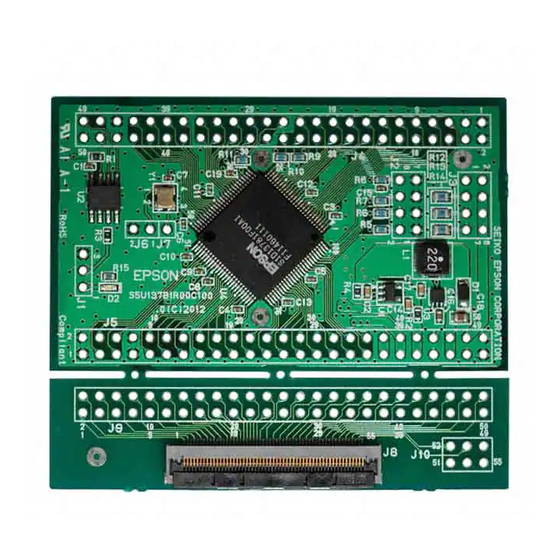
Page 10: Connectors
Figure 4-1 Reference Board Connector Locations J4 Host Interface Connector The host interface pins of S1D13781 are connected to J4 of the S5U13781R00C100 reference board. See Figure 7-1, S5U13781R00C100 Schematic Diagram (1 of 2), and Figure 7-2, S5U13781R00C100 Schematic Diagram (2 of 2), for detailed pin allocation. -
Page 11: J8 ~ J9 Connectors For Panel Connection
Page 11 J8 ~ J9 Connectors for Panel Connection J8 through J10 on the S5U13781R00C100 reference board are standard connectors used to implement suitable connection for various LCD panels. J8 is a 0.5mm pitch FPC connector (FH28-55S, bottom electrode type). See Figure 7-1, S5U13781R00C100 Schematic Diagram (1 of 2), and Figure 7-2, S5U13781R00C100 Schematic Diagram (2 of 2), for detailed pin allocation. -
Page 12: Others
Page 12 Others Quartz-Crystal Resonator for CLKI S5U13781R00C100 reference board includes Y1 (SG-310SCF 24MHz oscillator) for the CLKI input of the S1D13781. The output of the oscillator is disabled by connecting J6 1-2 and enabled by disconnecting. SPI flash memory The S5U13781R00C100 reference board includes SPI NOR FLASH standard memory of 16Mbit capacity. -
Page 13: Parts List
Page 13 Parts list Table 6-1 S5U13781R00C100 Bill of Materials Reference Size Part Description Manufac turer TQFP 14.0x14.0x1.7 S1D13781 LCD Controller EPSON 3225 3.2x2.5x1.2 SG-310SCF OSC 24MHz EPSON 2.1x2.1x0.8 TPS61161ADRVT LED Driver QFN2x2 SSOP5 3.1x3.0x1.25 BU15TD3WG Regulator LDO ROHM 5050 5.0x5.0x2.0... -
Page 14: Schematic Diagram
Page 14 Schematic Diagram Figure 7-1 S5U13781R00C100 Schematic Diagram (1 of 2) S5U13781R00C100 Reference Board User Manual X94A-G-004-01 Revision 1.0 Issue Date: 2012/03/26 Seiko Epson Corporation... - Page 15 Page 15 Figure 7-2 S5U13781R00C100 Schematic Diagram (2 of 2) X94A-G-004-01 S5U13781R00C100 Reference Board User Manual Issue Date: 2012/03/26 Revision 1.0 Seiko Epson Corporation...
-
Page 16: Board Layout And Dimensions
Page 16 Board Layout and Dimensions Figure 8-1 S5U13781R00C100 Board Layout Silk Screen S5U13781R00C100 Reference Board User Manual X94A-G-004-01 Revision 1.0 Issue Date: 2012/03/26 Seiko Epson Corporation... - Page 17 Page 17 Figure 8-2 S5U13781R00C100 Board Layout Top View Figure 8-3 S5U13781R00C100 Board Layout Bottom View X94A-G-004-01 S5U13781R00C100 Reference Board User Manual Issue Date: 2012/03/26 Revision 1.0 Seiko Epson Corporation...
- Page 18 Page 18 Figure 8-4 S5U13781R00C100 Board Dimensions (units: mm) S5U13781R00C100 Reference Board User Manual X94A-G-004-01 Revision 1.0 Issue Date: 2012/03/26 Seiko Epson Corporation...
-
Page 19: References
Page 19 References Epson Research and Development, Inc., S1D13781 Hardware Functional Specification, document number X94A-A-001-xx. X94A-G-004-01 S5U13781R00C100 Reference Board User Manual Issue Date: 2012/03/26 Revision 1.0 Seiko Epson Corporation... -
Page 20: 10 Change Record
Page 20 10 Change Record X94A-G-005-01 Revision 1.0 - Issued: March 26, 2012 Release document as rev 1.0 S5U13781R00C100 Reference Board User Manual X94A-G-004-01 Revision 1.0 Issue Date: 2012/03/26 Seiko Epson Corporation... - Page 21 EPSON HONG KONG LTD. Unit 715-723, 7/F Trade Square, 681 Cheung Sha Wan Road, Kowloon, Hong Kong. Phone: +852-2585-4600 FAX: +852-2827-4346 EPSON TAIWAN TECHNOLOGY & TRADING LTD. 14F, No. 7, Song Ren Road, Taipei 110, TAIWAN Phone: +886-2-8786-6688 FAX: +886-2-8786-6660 EPSON SINGAPORE PTE., LTD.
Need help?
Do you have a question about the S5U13781R00C100 and is the answer not in the manual?
Questions and answers