Table of Contents
Advertisement
Quick Links
S1D13706 Embedded Memory LCD Controller
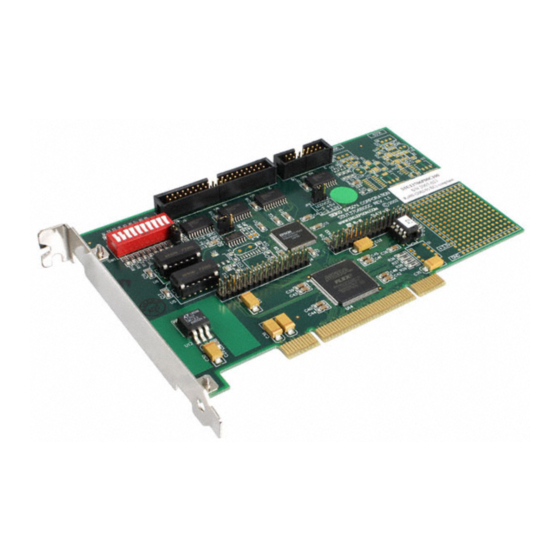
S5U13706P00C100 Evaluation Board
User Manual
Document Number: X31B-G-021-01
Status: Revision 1.1
Issue Date: 2009/03/03
© SEIKO EPSON CORPORATION 2007 - 2009. All Rights Reserved.
Information in this document is subject to change without notice. You may download and use this document, but only for your own use in
evaluating Seiko Epson/EPSON products. You may not modify the document. Epson Research and Development, Inc. disclaims any
representation that the contents of this document are accurate or current. The Programs/Technologies described in this document may contain
material protected under U.S. and/or International Patent laws.
EPSON is a registered trademark of Seiko Epson Corporation. All other Trademarks are the property of their respective owners
Revision 1.1
Advertisement
Table of Contents

Related Manuals for Epson S5U13700P00C000


Summary of Contents for Epson S5U13700P00C000
- Page 1 The Programs/Technologies described in this document may contain material protected under U.S. and/or International Patent laws. EPSON is a registered trademark of Seiko Epson Corporation. All other Trademarks are the property of their respective owners Revision 1.1...
- Page 2 Page 2 Epson Research and Development Vancouver Design Center S1D13706 S5U13706P00C100 Evaluation Board User Manual X31B-G-021-01 Issue Date: 2009/03/03 Revision 1.1...
-
Page 3: Table Of Contents
11 Technical Support ........28 11.1 EPSON LCD Controllers (S1D13706) ..... 28... - Page 4 Page 4 Epson Research and Development Vancouver Design Center S1D13706 S5U13706P00C100 Evaluation Board User Manual X31B-G-021-01 Issue Date: 2009/03/03 Revision 1.1...
-
Page 5: Introduction
Board. The board is designed as an evaluation platform for the S1D13706 Embedded Memory LCD Controller. This user manual is updated as appropriate. Please check the Epson Research and Devel- opment website at www.erd.epson.com for the latest revision of this document before beginning any development. -
Page 6: Features
• 4/8/16-bit 3.3V or 5V single color passive LCD panel support. • 9/12/18-bit 3.3V or 5V active matrix TFT LCD panel support. • Direct interface for 18-bit Epson D-TFD LCD panel support. • Direct interface for 18-bit Sharp HR-TFT LCD panel support. -
Page 7: Installation And Configuration
Epson Research and Development Page 7 Vancouver Design Center 3 Installation and Configuration The S5U13706P00C100 is designed to support as many platforms as possible. The S5U13706P00C100 incorporates a DIP switch and three jumpers which allow both the evaluation board and S1D13706 LCD controller to be configured for a specified evaluation platform. - Page 8 Page 8 Epson Research and Development Vancouver Design Center The S1D13706 has 8 configuration inputs (CNF[7:0]) which are read on the rising edge of RESET#. All S1D13706 configuration inputs are fully configurable using a ten position DIP switch as described below.
-
Page 9: Configuration Jumpers
HR-TFT and D-TFD panels as GPIO0 is required for both panels. For details, refer to the S1D13706 Hardware Functional Specification, document number X31B-A-001-xx. Note When configured for Sharp HR-TFT or Epson D-TFD panels, JP1 must be set to no jumper and JP6 must be set to position 2-3. GPIO0 connected GPIO0 disconnected... - Page 10 Position 1-2 sets the voltage level to 5.0V. Position 2-3 sets the voltage level to 3.3V (default setting). Note When configured for Sharp HR-TFT or Epson D-TFD panels, JP1 must be set to no jumper and JP6 must be set to position 2-3. 5.0V 3.3V...
-
Page 11: Cpu Interface
Epson Research and Development Page 11 Vancouver Design Center 4 CPU Interface 4.1 CPU Interface Pin Mapping Table 4-1: CPU Interface Pin Mapping Motorola S1D13706 Hitachi Motorola Motorola Motorola MC68EZ328/ Generic #1 Generic #2 Pin Name SH-3 /SH-4 MC68K #1... -
Page 12: Cpu Bus Connector Pin Mapping
Page 12 Epson Research and Development Vancouver Design Center CPU Bus Connector Pin Mapping Table 4-2: CPU Bus Connector (H3) Pinout Connector Comments Pin No. Connected to DB0 of the S1D13706 Connected to DB1 of the S1D13706 Connected to DB2 of the S1D13706... - Page 13 Epson Research and Development Page 13 Vancouver Design Center Table 4-3: CPU Bus Connector (H4) Pinout Connector Comments Pin No. Connected to A0 of the S1D13706 Connected to A1 of the S1D13706 Connected to A2 of the S1D13706 Connected to A3 of the S1D13706...
-
Page 14: Lcd Interface Pin Mapping
Page 14 Epson Research and Development Vancouver Design Center 5 LCD Interface Pin Mapping Table 5-1: LCD Signal Connector (H1) Monochrome Color Passive Panel Color TFT Panel Passive Connector Single Sharp Epson Name Pin No. Single Others HR-TFT D-TFD Format 1 Format 2... - Page 15 Epson Research and Development Page 15 Vancouver Design Center Table 5-2: Extended LCD Signal Connector (H2) Monochrome Color Passive Panel Color TFT Panel Passive Panel Connector Single Name Pin No. Single Others HR-TFT D-TFD Format 1 Format 2 4-bit 8-bit...
-
Page 16: Technical Description
Page 16 Epson Research and Development Vancouver Design Center 6 Technical Description 6.1 PCI Bus Support The S1D13706 does not have on-chip PCI bus interface support. The S1D13706P00C100 uses the PCI Bridge FPGA to support the PCI bus. 6.2 Direct Host Bus Interface Support The S5U13706P00C100 is specifically designed to work using the PCI Bridge FPGA in a standard PCI bus environment. -
Page 17: Passive/Active Lcd Panel Support
LCD Panel Voltage” on page 10 for information on setting the panel voltage). 6.5.2 Extended LCD Connector The S1D13706 directly supports Sharp 18-bit HR-TFT and Epson 18-bit D-TFD panels. The extended LCD connector (H2) provides the extra signals required to support these panels. -
Page 18: References
7 References 7.1 Documents • Epson Research and Development, Inc., S1D13706 Hardware Functional Specification, document number X31B-A-001-xx. • Epson Research and Development, Inc., S1D13706 Programming Notes and Examples, document number X31B-G-003-xx. 7.2 Document Sources • Epson Research and Development: http://www.erd.epson.com. -
Page 19: Parts List
Epson Research and Development Page 19 Vancouver Design Center 8 Parts List Table 8-1: Parts List Manufacturer / Part No. / Item Reference Part Description Assembly Instructions C1, C2, C3, C4, C5, C6, Panasonic-ECG ECJ- C7, C8, C9, C10, C11, 50V X7R +/-5%, 1206 3VB1H104K. - Page 20 Page 20 Epson Research and Development Vancouver Design Center Table 8-1: Parts List Manufacturer / Part No. / Item Reference Part Description Assembly Instructions N-channel FET, SOT-223 Do not purchase. Do not MMFT3055VL pckg. populate. High gain transistor, SOT- Do not purchase. Do not FZT792A 223 pckg.
- Page 21 Epson Research and Development Page 21 Vancouver Design Center Table 8-1: Parts List Manufacturer / Part No. / Item Reference Part Description Assembly Instructions 14 pin narrow DIP, screw U6, U5 Test Socket machine socket U7, U8, U9, U10 74HCT244...
-
Page 22: Schematics
Page 22 Epson Research and Development Vancouver Design Center 9 Schematics Figure 9-1: S5U13706P00C100 Schematics (1 of 5) S1D13706 S5U13706P00C100 Evaluation Board User Manual X31B-G-021-01 Issue Date: 2009/03/03 Revision 1.1... - Page 23 Epson Research and Development Page 23 Vancouver Design Center Figure 9-2: S5U13706P00C100 Schematics (2 of 5) S5U13706P00C100 Evaluation Board User Manual S1D13706 Issue Date: 2009/03/03 X31B-G-021-01 Revision 1.1...
- Page 24 Page 24 Epson Research and Development Vancouver Design Center Figure 9-3: S5U13706P00C100 Schematics (3 of 5) S1D13706 S5U13706P00C100 Evaluation Board User Manual X31B-G-021-01 Issue Date: 2009/03/03 Revision 1.1...
- Page 25 Epson Research and Development Page 25 Vancouver Design Center Figure 9-4: S5U13706P00C100 Schematics (4 of 5) S5U13706P00C100 Evaluation Board User Manual S1D13706 Issue Date: 2009/03/03 X31B-G-021-01 Revision 1.1...
- Page 26 Page 26 Epson Research and Development Vancouver Design Center Figure 9-5: S5U13706P00C100 Schematics (5 of 5) S1D13706 S5U13706P00C100 Evaluation Board User Manual X31B-G-021-01 Issue Date: 2009/03/03 Revision 1.1...
-
Page 27: Board Layout
Epson Research and Development Page 27 Vancouver Design Center 10 Board Layout Figure 10-1: S5U13706P00C100 Board Layout S5U13706P00C100 Evaluation Board User Manual S1D13706 Issue Date: 2009/03/03 X31B-G-021-01 Revision 1.1... -
Page 28: Technical Support
20/F, Harbour Centre, 25 Harbour Road Wanchai, Hong Kong Phone: +852-2585-4600 FAX: +852-2827-4346 Telex: 65542 EPSCO HX EPSON TAIWAN TECHNOLOGY & TRADING LTD. 14F, No. 7, Song Ren Road, Taipei 110, TAIWAN Phone: +886-2-8786-6688 FAX: +886-2-8786-6660 EPSON SINGAPORE PTE., LTD. - Page 29 Epson Research and Development Page 29 Vancouver Design Center Change Record X31B-G-021-01 Revision 1.1 - Issued: March 03, 2009 • section 11 - update sales office addresses X31B-G-021-01 Revision 1.0 - Issued: March 19, 2007 • initial draft • minor edits •...
Need help?
Do you have a question about the S5U13700P00C000 and is the answer not in the manual?
Questions and answers