Table of Contents
Advertisement
Advertisement
Table of Contents

Related Manuals for Motorola MVME162


Summary of Contents for Motorola MVME162
- Page 1 MVME162 Embedded Controller User’s Manual (MVME162/D2)
- Page 2 Motorola, Inc. assumes no liability resulting from any omissions in this document, or from the use of the information obtained therein. Motorola reserves the right to revise this document and to make changes from time to time in the content hereof without obligation of Motorola to notify any person of such revision or changes.
- Page 3 Preface The MVME162 User’s Manual provides general information, hardware preparation and installation instructions, operating instructions, and a functional description for the MVME162 Embedded Controller. This manual is intended for anyone who wants to design OEM systems, supply additional capability to an existing compatible system, or work in a lab environment for experimental purposes.
- Page 4 The computer programs stored in the Read Only Memory of this device contain material copyrighted by Motorola Inc., first published 1990, and may be used only under a license such as the License for Computer Programs (Article 14) contained in Motorola’s Terms and Conditions of Sale, Rev.
- Page 5 Inc. assumes no liability for the customer’s failure to comply with these requirements. The safety precautions listed below represent warnings of certain dangers of which Motorola is aware. You, as the user of the product, should follow these warnings and all other safety precautions necessary for the safe operation of the equipment in your operating environment.
-
Page 7: Table Of Contents
Contents CHAPTER 1 GENERAL INFORMATION Introduction ......................1-1 Models ........................1-1 Features........................1-2 Specifications ......................1-3 Cooling Requirements..................1-4 Special Considerations for Elevated Temperature Operation ....1-4 FCC Compliance ....................1-5 General Description ....................1-6 Input/Output ....................1-6 VMEbus Interface ....................1-7 No-VMEbus-Interface Option................1-7 MCchip ......................1-7 Flash Memory and EPROM................1-7 IndustryPack Modules ..................1-8 Optional SCSI Interface...................1-8 Optional LAN Ethernet Transceiver Interface ..........1-8... - Page 8 Clock Select Header (J12) for Serial Port 2 ............2-6 SRAM Battery Backup Source Select Header (J20) .........2-7 EPROM Size Select Header (J21) ...............2-7 General-Purpose Readable Jumpers Header (J22)..........2-8 Installation Instructions .....................2-9 IP Installation on the MVME162 ...............2-9 MVME162 Module Installation ...............2-10 System Considerations ..................2-12 CHAPTER 3 OPERATING INSTRUCTIONS Introduction .........................3-1...
- Page 9 CHAPTER 4 FUNCTIONAL DESCRIPTION Introduction ........................ 4-1 MVME162 Functional Description ................4-1 Data Bus Structure ....................4-1 MC68040/MC68LC040 MPU ................4-2 EPROM and Flash Memory................4-2 SRAM........................4-2 About the Battery..................4-3 Onboard DRAM ....................4-4 Battery Backed Up RAM and Clock..............4-5 VMEbus Interface and VMEchip2 ..............
- Page 11 Figure 2-2. Serial Interface Module, Connector Side .........2-4 Figure 2-3. MVME162/MVME712M EIA-232-D Connection Diagram ..2-14 Figure 2-4. MVME162/MVME712x EIA-232-D Connection Diagram ..2-20 Figure 2-5. MVME162 EIA-530 Connection Diagram........2-24 Figure 4-1. MVME162 Main Module Block Diagram ........4-13 Figure 4-2. Parity DRAM Mezzanine Module Block Diagram.......4-14...
- Page 13 List of Tables Table 1-1. MVME162 Models.................1-1 Table 1-2. MVME162 Specifications..............1-3 Table 2-1. Serial Interface Module Part Numbers..........2-4 Table 3-1. Local Bus Memory Map ...............3-4 Table 3-2. Local I/O Devices Memory Map ............3-5 Table 3-3. VMEchip2 Memory Map..............3-8 Table 3-4. MCchip Register Map .................3-14 Table 3-5.
-
Page 15: General Information
MVME162 Embedded Controller (referred to as the MVME162 throughout this manual). Models The MVME162 is available in several models, which are listed in Table 1-1. Table 1-1. MVME162 Models Model Description... -
Page 16: Features
General Information Features Features of the MVME162 include: 25MHz 32-bit Microprocessor: either an MC68LC040 Enhanced 32-bit Microprocessor with 8KB of cache and MMU, or an optional 25MHz MC68040 32-bit Microprocessor with 8KB of cache, MMU, and FPU 1MB, 4MB, or 8MB of shared Dynamic Random Access Memory (DRAM) -
Page 17: Specifications
, and FAIL STAT SCON FUSE SCSI Specifications Table 1-2, MVME162 Specifications, lists the specifications for an MVME162 without IndustryPacks. The subsequent sections detail cooling requirements and FCC compliance. Table 1-2. MVME162 Specifications Characteristics Specifications Power requirements +5V (± 5%), 3.5 A typical, 4.5 A maximum (with PROM;... -
Page 18: Cooling Requirements
The following information is for users whose applications for the MVME162 may subject it to high temperatures. The MVME162 uses commercial grade devices. Therefore, it can operate in an environment with ambient air temperatures from 0° C to 70° C. Several factors influence the ambient temperature seen by components on the MVME162. -
Page 19: Fcc Compliance
The following are some steps that the user can take to help make elevated- temperature operation possible: Position the MVME162 board in the chassis for maximum airflow over the component side of the board. Avoid placing boards with high power dissipation adjacent to the MVME162. -
Page 20: General Description
An I/O device may be connected to serial port 1 (or 2) on the MVME162 or to serial port 2 (or 4) on the MVME712, but not both. (That is, if an I/O device is connected to MVME162 port 1, no other I/O device should be connected to MVME712 port 2;... -
Page 21: Vmebus Interface
Flash Memory and EPROM The MVME162 is equipped with 1MB of Flash memory and an EPROM socket ready for the installation of the EPROM, which may be ordered separately. Flash memory is either a single device organized in a 1Mbit x 8 configuration or four devices organized in a 256Kbit x 8 configuration. -
Page 22: Industrypack Modules
Flash memory or from the EPROM. IndustryPack Modules Up to four IndustryPack (IP) modules may be installed on the MVME162. The interface between the IPs and MVME162 is the IndustryPack Interface Controller (IPIC) ASIC. Access to the IPs is provided by four 3M connectors located behind the MVME162 front panel. -
Page 23: Mvme712 Series Transition Modules
An I/O device may be connected to serial port 1 (or 2) on the MVME162 or to serial port 2 (or 4) on the MVME712, but not to both ports. (That is, if an I/O device is connected to MVME162 port 1, no other I/O device should be connected to MVME712 port 2;... -
Page 24: Related Documentation
General Information Related Documentation The following publications are applicable to the MVME162 and may provide additional helpful information. If not shipped with this product, they may be purchased by contacting your local Motorola sales office. Non-Motorola documents may be purchased from the sources listed. -
Page 25: Support Information
28F020 Flash Memory Data Sheet, Order Number 290245-003; Intel Literature Sales, P.O. Box 7641, Mt. Prospect, IL 60056-7641. Support Information You can obtain connector interconnect signal information, parts lists, and schematics for the MVME162 free of charge by contacting your local Motorola sales office. MVME162/D2 1-11... -
Page 26: Manual Terminology
A byte is eight bits, numbered 0 through 7, with bit 0 being the least significant. A word is 16 bits, numbered 0 through 15, with bit 0 being the least significant. A longword is 32 bits, numbered 0 through 31, with bit 0 being the least significant. 1-12 MVME162 Embedded Controller User’s Manual... -
Page 27: Hardware Preparation And Installation
The MVME162 provides software control over most options: by setting bits in control registers after installing the MVME162 in a system, you can modify its configuration. (The MVME162 registers are described in Chapter 4, and/or in the MVME162 Embedded Controller Programmer’s Reference Guide as listed in Related Documentation in Chapter 1.) -
Page 28: Sim Selection
SERIAL PORT 2 For the location of SIM connector J10 on the MVME162, refer to Figure 2-1. Figure 2-2 illustrates the secondary side (bottom) of a serial interface module, showing the J1 connector which plugs into SIM connector J10 on the MVME162. -
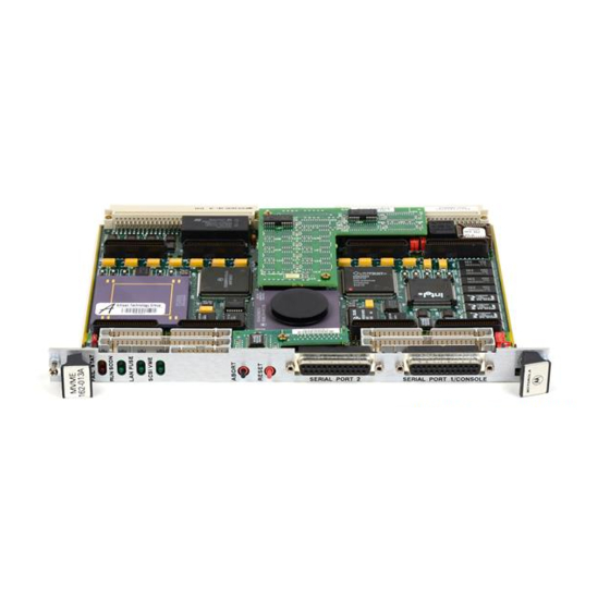
Page 29: Figure 2-1. Mvme162 Switch, Header, Connector, Fuse, And Led Locations
Hardware Preparation MVME 162-XX FAIL STAT RUN SCON FUSE SCSI VME ABORT RESET Figure 2-1. MVME162 Switch, Header, Connector, Fuse, and LED Locations MVME162/D2... -
Page 30: Removal Of Existing Sim
Grasp opposite sides of the SIM and gently lift straight up. Avoid lifting the SIM by one side only, as the connector can aution be damaged on the SIM or the main board. Place the SIM in a static-safe container for possible reuse. MVME162 Embedded Controller User’s Manual... -
Page 31: Installation Of New Sim
Installation of New SIM Observe the orientation of the connector keys on SIM connector J1 and MVME162 connector J10. Turn the SIM so that the keys line up and place it gently on connector J10, aligning the mounting holes at the SIM corners with the matching standoffs on the MVME162. -
Page 32: Synchronous Clock Select Header (J11) For Serial Port 1/Console
Hardware Preparation and Installation Synchronous Clock Select Header (J11) for Serial Port 1/Console The MVME162 is shipped from the factory with the SERIAL PORT 1/CONSOLE header configured for asynchronous communications (i.e., jumpers removed). To select synchronous communications for the SERIAL PORT 1/CONSOLE connection, install jumpers across pins 1 and 2 and pins 3 and 4. -
Page 33: Sram Battery Backup Source Select Header (J20)
Hardware Preparation SRAM Battery Backup Source Select Header (J20) The MVME162 is factory-configured to use VMEbus +5V standby power as a backup power source for the SRAM (i.e., jumpers are installed across pins 1 and 3 and 2 and 4). To select the onboard battery as the backup power source, install the jumpers across pins 3 and 5 and 4 and 6. -
Page 34: General-Purpose Readable Jumpers Header (J22)
Pins 9-10 (GPIO3) are reserved to select either the Flash memory map (jumper installed) or the EPROM memory map (jumper removed). They are not user-definable. The MVME162 is shipped from the factory with J22 set to all zeros (jumpers on all pins). 162BUG INSTALLED... -
Page 35: Installation Instructions
Because of the varying requirements for each different kind of IP, Motorola does not supply these cables. – Bring the IP cables out the narrow slots in the MVME162 front panel and attach them to the appropriate external equipment, depending on the nature of the particular IP(s). -
Page 36: Mvme162 Module Installation
IACK daisy-chain driver. – If you do not intend to use the MVME162 as system controller, it can occupy any unused double-height card slot. Slide the MVME162 into the selected card slot. Be sure the module is seated properly in the P1 and P2 connectors on the backplane. - Page 37 Related Documentation in Chapter 1 (the MVME162 Embedded Controller Programmer’s Reference Guide provides some connection diagrams). If you intend to use the MVME162 with Port B in an EIA-530 configuration, do not install the P2 or LCP2 Adapter Board and the MVME712 series transition module. They are in- compatible with the EIA-530 interface (refer to MVME162 Serial Port 2 in Chapter 4, Functional Description).
-
Page 38: System Considerations
VMEbus backplane connectors P1 and P2. Whether the MVME162 operates as a VMEbus master or as a VMEbus slave, it is configured for 32 bits of address and 32 bits of data (A32/D32). However, it handles A16 or A24 devices in the address ranges indicated in Chapter 3. - Page 39 If the Ethernet transceiver fails to operate, check fuse F2. The MVME162 provides SCSI terminator power through a 1A fuse (F1) located on the P2 Adapter Board or LCP2 Adapter Board. If the fuse is blown, the SCSI device(s) may function erratically or not at all.
-
Page 40: Figure 2-3. Mvme162/Mvme712M Eia-232-D Connection Diagram
PIN 20 PIN 8 MVME162 EIA-232-D DCE CONFIGURATION PIN 6 (TO TERMINAL) PIN 15 PIN 17 TXCO PIN 24 PIN 7 10970.00 (1-6) 9405 Figure 2-3. MVME162/MVME712M EIA-232-D Connection Diagram (Sheet 1 of 6) 2-14 MVME162 Embedded Controller User’s Manual... - Page 41 PIN 4 PIN 5 PIN 20 PIN 8 MVME162 EIA-232-D DCE CONFIGURATION PIN 6 (TO TERMINAL) PIN 15 PIN 17 TXCO PIN 24 PIN 7 10970.00 (2-6) 9405 Figure 2-3. MVME162/MVME712M EIA-232-D Connection Diagram (Sheet 2 of 6) MVME162/D2 2-15...
- Page 42 PIN 20 PIN 8 MVME 162 EIA-232-D DTE CONFIGURATION PIN 6 (TO MODEM) PIN 15 PIN 17 TXCO PIN 24 PIN 7 10970.00 (3-6) 9405 Figure 2-3. MVME162/MVME712M EIA-232-D Connection Diagram (Sheet 3 of 6) 2-16 MVME162 Embedded Controller User’s Manual...
- Page 43 PIN 4 PIN 5 PIN 20 PIN 8 MVME 162 EIA-232-D DCE CONFIGURATION PIN 6 (TO TERMINAL) PIN 15 PIN 17 TXCO PIN 24 PIN 7 10970.00 (4-6) 9405 Figure 2-3. MVME162/MVME712M EIA-232-D Connection Diagram (Sheet 4 of 6) MVME162/D2 2-17...
- Page 44 PIN 20 PIN 8 MVME 162 EIA-232-D DTE CONFIGURATION PIN 6 (TO MODEM) PIN 15 PIN 17 TXCO PIN 24 PIN 7 10970.00 (5-6) 9405 Figure 2-3. MVME162/MVME712M EIA-232-D Connection Diagram (Sheet 5 of 6) 2-18 MVME162 Embedded Controller User’s Manual...
- Page 45 PIN 4 PIN 5 PIN 20 PIN 8 MVME 162 EIA-232-D DCE CONFIGURATION PIN 6 (TO TERMINAL) PIN 15 PIN 17 TXCO PIN 24 PIN 7 10970.00 (6-6) 9405 Figure 2-3. MVME162/MVME712M EIA-232-D Connection Diagram (Sheet 6 of 6) MVME162/D2 2-19...
-
Page 46: Figure 2-4. Mvme162/Mvme712X Eia-232-D Connection Diagram
PIN 20 PIN 8 MVME162 RS232 DCE CONFIGURATION PIN 6 (TO TERMINAL) PIN 15 PIN 17 TXCO PIN 24 PIN 7 11020.00 9406 (1-4) Figure 2-4. MVME162/MVME712 x EIA-232-D Connection Diagram (Sheet 1 of 4) 2-20 MVME162 Embedded Controller User’s Manual... - Page 47 PIN 4 PIN 5 PIN 20 PIN 8 MVME162 RS232 DCE CONFIGURATION PIN 6 (TO TERMINAL) PIN 15 PIN 17 TXCO PIN 24 PIN 7 11020.00 9406 (2-4) Figure 2-4. MVME162/MVME712 x EIA-232-D Connection Diagram (Sheet 2 of 4) MVME162/D2 2-21...
- Page 48 PIN 8 MVME 162 RS232 DTE CONFIGURATION PIN 6 (TO MODEM) PIN 15 PIN 17 TXCO PIN 24 PIN 7 11020.00 9406 (3-4) Figure 2-4. MVME162/MVME712 x EIA-232-D Connection Diagram (Sheet 3 of 4) 2-22 MVME162 Embedded Controller User’s Manual...
- Page 49 PIN 5 PIN 20 PIN 8 MVME 162 RS232 DCE CONFIGURATION PIN 6 (TO TERMINAL) PIN 15 PIN 17 TXCO PIN 24 PIN 7 11020.00 9406 (4-4) Figure 2-4. MVME162/MVME712 x EIA-232-D Connection Diagram (Sheet 4 of 4) MVME162/D2 2-23...
-
Page 50: Figure 2-5. Mvme162 Eia-530 Connection Diagram
PIN 19 RL_A PIN 21 PIN 7 PIN 7 NOTE: SUFFIX _A = THE + SIGNAL. SUFFIX _B = THE - SIGNAL. 10971.00 (1-2) 9405 Figure 2-5. MVME162 EIA-530 Connection Diagram (Sheet 1 of 2) 2-24 MVME162 Embedded Controller User’s Manual... - Page 51 TM_A PIN 25 LL_A PIN 19 RL_A PIN 21 PIN 7 PIN 7 NOTE: SUFFIX _A = THE + SIGNAL. SUFFIX_-B = THE - SIGNAL. 10971.00 (2-2) 9405 Figure 2-5. MVME162 EIA-530 Connection Diagram (Sheet 2 of 2) MVME162/D2 2-25...
- Page 52 Hardware Preparation and Installation 2-26 MVME162 Embedded Controller User’s Manual...
-
Page 53: Operating Instructions
OPERATING INSTRUCTIONS Introduction This chapter provides information necessary to use the MVME162 in a system configuration. This includes a description of the switches and LEDs, memory maps, and software initialization of the module. Switches and LEDs The MVME162 front panel has... -
Page 54: Front Panel Indicators (Ds1 - Ds4)
LED (red). Lights when the BRDFAIL* signal line is active. Part of FAIL DS1. LED (yellow). Driven by the MC68040 status lines on the MVME162. STAT Lights when a halt condition from the processor is detected. Part of DS1. LED (green). Lights when the local bus TIP* signal line is low. This indicates one of the local bus masters is executing a local bus cycle. -
Page 55: Memory Maps
The normal address range is defined by the TT signals on the local bus. For the MVME162, transfer types 0, 1, and 2 define the normal address range. Table 3-1 defines the entire map ($00000000 to $FFFFFFFF). -
Page 56: Table 3-1. Local Bus Memory Map
Operating Instructions Table 3-1. Local Bus Memory Map Software Address Range Devices Accessed Port Width Size Cache Notes Inhibit Programmable DRAM on Board 1MB-8MB Programmable 128KB-2MB SRAM Programmable VMEbus A32/A24 D32/D16 Programmable IP_a Memory D32-D8 64 KB-8 MB 2, 4 Programmable IP_b Memory D32-D8... -
Page 57: Table 3-2. Local I/O Devices Memory Map
$FFF58000 - $FFF5807F IPIC IP_a I/O 128 B $FFF58080 - $FFF580FF IPIC IP_a ID 128 B $FFF58100 - $FFF5817F IPIC IP_b I/O 128 B $FFF58180 - $FFF581FF IPIC IP_b ID Read 128 B $FFF58200 - $FFF5827F IPIC IP_c I/O 128 B MVME162/D2... - Page 58 Operating Instructions Table 3-2. Local I/O Devices Memory Map (Continued) Address Range Devices Accessed Port Width Size Notes $FFF58280 - $FFF582FF IPIC IP_c ID 128 B $FFF58300 - $FFF5837F IPIC IP_d I/O 128 B $FFF58380 - $FFF583FF IPIC IP_d ID Read 128 B $FFF58400 - $FFF584FF IPIC IP_ab I/O...
-
Page 59: Detailed I/O Memory Maps
Detailed I/O Memory Maps Tables 3-3 through 3-12 provide detailed memory maps for the VMEchip2, the MCchip, the Zilog Z85230 serial communications controller, the Intel 82596CA LAN controller, the NCR 53C710 SCSI controller, the IPIC chip, and the MK48T08 BBRAM/TOD Clock. MVME162/D2... -
Page 60: Table 3-3. Vmechip2 Memory Map
Operating Instructions Table 3-3. VMEchip2 Memory Map (Sheet 1 of 3) VMEchip2 LCSR Base Address = $FFF40000 OFFSET: SLAVE ENDING ADDRESS 1 SLAVE ENDING ADDRESS 2 SLAVE ADDRESS TRANSLATION ADDRESS 1 SLAVE ADDRESS TRANSLATION ADDRESS 2 ADDER PRGM DATA MASTER ENDING ADDRESS 1 MASTER ENDING ADDRESS 2 MASTER ENDING ADDRESS 3 MASTER ENDING ADDRESS 4... - Page 61 MAST MASTER ROBN FAIR VMEBUS HALT FAIR RELM VMEBUS DMA LB SNP MODE LOCAL BUS ADDRESS COUNTER VMEBUS ADDRESS COUNTER BYTE COUNTER TABLE ADDRESS COUNTER DMA TABLE DONE INTERRUPT COUNT STAT 1360 9403 This sheet begins on facing page. MVME162/D2...
- Page 62 Operating Instructions Table 3-3. VMEchip2 Memory Map (Sheet 2 of 3) VMEchip2 LCSR Base Address = $FFF40000 OFFSET: BGTO GLOBAL TIME OFF TIME ON TIMER TICK TIMER 1 TICK TIMER 1 TICK TIMER 2 TICK TIMER 2 SCON PURS FAIL FAIL STAT PURS...
- Page 63 IRQ LEVEL IRQ LEVEL VME IRQ 4 VMEB IRQ 3 VME IRQ 2 VME IRQ 1 IRQ LEVEL IRQ LEVEL IRQ LEVEL IRQ LEVEL GPIOO GPIOI EROM SRAM BSYT BBSY 1361 9403 This sheet begins on facing page. MVME162/D2 3-11...
- Page 64 Operating Instructions This page intentionally left blank. 3-12 User’s Manual...
- Page 65 GENERAL PURPOSE CONTROL AND STATUS REGISTER 0 GENERAL PURPOSE CONTROL AND STATUS REGISTER 1 GENERAL PURPOSE CONTROL AND STATUS REGISTER 2 GENERAL PURPOSE CONTROL AND STATUS REGISTER 3 GENERAL PURPOSE CONTROL AND STATUS REGISTER 4 GENERAL PURPOSE CONTROL AND STATUS REGISTER 5 MVME162/D2 3-13...
-
Page 66: Table 3-4. Mcchip Register Map
LANC Error (Reserved) LANC Interrupt LANC Bus Error Status Control Interrupt Control SCSI Error Status General Purpose MVME162 SCSI Interrupt Inputs Version Control Tick Timer 3 Compare Register Tick Timer 3 Counter Register Tick Timer 4 Compare Register Tick Timer 4 Counter Register... -
Page 67: Table 3-5. Z85230 Scc Register Addresses
MPU Channel Attention (CA) 1. Refer to the MPU Port and MPU Channel Attention registers otes in the MVME162 Embedded Controller Programmer’s Reference Guide. 2. After resetting, you must write the System Configuration Pointer to the command registers before writing to the MPU Channel Attention register. -
Page 68: Table 3-7. 53C710 Scsi Memory Map
Operating Instructions Table 3-7. 53C710 SCSI Memory Map 53C710 Register Address Map Base Address is $FFF47000 SCRIPTs and Big Endian Little Endian Mode Mode SIEN SDID SCNTL1 SCNTL0 SOCL SODL SXFER SCID SBCL SBDL SIDL SFBR SSTAT2 SSTAT1 SSTAT0 DSTAT CTEST3 CTEST2 CTEST1... -
Page 69: Ipic Overall Memory Map
64 B $FFF58400-$FFF584FF IP_ab I/O Space D32-D16 256 B $FFF58500-$FFF585FF IP_cd I/O Space D32-D16 256 B $FFF58600-$FFF586FF IP_ab I/O Space Repeated D32-D16 256 B $FFF58700-$FFF587FF IP_cd I/O Space Repeated D32-D16 256 B $FFFBC000-$FFFBC01F Control/Status Registers D32-D8 32 B MVME162/D2 3-17... -
Page 70: Table 3-9. Ipic Memory Map-Control And Status Registers
Operating Instructions Table 3-9 contains a summary of the IPIC CSR registers. The CSR registers can be accessed as bytes, words, or longwords; they should not be accessed as lines. They are shown in the table as bytes. Table 3-9. IPIC Memory Map—Control and Status Registers IPIC Base Address = $FFFBC000 Register Bit Names Register... -
Page 71: Table 3-10. Mk48T08 Bbram/Tod Clock Memory Map
$FFFC1EFC - $FFFC1F07 Serial Number $FFFC1F08 - $FFFC1F17 Board ID $FFFC1F18 - $FFFC1F27 $FFFC1F28 - $FFFC1F2B Speed $FFFC1F2C - $FFFC1F31 Ethernet Address $FFFC1F32 - $FFFC1F33 Reserved $FFFC1F34 - $FFFC1F35 Local SCSI ID $FFFC1F36 - $FFFC1F3D Memory Mezzanine PWB MVME162/D2 3-19... -
Page 72: Table 3-12. Tod Clock Memory Map
Operating Instructions Table 3-11. BBRAM Configuration Area Memory Map (Continued) Address Range Description Size (Bytes) $FFFC1F3E - $FFFC1F45 Memory Mezzanine Serial Number $FFFC1F46 - $FFFC1F4D Serial Port 2 Personality PWB $FFFC1F4E - $FFFC1F55 Serial Port 2 Personality Serial No. $FFFC1F56 - $FFFC1F5D IP_a Board ID $FFFC1F5E - $FFFC1F65 IP_a Board Serial Number... -
Page 73: Bbram, Tod Clock Memory Map
(TOD) clock, is defined by the chip hardware. The first area is reserved for user data. The second area is used by Motorola networking software. The third area is used by the operating system. The fourth area is used by the MVME162 board debugger (MVME162Bug). - Page 74 For example, this field could contain: 000000470476 Sixteen bytes are reserved for the board ID in ASCII format. For example, for an MVME162 board with MC68040, SCSI, Ethernet, 4MB DRAM, and 512KB SRAM, this field contains: (The 10 characters are followed by six blanks.)
- Page 75 26. The final one byte of the area is reserved for a checksum (as defined in the MVME162Bug Debugging Package User’s Manual) for security and data integrity of the configuration area of the NVRAM. This data is stored in hexadecimal format. MVME162/D2 3-23...
-
Page 76: Interrupt Acknowledge Map
Software Initialization Most functions that have been done with switches or jumpers on other modules are done by setting control registers on the MVME162. At powerup or reset, the EPROMs that contain the 162Bug debugging package set up the default values of many of these registers. -
Page 77: Local Reset Operation
Any VMEbus access to the MVME162 while it is in the reset state is ignored. If a global bus timer is enabled, a bus error is generated. - Page 78 Operating Instructions 3-26 User’s Manual...
-
Page 79: Functional Description
Ethernet transceiver interface, and a non-VMEbus version. Data Bus Structure The local data bus on the MVME162 is a 32-bit synchronous bus that is based on the MC68040 bus, and which supports burst transfers and snooping. The various local bus master and slave devices use the local bus to communicate. -
Page 80: Mc68040/Mc68Lc040 Mpu
MCchip Programming Model in the MVME162 Embedded Controller Programmer’s Reference Guide. The SRAM arrays are not parity protected. The battery backup function for the MVME162 SRAM is provided by a Dallas DS1210S device that supports primary and secondary power sources. In the event of a main board power failure, the DS1210S checks power sources and switches to the source with the higher voltage. -
Page 81: About The Battery
The lifetime of the battery is very dependent on the ambient temperature of the board and the power-on duty cycle. The lithium battery supplied on the MVME162 should provide at least two years of backup time with the board powered off and with an ambient temperature of 40° C. If the power-on duty cycle is 50% (the board is powered on half of the time), the battery lifetime is four years. -
Page 82: Onboard Dram
Onboard DRAM The MVME162 offers a 1MB, a 4MB, and an 8MB DRAM option. The DRAM architecture is non-interleaved for 1MB and interleaved for 4MB and 8MB. Parity protection can be enabled with interrupts or bus exception when a parity error is detected. -
Page 83: Battery Backed Up Ram And Clock
MVME162 Functional Description Battery Backed Up RAM and Clock An MK48T08 RAM and clock chip is used on the MVME162. This chip provides a time-of-day clock, oscillator, crystal, power fail detection, memory write protection, 8KB of RAM, and a battery in one 28-pin package. The clock provides seconds, minutes, hours, day, date, month, and year in BCD 24-hour format. - Page 84 Although both ports are connected to the same Z85230 Port A, there are several differences between them: On the MVME162 front panel, Port 1 can be connected to the TxC and RxC clock signals which may be present on the DB25 connector. These connections are made via header J11 on the MVME162 board (see Figures 2-3 and 2-4 in Chapter 2).
- Page 85 Although both ports are connected to the same Z85230 Port B, there are several considerations to keep in mind: On the MVME162 front panel, Port 2 can be connected to the TxC and RxC clock signals which may be present on the DB25 connector. These connections are made via header J12 on the MVME162 board (see Figures 2-3, 2-4, and 2-5 in Chapter 2).
-
Page 86: Industrypack (Ip) Interfaces
Refer to the IPIC Programming Model in the MVME162 Embedded Controller Programmer’s Reference Guide for details of the IP interface. Refer to the MVME162 Embedded Controller Support Information manual for the pin assignments of the IP connectors. -
Page 87: Scsi Interface
The individual configuring the system must ensure that the SCSI bus is properly terminated at both ends. The MVME162 provides sockets for SCSI bus terminators on the P2 adapter board or the LCP2 adapter board. If the SCSI bus ends at the adapter board, then termination resistors must be installed on the adapter board. -
Page 88: Programmable Tick Timers
Programmer’s Reference Guide for detailed programming information. Local Bus Timeout The MVME162 provides timeout functions in the VMEchip2 and the MCchip for the local bus. When the timer is enabled and a local bus access times out, a Transfer Error Acknowledge (TEA) signal is sent to the local bus master. The timeout value is selectable by software for 8 µsec, 64 µsec, 256 µsec, or infinity. -
Page 89: Local Bus To Dram Cycle Times
The EPROM/Flash cycle time is programmable from 3 to 10 bus clocks/byte (4 bytes = 12 to 40). (The actual cycle time may vary depending on the device speed.) The data transfers are 32 bits wide. Refer to the MVME162 Embedded Controller Programmer’s Reference Guide. -
Page 90: Lan Dma Transfers
SCSI bus. LAN DMA Transfers The MVME162 includes a LAN interface with DMA controller. The LAN DMA controller uses a FIFO buffer to interface the serial LAN bus to the 32-bit local bus. The FIFO buffer allows the LAN DMA controller to efficiently transfer data to the local bus. - Page 91 MVME162 Functional Description MVME162/D2 4-13...
-
Page 92: Figure 4-1. Mvme162 Main Module Block Diagram
Functional Description Figure 4-1. MVME162 Main Module Block Diagram 4-14 User’s Manual... - Page 93 MVME162 Functional Description MVME162/D2 4-15...
-
Page 94: Figure 4-2. Parity Dram Mezzanine Module Block Diagram
Functional Description Figure 4-2. Parity DRAM Mezzanine Module Block Diagram 4-16 User’s Manual... -
Page 95: Introduction
SERIAL INTERCONNECTIONS Introduction As described in previous chapters of this manual, one of the MVME162’s two serial ports (port A internally, on the front panel) is SERIAL PORT 1/CONSOLE an EIA-232-D DCE port exclusively. The second port (port B internally,... -
Page 96: Table A-1. Eia-232-D Interconnections
Serial Interconnections Table A-1. EIA-232-D Interconnections Signal Signal Name and Description Number Mnemonic Not used. Transmit Data. Data to be transmitted; input to modem from terminal. Receive Data. Data which is demodulated from the receive line; output from modem to terminal. Request To Send. -
Page 97: Interface Characteristics
The EIA-232-D interface standard specifies all parameters for serial binary data interchange between DTE and DCE devices using unbalanced lines. EIA- 232-D transmitter and receiver parameters applicable to the MVME162 are listed in Tables A-2 and A-3. Table A-2. EIA-232-D Interface Transmitter Characteristics... -
Page 98: Eia-530 Connections
< +15V) 3000 7000 The MVME162 conforms to EIA-232-D specifications. Note that although the EIA-232-D standard recommends the use of short interconnection cables not more than 50 feet (15m) in length, longer cables are permissible provided the total load capacitance measured at the interface point and including signal terminator does not exceed 2500pF. - Page 99 Remote Loopback (A). Reroutes signal within remote DCE. In DTE configuration, always tied inactive and driven false. In DCE configuration, ignored. DSR_B Data Set Ready (B). Input to DTE from DCE to indicate that the DCE is ready to send or receive data. In DCE configuration, always true. MVME162/D2...
-
Page 100: Interface Characteristics
Inversion of signals may be required (e.g., plus polarity MARK to minus polarity MARK may be achieved by inverting the cable pair). EIA-530 interface transmitter and receiver parameters applicable to the MVME162 are listed in Tables A-5 and A-6. User’s Manual... -
Page 101: Table A-5. Eia-530 Interface Transmitter Characteristics
Table A-6. EIA-530 Interface Receiver Characteristics Value Parameter Unit Minimum Maximum ±12 Differential input voltage ±12 Input offset voltage Differential input high threshold voltage Differential input low threshold voltage -200 Differential input hysteresis Input impedance (without termination resistors) KΩ MVME162/D2... -
Page 102: Proper Grounding
Serial Interconnections Proper Grounding An important subject to consider is the use of ground pins. There are two pins labeled GND. Pin 7 is the signal ground and must be connected to the distant device to complete the circuit. Pin 1 is the chassis ground, but it must be used with care. - Page 103 Index When using this index, keep in mind that a page number indicates only where referenced material begins. It may extend to the page or pages following the page referenced. Numerics 162Bug package 1-8 EIA-232-D interconnections A-1 SIM part numbers 2-4 backplane jumpers 2-10 EIA-530 battery...
- Page 104 Index memory maps 3-3 53C710 SCSI 3-16 GCSR board control register 3-25 82596CA Ethernet LAN 3-15 general-purpose readable jumpers (J11) BBRAM configuration area 3-19 IPIC control/status 3-18 global bus timeout 2-12 IPIC overall 3-17 local bus 3-4 hardware interrupts 4-10 local I/O devices 3-5 hardware preparation 2-1 MCchip registers 3-14...
- Page 105 SCSI VMEbus FIFO buffer 4-11 address/data configurations 2-12 interface 1-2, 1-8, 4-9 interface 1-2, 1-7, 4-5 termination 4-9 system controller functions 4-5 terminator power 2-13 VMEchip2 1-7 serial communications interface 4-5 serial interface modules (SIMs) 2-2 watchdog timers 4-10 part numbers 2-4 port B configuration 4-6 selection 2-2 serial interface parameters A-3...
- Page 106 Index IN-4 User’s Manual...
Need help?
Do you have a question about the MVME162 and is the answer not in the manual?
Questions and answers