Table of Contents
Advertisement
Quick Links
The attached pages are updates to the MVME162 Embedded Controller Installation Guide.
They supply information reflecting recent changes made in the board layout, and
correct errors detected in the existing document since its release.
Please place this page behind the title page of the manual as a record of this change.
Replace pages according to the following table:
Preface through Safety Summary pages
vii/viii, ix/x, xiii/xiv
1-1/1-2 through 1-25/1-26
2-1/2-2 through 2-9/2-10
3-1/3-2 through 3-21/3-22
A-3/A-4, A-11/A-12
A vertical bar ( ) in the margin of a revised page indicates a text change or addition.
The supplement number appears at the bottom of each odd-numbered revised
page.
Supplement to
MVME162 Embedded Controller
Installation Guide
(MVME162IG/D2)
Replace Old
With New
Preface page through CE Mark page
vii/viii, ix/x, xiii/xiv
1-1/1-2 through 1-25/1-26
2-1/2-2 through 2-9/2-10
3-1/3-2 through 3-23/3-24
A-3/A-4, A-11/A-12
MVME162IG/D2A1
August 1996
Advertisement
Table of Contents

Related Manuals for Motorola MVME162


Summary of Contents for Motorola MVME162
- Page 1 MVME162 Embedded Controller Installation Guide (MVME162IG/D2) The attached pages are updates to the MVME162 Embedded Controller Installation Guide. They supply information reflecting recent changes made in the board layout, and correct errors detected in the existing document since its release.
-
Page 2: Restricted Rights Legend
Motorola, Inc. assumes no liability resulting from any omissions in this document, or from the use of the information obtained therein. Motorola reserves the right to revise this document and to make changes from time to time in the content hereof without obligation of Motorola to notify any person of such revision or changes. - Page 3 This manual provides a general board level hardware description, hardware preparation and installation instructions, debugger general information, and instructions for using the debugger in the MVME162 Embedded Controller. The information contained in this manual applies to the following MVME162 models:...
- Page 4 The computer programs stored in the Read Only Memory of this device contain material copyrighted by Motorola Inc., first published 1990, and may be used only under a license such as the License for Computer Programs (Article 14) contained in Motorola’s Terms and Conditions of Sale, Rev.
- Page 5 Inc. assumes no liability for the customer’s failure to comply with these requirements. The safety precautions listed below represent warnings of certain dangers of which Motorola is aware. You, as the user of the product, should follow these warnings and all other safety precautions necessary for the safe operation of the equipment in your operating environment.
- Page 6 All Motorola PWBs (printed wiring boards) are manufactured by UL-recognized manufacturers, with a flammability rating of 94V-0. This equipment generates, uses, and can radiate electro- magnetic energy. It may cause or be susceptible to electro- magnetic interference (EMI) if not installed and used in a WARNING cabinet with adequate EMI protection.
-
Page 7: Board Level Hardware Description
SCSI bus interface with DMA, VMEbus controller, and 512KB of SRAM with battery backup. The I/O on the MVME162 is connected to the VMEbus P2 connector. The main board is connected through a P2 transition board and cables to the transition boards. -
Page 8: Related Documentation
IPs that can be plugged into the MVME162 main module. Related Documentation The MVME162 does not ship with all of the documentation that is available for the product. The MVME162 instead ships with a start-up installation guide (the document you are presently reading) that includes all the information... - Page 9 Also available, but not included in the set, are MVME162IG/D and SIMVME162/D. To further assist your development effort, Motorola has collected user’s manuals for each of the peripheral controllers used on the MVME162 and other boards from the suppliers. This bundle includes manuals and data sheets, including the following:...
- Page 10 Board Level Hardware Description 68-1X7DS for use with the MVME162 and 167. NCR 53C710 SCSI Controller Data Manual and Programmer’s Guide Intel i82596 Ethernet Controller User’s Manual Cirrus Logic CD2401 Serial Controller User’s Manual SGS-Thompson MK48T08 NVRAM/TOD Clock Data Sheet The following publications are also available from the sources indicated.
- Page 11 Four 32-bit Tick Timers (in the MCchip ASIC) for periodic interrupts Two 32-bit Tick Timers (in the VMEchip2 ASIC) for periodic interrupts Watchdog timer Eight software interrupts (for MVME162 versions that have the VMEchip2) – Two serial ports (one EIA-232-D DCE; one EIA-232-D or EIA-530 DCE/DTE) –...
-
Page 12: Specifications
, and FAIL STAT SCON FUSE SCSI Specifications General specifications for the MVME162 are listed in Table 1-1. Table 1-1. MVME162 Specifications Characteristics Specifications Power requirements +5V (± 5%), 3.5 A typical, 4.5 A max. (with EPROM; without IPs) +12 Vdc (± 5%), 100 mA (max.) -12 Vdc (±... -
Page 13: Special Considerations For Elevated Temperature Operation
The following information is for users whose applications for the MVME162 may subject it to high temperatures. The MVME162 uses commercial grade devices. Therefore, it can operate in an environment with ambient air temperature from 0° C to 70° C. There are many factors that affect the ambient temperature seen by components on the MVME162: inlet air temperature;... -
Page 14: Manual Terminology
A byte is eight bits, numbered 0 through 7, with bit 0 being the least significant. A two-byte is 16 bits, numbered 0 through 15, with bit 0 being the least significant. For the MVME162 and other CISC modules, this is called a word. MVME162 Embedded Controller Installation Guide... -
Page 15: Block Diagram
Block Diagram A four-byte is 32 bits, numbered 0 through 31, with bit 0 being the least significant. For the MVME162 and other CISC modules, this is called a longword. The terms control bit and status bit are used extensively in this document. The term control bit is used to describe a bit in a register that can be set and cleared under software control. -
Page 16: Functional Description
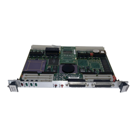
MVME162 Embedded Controller. Front Panel Switches and Indicators There are switches and LEDs on the front panel of the MVME162. The switches are RESET and ABORT. The RESET switch resets all onboard devices and drives SYSRESET* if the board is system controller. The RESET switch may be disabled by software. -
Page 17: Data Bus Structure
Functional Description Data Bus Structure The local data bus on the MVME162 is a 32-bit synchronous bus that is based on the MC68040 bus, and which supports burst transfers and snooping. The various local bus master and slave devices use the local bus to communicate. -
Page 18: Memory Options
The MVME162 provides jumpers (on J20) that allow either power source of the DS1210S to be connected to the VMEbus +5 V STDBY pin or to one cell of the onboard battery. - Page 19 The lifetime of the battery is very dependent on the ambient temperature of the board and the power-on duty cycle. The lithium battery supplied on the MVME162 should provide at least two years of backup time with the board powered off and with an ambient temperature of 40° C. If the power-on duty cycle is 50% (the board is powered on half of the time), the battery lifetime is four years.
- Page 20 EPROM and Flash The MVME162 implementation includes 1MB of Flash memory (an 8-Mbit Flash device organized as a 1M X 8, or four 2-Mbit Flash devices organized as 256Kbit x 8). For information on programming Flash, refer to the Intel documents listed in Related Documentation in this chapter.
-
Page 21: Battery Backed Up Ram And Clock
Functional Description Battery Backed Up RAM and Clock The MK48T08 RAM and clock chip is used on the MVME162. This chip pro- vides a time of day clock, oscillator, crystal, power failure detection, memory write protection, 8KB of RAM, and a battery in one 28-pin package. The clock provides seconds, minutes, hours, day, date, month, and year in BCD 24-hour format. - Page 22 NOTE: This port can be connected to the TX and RX clocks which may be present on the DB-25 connector. These connections are made via jumper header J11 on the MVME162 board. (The TxC and RxC clock lines are not available on the MVME712X transition modules.)
- Page 23 Port B is routed, via the SIM, to: The DB-25 connector marked SERIAL PORT 2 on the front panel of the MVME162. SERIAL PORT 2 will be an EIA-232-D DCE or DTE port, or an EIA-530 DCE or DTE port, depending upon which SIM is installed.
- Page 24 Every MVME162 that has the Ethernet interface is assigned an Ethernet Station Address. The address is $08003E2xxxxx, where xxxxx is the unique 5-nibble number assigned to the board (i.e., every MVME162 has a different value for xxxxx ). Each board has an Ethernet Station Address displayed on a label attached to the VMEbus P2 connector.
-
Page 25: Local Resources
Because the watchdog timer function in the VMEchip2 is a superset of that function in the MCchip (system reset function), the timer in the VMEchip2 is used in all cases except for the version of the MVME162 which does not include the VMEbus interface ("No VMEbus Interface" option). -
Page 26: Local Bus Arbiter
The serial ports on the MVME162 are also connected to two 25-pin DB-25 female connectors J9 and J15 on the front panel. The four IPs connect to the MVME162 by four pairs of 1-20... -
Page 27: Local Bus Memory Map
The normal address range is defined by the Transfer Type (TT) signals on the local bus. On the MVME162, Transfer Types 0, 1, and 2 define the normal address range. Table 1-3 is the entire map from $00000000 to $FFFFFFFF. - Page 28 Not decoded $FFD00000 - $FFDFFFFF Not decoded $FFE00000 - $FFE7FFFF SRAM default 512KB $FFE80000 - $FFEFFFFF Not decoded 512KB $FFF00000 - $FFFEFFFF Local I/O D32-D8 878KB $FFFF0000 - $FFFFFFFF VMEbus A16 D32/D16 64KB 2, 4 1-22 MVME162 Embedded Controller Installation Guide...
- Page 29 Memory Maps NOTES: Reset enables the decoder for this space of the memory map so that it will decode address spaces $FF800000 - $FF9FFFFF and $00000000 - $003FFFFF. The decode at 0 must be disabled in the MCchip before DRAM is enabled.
- Page 30 MK48T08 (BBRAM, TOD clock) D32-D8 32KB $FFFC8000 - $FFFCBFFF MK48T08 & disable Flash writes D32-D8 16KB 1, 7 $FFFCC000 - $FFFCFFFF MK48T08 & enable Flash writes D32-D8 16KB 1, 7 $FFFD0000 - $FFFEFFFF reserved 128KB 1-24 MVME162 Embedded Controller Installation Guide...
-
Page 31: Vmebus Memory Map
Memory Maps NOTES: For a complete description of the register bits, refer to the MVME162 Embedded Controller Programmer’s Reference Guide or to the data sheet for the specific chip. The SCC is an 8-bit device located on an MCchip private data bus. Byte access is required. - Page 32 Board Level Hardware Description 1-26 MVME162 Embedded Controller Installation Guide...
-
Page 33: Hardware Preparation And Installation
Most other modifications are performed by setting bits in control registers after MVME162 has been installed in a system. (For more information on the MVME162 registers refer to the MVME162 Embedded Controller Programmer’s Reference Guide listed in Related... -
Page 34: Sim Selection
SERIAL PORT 2 For the location of SIM connector J10 on the MVME162, refer to Figure 2-1. Figure 2-2 illustrates the secondary side (bottom) of a serial interface module, showing the J1 connector which plugs into SIM connector J10 on the MVME162. - Page 35 Hardware Preparation MVME 162-XXX FAIL STAT RUN SCON FUSE SCSI ABORT RESET MVME162IG/D2A1...
- Page 36 Hardware Preparation and Installation Figure 2-1. MVME162 Switches, Headers, Connectors, Fuses, and LEDs Table 2-2. Serial Interface Module Part Numbers Model Configuration Part Number Standard Number EIA-232-D 01-W3846B SIM05 01-W3865B SIM06 EIA-530 01-W3868B SIM07 01-W3867B SIM08 SECONDARY SIDE 10922.00 9403 (2-2) Figure 2-2.
-
Page 37: System Controller Select Header (J1)
Installation of New SIM Observe the orientation of the connector keys on SIM connector J1 and MVME162 connector J10. Turn the SIM so that the keys line up and place it gently on connector J10, aligning the mounting holes at the SIM corners with the matching standoffs on the MVME162. -
Page 38: Synchronous Clock Select Header (J11) For Serial Port 1/Console
Hardware Preparation and Installation Synchronous Clock Select Header (J11) for Serial Port 1/Console The MVME162 is shipped from the factory with the SERIAL PORT 1/CONSOLE header configured for asynchronous communications (i.e., jumpers removed). To select synchronous communications for the SERIAL PORT 1/CONSOLE connection, install jumpers across pins 1 and 2 and pins 3 and 4. -
Page 39: Sram Battery Backup Source Select Header (J20)
EPROM Size Select Header (J21) The MVME162 is factory-configured for a 4Mbit EPROM (i.e., a jumper is installed across pins 2 and 3). To configure the MVME162 for an 8Mbit EPROM, install the jumper across pins 1 and 2. 4Mbit EPROM... -
Page 40: General Purpose Readable Jumpers Header (J22)
(jumper removed). They are not user-definable. See Chapter 3 for more information. In most cases, the MVME162 is shipped from the factory with J22 set to all zeros (jumpers on all pins). On boards built with the no-VMEbus option, however, no jumper is installed across pins 9-10. -
Page 41: Installation Instructions
Because of the varying requirements for each different kind of IP, Motorola does not supply these cables. – Bring the IP cables out the narrow slots in the MVME162 front panel and attach them to the appropriate external equipment, depending on the nature of the particular IP(s). - Page 42 IACK daisy-chain driver. – If you do not intend to use the MVME162 as system controller, it can occupy any unused double-height card slot. Slide the MVME162 into the selected card slot. Be sure the module is seated properly in the P1 and P2 connectors on the backplane.
-
Page 43: Description Of 162Bug
This member of the M68000 Firmware family is implemented on the MVME162 MC68040- or MC68LC040- based Embedded Controller, and is known as the MVME162BUG, or 162Bug. -
Page 44: 162Bug Implementation
(e.g., "GO"), then control may or may not return to 162Bug, depending on the outcome of the user program. If you have used one or more of Motorola’s other debugging packages, you will find the CISC 162Bug very similar. Some effort has also been made to make the interactive commands more consistent. -
Page 45: Installation And Startup
Installation and Startup Follow the steps below to operate 162Bug with the MVME162module. 162Bug is factory-installed in the Flash memory of the MVME162, except in the no- VMEbus case. Inserting or removing modules while power is applied aution could damage module components. - Page 46 Bit #7 (GPI7) Open to your application. Note that when the MVME162 comes up in a cold reset, 162Bug runs in Board Mode. Using the Environment (ENV) or MENU commands can make 162Bug run in System Mode. Refer to Appendix A.
- Page 47 1 and 2 for synchronous communication. If using an EPROM version of the 162Bug (e.g., in no-VMEbus, blank- Flash versions of the MVME162), install the EPROM device in socket U47. Be sure that the physical chip orientation is correct — that is, with the flattened corner of the EPROM aligned with the corresponding portion of the EPROM socket on the MVME162 module.
- Page 48 If possible, an appropriate message is displayed, and control then returns to the menu. 10. Before using the MVME162 after the initial installation, set the date and time using the following command line structure: 162-Bug> SET [ mmddyyhhmm ]|[<+/- CAL >;C ]...
- Page 49 Autoboot If you are using an EPROM version of the 162Bug (e.g., in no-VMEbus, blank-Flash versions of the MVME162) andyou wish to execute the debugger out of Flash memory rather than from EPROM in subsequent sessions, make sure that 162Bug is in Board Mode and copy the EPROM...
- Page 50 This leaves the second half of the Flash memory and the EPROM socket (U47) available for your use. The 162Bug is also available in EPROM if your application requires all of the Flash memory. Contact your Motorola sales office for assistance. This function is configured/enabled by the Environment...
-
Page 51: Network Boot
Network Boot Network Boot Network Auto Boot is a software routine contained in the 162Bug Flash/EPROM that provides a mechanism for booting an operating system using a network (local Ethernet interface) as the boot device. The Network Auto Boot routine automatically scans for controllers and devices in a specified sequence until a valid bootable device containing a boot media is found or the list is exhausted. - Page 52 COLD and WARM reset modes are available. By default, 162Bug is in COLD mode. During COLD reset, a total system initialization takes place, as if the MVME162 had just been powered up. All static variables (including disk device and controller parameters) are restored to their default states. The breakpoint table and offset registers are cleared.
-
Page 53: Sysfail* Assertion/Negation
Memory Requirements Many times it may be desirable to terminate a debugger command prior to its completion; for example, during the display of a large block of memory. Break allows you to terminate the command. SYSFAIL* Assertion/Negation Upon a reset/powerup condition the debugger asserts the VMEbus SYSFAIL* line (refer to the VMEbus specification). -
Page 54: Terminal Input/Output Control
162Bug stack and static variable space and the rest is reserved as user space. Whenever the MVME162 is reset, the target PC is initialized to the address corresponding to the beginning of the user space, and the target stack pointers are initialized to addresses within the user space, with the target Interrupt Stack Pointer (ISP) set to the top of the user space. - Page 55 Terminal Input/Output Control The presence of the caret ( ^ ) before a character indicates that the Control (CTRL) key must be held down while striking the character key. (cancel line) The cursor is backspaced to the beginning of the line. If the terminal port is configured with the hardcopy or TTY option (refer to command), then a carriage return and line feed is...
-
Page 56: Disk I/O Support
162Bug translates this into an equivalent sector specification, which is then passed on to the controller to initiate the transfer. If the conversion from blocks to sectors yields a fractional sector count, an error is returned and no data is transferred. 3-14 MVME162 Embedded Controller Installation Guide... -
Page 57: Device Probe Function
Disk I/O via 162Bug Commands These following 162Bug commands are provided for disk I/O. Detailed instructions for their use are found in the Debugging Package for Motorola 68K CISC CPUs User’s Manual. When a command is issued to a particular controller LUN and device LUN, these LUNs are remembered by 162Bug so that the next disk command defaults to use the same controller and device. -
Page 58: Disk I/O Via 162Bug System Calls
Disk control. This function is used to implement any special device control functions that cannot be accommodated easily with any of the other disk functions. Refer to the Debugging Package for Motorola 68K CISC CPUs User’s Manual for information on using these and other system calls. 3-16... -
Page 59: Default 162Bug Controller And Device Parameters
Refer to the system call descriptions in the Debugging Package for Motorola 68K CISC CPUs User’s Manual for details on the format and construction of these standardized "user" packets. -
Page 60: Disk I/O Error Codes
Datagram Protocol, or UDP) from sources to destinations, where sources and destinations are hosts identified by fixed length addresses. The UDP/IP protocols are necessary for the TFTP and BOOTP protocols; TFTP and BOOTP require a UDP/IP connection. 3-18 MVME162 Embedded Controller Installation Guide... - Page 61 Network I/O Support RARP/ARP Protocol Modules The Reverse Address Resolution Protocol (RARP) basically consists of an identity-less node broadcasting a "whoami" packet onto the Ethernet, and waiting for an answer. The RARP server fills an Ethernet reply packet up with the target’s Internet Address and sends it.
-
Page 62: Multiprocessor Support
Debugger General Information Multiprocessor Support The MVME162 dual-port RAM feature makes the shared RAM available to remote processors as well as to the local processor. This can be done by either of the following two methods. Either method can be enabled/disabled by the ENV command as its Remote Start Switch Method (refer to Appendix A). - Page 63 Multiprocessor Support The Multiprocessor Address Register (MPAR), located in shared RAM location of $804 offset from the base address the debugger loads it at, contains the second of two longwords used to control communication between processors. The MPAR contents specify the address at which execution for the remote processor is to begin if the MPCR contains a G or B.
-
Page 64: Gcsr Method
$FFF40100. The VMEbus base address for the GCSR depends on the group select value and the board select value programmed in the Local Control and Status Registers (LCSR) of the MVME162. The execution address is formed by reading the GCSR general purpose registers in the following manner:... -
Page 65: Manufacturing Test Process
If either string is in the first location of NVRAM ($FFFC0000), the test process starts. This note is to inform users about the manufacturing test process; it is not intended to instruct customers in its use. Motorola reserves the right to delete, change, or modify this process. MVME162IG/D2A1... - Page 66 Debugger General Information 3-24 MVME162 Embedded Controller Installation Guide...
-
Page 67: Set Environment To Bug/Operating System
Set Environment to Bug/Operating System Set Environment to Bug/Operating System ENV [;[D]] The ENV command allows you to interactively view/configure all Bug operational parameters that are kept in Battery Backed Up RAM (BBRAM), also known as Non-Volatile RAM (NVRAM). The operational parameters are saved in NVRAM and used whenever power is lost. - Page 68 Auto Boot Controller LUN LUN of a disk/tape controller module currently supported by the Bug. Default is $0. Auto Boot Device LUN LUN of a disk/tape device currently supported by the Bug. Default is $0. MVME162 Embedded Controller Installation Guide...
- Page 69 Table A-2. ENV Command Parameters (Continued) ENV Parameter and Options Default Meaning of Default Master Starting Address #3 00000000 Base address of the VMEbus resource that is accessible from the local bus. If enabled, the value is calculated as one more than the calculated size of memory.
- Page 70 Local Bus Time Out Code This controls the local bus timeout. Default $02 = 256 µs. VMEbus Access Time Out Code This controls the local bus to VMEbus access timeout. Default $02 = 32 ms. A-12 MVME162 Embedded Controller Installation Guide...
Need help?
Do you have a question about the MVME162 and is the answer not in the manual?
Questions and answers