Table of Contents
Advertisement
Quick Links
Advertisement
Table of Contents

Related Manuals for Aaeon UPC-Plus


Summary of Contents for Aaeon UPC-Plus
- Page 1 UPC-Plus Maker Board User’s Manual 1 Last Updated: October 25, 2018...
- Page 2 AAEON assumes no liabilities resulting from errors or omissions in this document, or from the use of the information contained herein. AAEON reserves the right to make changes in the product design without notice to its users.
- Page 3 Acknowledgement All other products’ name or trademarks are properties of their respective owners. Microsoft Windows is a registered trademark of Microsoft Corp. Intel, Pentium, Celeron, and Xeon are registered trademarks of Intel Corporation Core, Atom are trademarks of Intel Corporation ...
- Page 4 Packing List Before setting up your product, please make sure the following items have been shipped: Item Quantity UPC-Plus If any of these items are missing or damaged, please contact your distributor or sales representative immediately. Preface...
- Page 5 (if any), its specifications, dimensions, jumper/connector settings/definitions, and driver installation instructions (if any), to facilitate users in setting up their product. Users may refer to the AAEON.com for the latest version of this document. Preface...
- Page 6 Safety Precautions Please read the following safety instructions carefully. It is advised that you keep this manual for future references All cautions and warnings on the device should be noted. Make sure the power source matches the power rating of the device. Position the power cord so that people cannot step on it.
- Page 7 If any of the following situations arises, please the contact our service personnel: Damaged power cord or plug Liquid intrusion to the device iii. Exposure to moisture Device is not working as expected or in a manner as described in this manual The device is dropped or damaged Any obvious signs of damage displayed on the device...
- Page 8 FCC Statement This equipment has been tested and found to comply with the limits for a Class B digital device, pursuant to part 15 of the FCC Rules. These limits are designed to provide reasonable protection against harmful interference in a residential installation. This equipment generates, uses and can radiate radio frequency energy and, if not installed and used in accordance with the instructions, may cause harmful interference to radio communications.
- Page 9 This equipment complies with FCC radiation exposure limits set forth for an uncontrolled environment. This equipment should be installed and operated with minimum distance 20cm between the radiator & your body. This device complies with Part 15 of FCC rules. Operation is subject to the following two conditions: (1) this device may not cause harmful interference and (2) this device must accept any interference received, including interference that may cause undesired operation.
- Page 10 China RoHS Requirements (CN) 产品中有毒有害物质或元素名称及含量 AAEON Main Board/ Daughter Board/ Backplane 有毒有害物质或元素 部件名称 铅 汞 镉 六价铬 多溴联苯 多溴二苯醚 (Pb) (Hg) (Cd) (Cr(VI)) (PBB) (PBDE) 印刷电路板 ○ ○ ○ ○ ○ ○ 及其电子组件 外部信号 ○ ○ ○ ○ ○ ○...
- Page 11 China RoHS Requirement (EN) Poisonous or Hazardous Substances or Elements in Products AAEON Main Board/ Daughter Board/ Backplane Poisonous or Hazardous Substances or Elements Hexavalent Polybrominated Polybrominated Component Lead Mercury Cadmium Chromium Biphenyls Diphenyl Ethers (Pb) (Hg) (Cd) (Cr(VI)) (PBB) (PBDE) PCB &...
-
Page 12: Table Of Contents
Table of Contents Chapter 1 - Product Specifications..................1 Specifications ......................2 Chapter 2 – Hardware Information ..................5 Dimensions ....................... 6 Jumpers and Connectors ..................7 List of Switches and Connectors................8 2.3.1 Power Button (SW1) ..................10 2.3.2 Power Button (CN1) ................ -
Page 13: Chapter 1 - Product Specifications
Chapter 1 Chapter 1 - Product Specifications... -
Page 14: Specifications
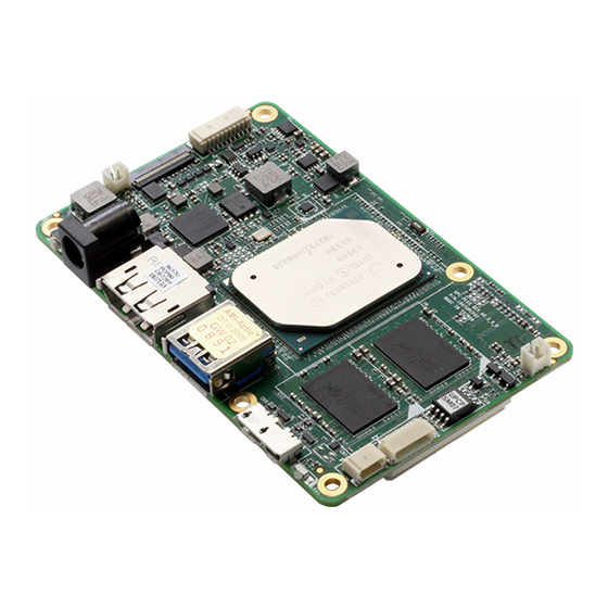
Specifications System Intel® Apollo Lake SoC E3930/E3940/E3950 CPU/Chipset Onboard Single/Dual Channel LPDDR4 Memory memory, Max 8GB Intel® HD Graphics Graphics 1x DP 1x Full eDP 1x eMMC ver 5.0 (32GB/64GB/128GB) Storage Onboard WIFI 802.11 a/b/g/n/ac + BT 4.2 WiFi/BT ... - Page 15 Docking Connector 2 100 pin: 1. 12V, GND 2. DDIx1 (for 3rd display on HDMI / DP) 3. 3x PCIex1 4. 2x PCIex1 or USB3.0 5. 1xSATA1 or USB 3.0 6. 1x SATA0 7. 3xUSB2.0 1x eDP with Backlight control Header Internal I/O Connectors ...
- Page 16 Others 12V DC in Power 90 mm × 56 mm Form Factor 0°C -60°C Operating Temperature 0% ~ 90% relative humidity, non-condensing Operating Humidity CE,FCC ClassB Certification Win 10, OS Support Linux (UbiLinux, Ubuntu, Yocto) Chapter 1 –...
-
Page 17: Chapter 2 - Hardware Information
Chapter 2 Chapter 2 – Hardware Information... -
Page 18: Dimensions
Dimensions Chapter 2 – Hardware Information... -
Page 19: Jumpers And Connectors
Jumpers and Connectors Component side Solder side Chapter 2 – Hardware Information... -
Page 20: List Of Switches And Connectors
List of Switches and Connectors Please refer to the table below for all of the board’s jumpers that you can configure for your application Connector Type Reference Function (TF)Push Button PWR button Switch.3P .12VDC.50mA.500mohm.Black.SMD.HCH.PTS- (TF)WAFER BOX.2P .180D(M).DIP .1.25mm.PINREX.712-71-02TW01 Internal USB (TF)Wafer Box.10P .90D(M).SMD.1.0mm.PINREX.710-74-10TWR6 UART... - Page 21 (TF)Board-Board CN10 DOCKING I Connector.100P .180D(M).Pitch=0.5mm.H=5.3mm.SMD. Panasonic.AXK6S00647YG (TF)FPC/FFC Conn..31P .90D(F).SMD.0.3mm.Dual CN11 MIPI CSI Contact.Panasonic.AYF333135 (TF)Board-Board CN12 DOCKING II Connector.100P .180D(M).Pitch=0.5mm.H=5.3mm.SMD. Panasonic.AXK6S00647YG (TF)FPC/FFC CN13 MIPI CSI 2CH Conn.21P .90D(F).SMD.0.6mm.Hirose.FH35C-21S-0.3SH W(50) (TF)WAFER PWR Button CN14 BOX.2P .90D(M).SMD.1.0mm.W/Cap.PINREX.710-74-02T Pin Header SYSTEM (TF)LED.3.0*1.0*1.0mm. Blue.SMD.LITEON. LED1 LTST-S320TBKT Indicator...
-
Page 22: Power Button (Sw1)
2.3.1 Power Button (SW1) Signal Signal PMU_PWRBTN_N 2.3.2 Power Button (CN1) Signal Signal EXT_PWRBTN# LED+ LED- Chapter 2 – Hardware Information... -
Page 23: Internal Usb Uart (Cn2)
2.3.3 Internal USB UART (CN2) Signal Signal USB2_DN6 USB2_DP6 USB2_DN7 USB2_DP7 UART0_RXD_3V3 UART0_TXD_3V3 Chapter 2 – Hardware Information... -
Page 24: Jtag (Cn3)
2.3.4 JTAG (CN3) Signal Signal EDP_TXP_0 EDP_TXN_0 EDP_TXP_1 EDP_TXN_1 EDP_TXP_2 EDP_TXN_2 EDP_TXP_3 EDP_TXN_3 EDP_AUXP EDP_AUXN EDP_HPD_CONN DDI0_BKLT_CTRL DDI0_VDD_EN DDI0_BKLT_EN I2C_3V3_SCL7 I2C_3V3_SDA7 +3.3V +3.3V +3.3V +3.3V +3.3V Chapter 2 – Hardware Information... -
Page 25: Bios Program (Cn4)
2.3.5 BIOS PROGRAM (CN4) Signal Signal SPI_MISO SPI_CLK +VCC_SPI SPI_MOSI SPI_CS0# 2.3.6 RTC (CN5) Signal Signal RTC_VCC Chapter 2 – Hardware Information... -
Page 26: Usb 3.0 (Cn6)
2.3.7 USB 3.0 (CN6) Signal Signal +V5P0_USB_1 USB2_C_DN1 USB2_C_DP1 USB3_RXN_CON_P1 USB3_RXP_CON_P1 USB3_TXN_CON_P1 USB3_TXP_CON_P1 2.3.8 CASH DRAWER (CN7) Signal Signal DDI1_TXP_DP_0 DDI1_TXN_DP_0 DDI1_TXP_DP_1 DDI1_TXN_DP_1 DDI1_TXP_DP_2 DDI1_TXN_DP_2 DDI1_TXP_DP_3 Chapter 2 – Hardware Information... -
Page 27: Power Input (Cn8)
DDI1_TXN_DP_3 DDI1_AUXP_C DDI1_AUXP_C DDI1_AUXN_C DDI1_HPD +3.3V 2.3.9 Power input (CN8) Signal Signal +12V Chapter 2 – Hardware Information... -
Page 28: Micro Usb3.0 (Cn9)
2.3.10 Micro USB3.0 (CN9) Signal Signal +V5P0_USB_OTG USB2_C_DN0 USB2_C_DP0 USB_OTG_R_ID USB3_RXN_CON_P0 USB3_RXP_CON_P0 USB3_TXN_CON_P0 USB3_TXP_CON_P0 2.3.11 DOCKING I (CN10) Signal Signal +V5A +V5A +V5A +V5A +V5A +V5A +V5A +V5A BUF_PLT_RST# LPSS_UART1_RTS PMU_PWRBTN_N LPSS_UART1_CTS Chapter 2 – Hardware Information... - Page 29 PM_SLP_S3#_3P3 LPSS_UART1_TXD PCIE_CLKREQ3# LPSS_UART1_RXD PCIE_WAKE3_N CPU_prog_JTAG_TDO SIO_SPI_0_TXD CPU_prog_JTAG_TMS SIO_SPI_0_RXD HDMI1_CEC_D SIO_SPI_0_CLK CPU_prog_JTAG_TCK SIO_SPI_0_FS0 CPU_prog_JTAG_TDI SIO_SPI_0_FS1 ISH_GPIO_0 ISH_GPIO_1 LPC_R_AD0 ISH_GPIO_2 LPC_R_AD1 ISH_GPIO_3 LPC_R_AD2 ISH_GPIO_4 LPC_R_AD3 ISH_GPIO_5 ISH_GPIO_6 AVS_I2S2_MCLK PWM0 AVS_I2S2_WS_SYNC PWM1 AVS_I2S2_SDI AVS_I2S2_SDO I2C_SDA6 I2C_SCL6 PCIE_P5_USB3_P2_TXP PCIE_P5_USB3_P2_TXN AVS_I2S2_BCLK BT_HOST_WAKE PCIE_P5_USB3_P2_RXP PCIE_P5_USB3_P2_RXN USB2_DP2 USB2_DN2 PCIE_REFCLK3_P...
- Page 30 I2C_SDA0 ISH_GPIO_7 I2C_SCL0 ISH_GPIO_8 ISH_GPIO_9 I2C_SDA1 ISH_GPIO_10 I2C_SCL1 ISH_GPIO_11 ISH_GPIO_12 GPIO_2 ISH_GPIO_13 GPIO_3 ISH_GPIO_14 PMIC_IRQ_N LPC_FRAME_R FPGA_CLR LPC_R_CLKOUT0 LPC_CLKRU_N FPGA_RST INT_SERIRQ_R FPGA_OE CONFIG_SEL FPGA_fw_reload Chapter 2 – Hardware Information...
-
Page 31: Mipi Csi (Cn11)
2.3.12 (CN11) MIPI CSI Signal Signal CAM1_RST_N I2C_SDA4 I2C_SCL4 OSC_CLK_OUT_2 USB3_TXN_CON_P0 MCSI_RX_DATAP_0 MCSI_RX_DATAP_0 MCSI_RX_DATAP_1 MCSI_RX_CLKN_0 MCSI_RX_CLKP_0 MCSI_RX_DATAN_2 MCSI_RX_DATAP_2 MCSI_RX_DATAN_3 MCSI_RX_DATAP_3 +AVDD_CAM GND_CAM +V1P8_CAM +V2P8_CAM +V2P8_CAM Chapter 2 – Hardware Information... -
Page 32: Docking Ii (Cn12)
2.3.13 DOCKING II (CN12) Signal Signal +12V +12V +12V +12V +12V +12V +12V +12V DDI0_HPD DDI0_TXP_1 DDI0_TXP_0 DDI0_TXN_1 DDI0_TXN_0 DDI0_TXP_2 DDI0_TXP_3 DDI0_TXN_2 DDI0_TXN_3 DDI0_AUXP DDI0_DDCCLK DDI0_AUXN DDI0_DDCDATA PCIE_REFCLK0_P PCIE_REFCLK1_P PCIE_REFCLK0_N PCIE_REFCLK1_N PCIE_RXP0 PCIE_RXP1 PCIE_RXN0 PCIE_RXN1 Chapter 2 – Hardware Information... - Page 33 PCIE_TXP0 PCIE_TXP1 PCIE_TXN0 PCIE_TXN1 PCIE_REFCLK2_P PCIE_P3_USB3_P4_TXP PCIE_REFCLK2_N PCIE_P3_USB3_P4_TXN PCIE_TXP2 PCIE_P3_USB3_P4_RXP PCIE_TXN2 PCIE_P3_USB3_P4_RXN PCIE_RXP2 SATA_P1_USB3_P5_RXN PCIE_RXN2 SATA_P1_USB3_P5_RXP PCIE_P4_USB3_P3_TXP SATA_P1_USB3_P5_TXN PCIE_P4_USB3_P3_TXN SATA_P1_USB3_P5_TXP PCIE_P4_USB3_P3_RXP SATA_RXN0 PCIE_P4_USB3_P3_RXN SATA_RXP0 USB2_DP3 SATA_TXP0 USB2_DN3 SATA_TXN0 USB2_DP4 USB2_DP5 USB2_DN4 USB2_DN5 PWRON_PNLVDDEN SATA_LED_N PMU_RSTBTN_N DDI0_BKLTCTL PCIE_WAKE0_N PCIE_CLKREQ0# PCIE_WAKE1_N PCIE_CLKREQ1# Chapter 2 –...
-
Page 34: Mipi Csi 2Ch (Cn13)
PCIE_WAKE2_N PCIE_CLKREQ2# 2.3.14 MIPI CSI 2CH (CN13) Signal Signal MCSI_DN_1 MCSI_DP_1 MCSI_CLKN_0 MCSI_CLKP_0 MCSI_DN_0 MCSI_DP_0 +V1P2_CAM +V1P8_CAM OSC_CLK_OUT_3 I2C_SCL4 I2C_SDA4 CAM2_RST_N FLASH_RESET_N +V2P8_CAM GND_CAM Chapter 2 – Hardware Information... -
Page 35: Pwr Button Pin Header (Cn14)
2.3.15 PWR Button Pin Header (CN14) Signal Signal PWRBTN_N RSTBTN_N Chapter 2 – Hardware Information... -
Page 36: Chapter 3 - Drivers Installation
Chapter 3 Chapter 3 – Drivers Installation... -
Page 37: Driver Download And Installation
Driver Download and Installation *Please access https://up-community.org and go to the Downloads section to find the relevant driver. Chapter 3 – Drivers Installation...
Need help?
Do you have a question about the UPC-Plus and is the answer not in the manual?
Questions and answers