
Subscribe to Our Youtube Channel
Related Manuals for Aaeon ?COM-BT


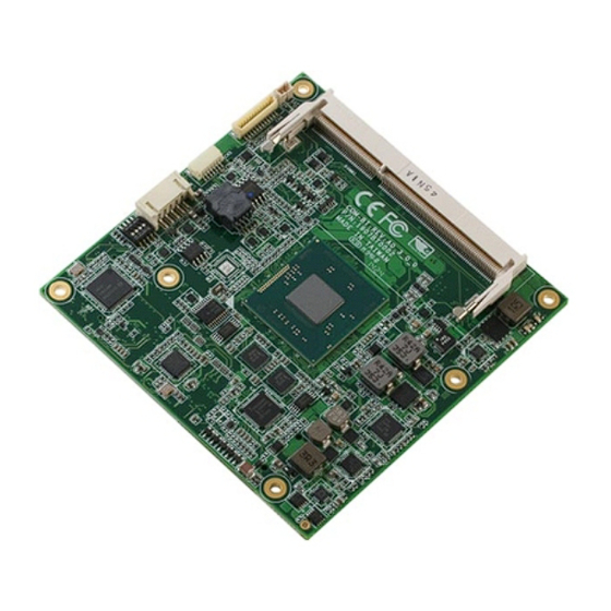
Summary of Contents for Aaeon ?COM-BT
- Page 1 μ C O M - B T S M AR C M o d u l e μCOM-BT ® ® Intel Atom™/ Celeron Processor Onboard Memory 2GB Gigabit Ethernet 2 SATA 2 USB 2.0, 1 USB 3.0, 3 PCI-E[x1] LVDS, HDMI, HD Audio μCOM-BT Rev.
- Page 2 AAEON assumes no liabilities resulting from errors or omissions in this document, or from the use of the information contained herein. AAEON reserves the right to make changes in the product design without notice to its users.
- Page 3 μ C O M - B T S M AR C M o d u l e Acknowledgments All other products’ name or trademarks are properties of their respective owners. AMI is a trademark of American Megatrends Inc. ® ®...
- Page 4 μ C O M - B T S M AR C M o d u l e Packing List Before you begin installing your card, please make sure that the following materials have been shipped: • M2.5 Screw • DVD-ROM for drivers and manual (in PDF format) •...
- Page 5 μ C O M - B T S M AR C M o d u l e China RoHS Requirements 产品中有毒有害物质或元素名称及含量 AAEON Main Board/ Daughter Board/ Backplane 有毒有害物质或元素 部件名称 铅 汞 镉 六价铬 多溴联苯 多溴二苯醚 (Pb) (Hg) (Cd) (Cr(VI)) (PBB) (PBDE) 印刷电路板...
- Page 6 μ C O M - B T S M AR C M o d u l e China RoHS Requirements Poisonous or Hazardous Substances or Elements in Products AAEON Main Board/ Daughter Board/ Backplane Poisonous or Hazardous Substances or Elements Hexavalent Polybrominated...
-
Page 7: Table Of Contents
μ C O M - B T S M AR C M o d u l e Contents Chapter 1 General Information 1.1 Introduction ..............1-2 1.2 Features ..............1-3 1.3 Specifications ............1-4 Chapter 2 Quick Installation Guide 2.1 Safety Precautions ............ 2-2 2.2 Mechanical Drawings .......... - Page 8 μ C O M - B T S M AR C M o d u l e Appendix B I/O Information B.1 I/O Address Map ............ B-2 B.2 Memory Address Map ..........B-4 B.3 IRQ Mapping Chart ..........B-5 Appendix C Programming the Digital I/O C.1 Digital I/O Sample Program ........
-
Page 9: Chapter 1 General Information
μ C O M - B T S M AR C M o d u l e Chapter General Information 1- 1 Chapter 1 General Information... -
Page 10: Introduction
Users may refer to the AAEON.com for the latest version of this document. 1- 2 Chapter 1 General Information... -
Page 11: Features
μ C O M - B T S M AR C M o d u l e 1.2 Features ® ® Onboard Intel Atom™ E3800 Series or Celeron N2807 Processor SoC Onboard DDR3L 2 GB Memory Gigabit Ethernet ... -
Page 12: Specifications
μ C O M - B T S M AR C M o d u l e 1.3 Specifications System Form Factor SMARC, 82 x 50 mm ® ® Processor Intel Atom™ E3800 Series or Celeron N2807 Processor SoC ... - Page 13 μ C O M - B T S M AR C M o d u l e Power Requirement Standard: DC 5V Board Size 3.23”(L) x 1.97”(W) (82mm x 50mm) Gross Weight Operating Standard: 32°F ~ 140°F (0°C ~ 60°C) Temperature Optional: -40°F ~ 185°F (-40°C ~ 80°C) ...
- Page 14 μ C O M - B T S M AR C M o d u l e TX/RX) USB 3.0 x 1 USB 2.0 x 2 Audio High Definition Audio x 1 GPIO 12 bit, 1.8V (1 share with HDA , 2 share with MiPi) 1- 6 Chapter 1 General Information...
-
Page 15: Chapter 2 Quick Installation Guide
μ C O M - B T S M AR C M o d u l e Chapter Quick Installation Guide Chapter 2 Quick Installation Guide... -
Page 16: Safety Precautions
μ C O M - B T S M AR C M o d u l e 2.1 Safety Precautions Always completely disconnect the power cord from your board whenever you are working on it. Do not make connections while the power is on, because a sudden rush of power can damage sensitive electronic components. -
Page 17: Mechanical Drawings
μ C O M - B T S M AR C M o d u l e 2.2 Mechanical Drawings Component Side ( 3 . 6 0 ) 4 . 0 0 ( 3 . 6 0 ) 5 0 . 0 0 4 . - Page 18 μ C O M - B T S M AR C M o d u l e Solder Side ( 3 . 6 0 ) 4 6 . 0 0 4 2 . 4 2 4 5 . 0 9 2 9 .
- Page 19 μ C O M - B T S M AR C M o d u l e Heat Sink 2 - 5 Chapter 2 Quick Installation Guide...
- Page 20 μ C O M - B T S M AR C M o d u l e Heat Spreader 2 - 6 Chapter 2 Quick Installation Guide...
-
Page 21: List Of Jumpers
μ C O M - B T S M AR C M o d u l e 2.3 List of Jumpers The board has a number of jumpers/ connectors/ switches for configuring your system for your application. Please refer to the tables below of their functions: Label Function Boot Mode Selection... -
Page 22: List Of Connectors
μ C O M - B T S M AR C M o d u l e 2.4 List of Connectors The board has a number of jumpers/ connectors/ switches for configuring your system for your application. Please refer to the tables below of their functions: Label Function BAT1A... -
Page 23: Rtc Battery Connector (Bat1)
μ C O M - B T S M AR C M o d u l e 2.5 Boot Mode Selection (SW1) Clear RTC RTC normal mode(Default) ATX(Default) 2.6 RTC Battery Connector (BAT1) Pin Name Signal Type Signal Level 2 - 9 Chapter 2 Quick Installation Guide... -
Page 24: Mxm 314 Pin Definitions
μ C O M - B T S M AR C M o d u l e 2.7 MXM 314 Pin Definitions Signal Signal CSI1_CK+ CSI1_CK- CAM_I2C_CLK CSI1_D0+ CAM_I2C_DATA CSI1_D0+ CSI0_CK+ CSI0_CK- CSI1_D1+ CSI1_D1- CSI0_D0+ CSI0_D0+ CSI1_D2+ CSI1_D2- CSI1_D3+ CSI1_D3- PM_SLP_S3# PM_SLP_S4# GBE_MDI3-... - Page 25 μ C O M - B T S M AR C M o d u l e GBE_LINK1000# GBE_MDI2- GBE_MDI2+ GBE_LINK_ACT# GBE_MDI1- GBE_MDI1+ GBE_MDI0- GBE_MDI0+ SDIO_WP SDIO_CMD SDIO_CD# SDIO_CK SDIO_PWR_EN CB_MCLK SDIO_D0 I2S0_LRCK SDIO_D1 I2S0_SDOUT SDIO_D2 I2S0_SDIN SDIO_D3 I2S0_CK 2 - 11 Chapter 2 Quick Installation Guide...
- Page 26 μ C O M - B T S M AR C M o d u l e SATA_TX+ I2C_GP_CLK SATA_TX- I2C_GP_DAT HDA_SYNC SATA_RX+ HDA_SDO SATA_RX- HDA_SDI HDA_CK SPI1_CS0# SATA_ACT# SPI1_CK SPI1_DIN SPI1_DO USB0+ USB0- USB0_EN_OC# USB3_TX0_P USB0_VBUS_DET USB3_TX0_N USB0_OTG_ID USB1+ USB3_RX0_P USB1- USB3_RX0_N...
- Page 27 μ C O M - B T S M AR C M o d u l e USB2- USB2_EN_OC# SATA_TXP1 PCIE_C_PRSNT# SATA_TXN1 PCIE_B_PRSNT# PCIE_A_PRSNT# SATA_RXP1 SATA_RXN1 PCIE_A_RST PCIE_B_RST PCIE_C_CK_REQ# PCIE_C_RST PCIE_B_CK_REQ# PCIE_C_RX+ PCIE_A_CK_REQ# PCIE_C_RX- PCIE_C_REFCK+ PCIE_C_TX+ PCIE_C_REFCK- PCIE_C_TX- PCIE_A_REFCK+ PCIE_B_REFCK+ PCIE_A_REFCK- PCIE_B_REFCK- PCIE_A_RX+...
- Page 28 μ C O M - B T S M AR C M o d u l e HDMI_D2+ HDMI_D2- HDMI_D1+ HDMI_D1- HDMI_D0+ HDMI_D0- S100 P100 S101 P101 HDMI_CK+ S102 P102 HDMI_CK- S103 P103 S104 P104 HDMI_HPD S105 P105 HDMI_CTRL_CK S106 P106 HDMI_CTRL_DAT S107...
- Page 29 μ C O M - B T S M AR C M o d u l e P116 GPIO8 S117 P117 GPIO9 S118 P118 GPIO10 S119 P119 GPIO11 S120 P120 S121 P121 I2C_PM_CK S122 P122 I2C_PM_DAT S123 P123 BOOT_SEL0# S124 P124 BOOT_SEL1# S125...
- Page 30 μ C O M - B T S M AR C M o d u l e P140 S141 LCD_BKLT_PWM P141 S142 P142 S143 P143 S144 P144 S145 WDT_TIME_OUT# P145 S146 PCIE_WAKE# P146 S147 VDD_RTC P147 VDD_IN S148 LID# P148 VDD_IN S149 SLEEP#...
-
Page 31: Chapter 3 Ami Bios Setup
μ C O M - B T S M AR C M o d u l e Chapter BIOS Setup Chapter 3 AMI BIOS Setup 3-1... -
Page 32: System Test And Initialization
μ C O M - B T S M AR C M o d u l e 3.1 System Test and Iinitializations These routines test and initialize board hardware. If the routines encounter an error during the tests, you will either hear a few short beeps or see an error message on the screen. -
Page 33: Ami Bios Setup
μ C O M - B T S M AR C M o d u l e 3.2 AMI BIOS Setup AMI BIOS ROM has a built-in Setup program that allows users to modify the basic system configuration. This type of information is stored in battery-backed CMOS RAM and BIOS NVRAM so that it retains the Setup information when the power is turned off. - Page 34 μ C O M - B T S M AR C M o d u l e Main Press ‘Delete’ Key to enter Setup Chapter 3 AMI BIOS Setup 3-4...
- Page 35 μ C O M - B T S M AR C M o d u l e Advanced Chapter 3 AMI BIOS Setup 3-5...
- Page 36 μ C O M - B T S M AR C M o d u l e Advanced -> Power Management Options summary: Power Mode ATX Type Optimal Default, Failsafe Default AT Type Select power supply mode Restore AC Power Off Power Loss Power On Optimal Default, Failsafe Default...
- Page 37 μ C O M - B T S M AR C M o d u l e Auto Disable Optimal Default, Failsafe Default Configuration Enables or Disables BIOS ACPI Auto Configuration Enable Enable Optimal Default, Failsafe Default Hibernation Disable Enables or Disables System ability to Hibernate (OS/S4 Sleep State). This option may be not effective with some OS ACPI Sleep State Suspend Disabled Optimal Default, Failsafe Default...
- Page 38 μ C O M - B T S M AR C M o d u l e Advanced -> Power Management -> S5 RTC Wake Settings Options summary: Wake system with Fixed Time Enable Optimal Default, Failsafe Default Disable Enable or disable System wake on alarm event. Wake up time is setting by following settings.
- Page 39 μ C O M - B T S M AR C M o d u l e Wake up hour 0-23 Wake up minute 0-59 Wake up second 0-59 Wake system with Dynamic Enable Time Optimal Default, Failsafe Default Disable Enable or disable System wake on alarm event.
- Page 40 μ C O M - B T S M AR C M o d u l e Advanced -> Digital IO Options summary: Pin 1/2/3/4/5/6/7 Input Optimal Default, Failsafe Default Output Set DIO Port 1/2/3/4/5/6/7 as Input or Output Pin 8/9/10/11 Input Optimal Default, Failsafe Default Output...
- Page 41 μ C O M - B T S M AR C M o d u l e Advanced -> H/W Monitor Note: The two CPU temperature sensors are located by the edge of the CPU and the back of the MCB respectively. Chapter 3 AMI BIOS Setup 3-11...
- Page 42 μ C O M - B T S M AR C M o d u l e Advanced -> CPU Configuration Options summary: Intel Disabled Virtualization Enabled Optimal Default, Failsafe Default Technology When enabled, a VMM can utilize the additional hardware capabilities provided by Vander pool Technology Chapter 3 AMI BIOS Setup 3-12...
- Page 43 μ C O M - B T S M AR C M o d u l e Advanced -> CPU Configuration Socket 0 CPU Information Chapter 3 AMI BIOS Setup 3-13...
- Page 44 μ C O M - B T S M AR C M o d u l e Advanced -> IDE Configuration Options summary: Serial-ATA(SATA) Enabled Default Disable SATA Speed Support Gen1 Gen2 Default SATA ODD Port Port0 ODD Port1 ODD No ODD Default SATA Mode...
- Page 45 μ C O M - B T S M AR C M o d u l e IDE: Configure SATA controllers as legacy IDE AHCI: Configure SATA controllers to operate in AHCI mode Serial-ATA Port0/1 Enabled Default Disable SATA Port0/1 HotPlug Enabled Disable Default...
- Page 46 μ C O M - B T S M AR C M o d u l e Advanced -> CSM Configuration Options summary: CSM Support Enabled Default Disable Boot option filter UEFI and Default Legacy Legacy UEFI Storage & Video Do not launch UEFI Default...
- Page 47 μ C O M - B T S M AR C M o d u l e Other PCI devices UEFI Default Legacy Chapter 3 AMI BIOS Setup 3-17...
- Page 48 μ C O M - B T S M AR C M o d u l e Advanced -> USB Configuration Options summary: Legacy USB Support Enabled Optimal Default, Failsafe Default Disabled Auto Enables BIOS Support for Legacy USB Support. When enabled, USB can be functional in legacy environment like DOS.
- Page 49 μ C O M - B T S M AR C M o d u l e Device Name (Emulation Auto Optimal Default, Failsafe Default Type) Floppy Forced FDD Hard Disk CDROM If Auto. USB devices less than 530MB will be emulated as Floppy and remaining as Floppy and remaining as hard drive.
- Page 50 μ C O M - B T S M AR C M o d u l e Advanced -> LPSS & SCC Configuration Options summary: LPSS & SCC Devices ACPI mode Mode PCI mode Default LPSS & SCC Devices Mode Settings SCC eMMC Support Enabled eMMC 4.5 Support...
- Page 51 μ C O M - B T S M AR C M o d u l e Disabled SCC eMMC Support Enable/Disable SCC eMMC 4.5 DDR50 Enabled Default Support Disabled SCC eMMC 4.5 DDR50 Support Enable/Disable SCC eMMC 4.5 HS200 Enabled Support Default...
- Page 52 μ C O M - B T S M AR C M o d u l e Per chipset spec, there is chance that SD card can’t be recognized properly when set to high speed. (DDR50) The issue doesn’t occur at low speed setting.
- Page 53 μ C O M - B T S M AR C M o d u l e Chipset Chapter 3 AMI BIOS Setup 3-23...
- Page 54 μ C O M - B T S M AR C M o d u l e Chipset -> Host Bridge Primary Boot Display VBIOS Default Default DP/HDMI Chapter 3 AMI BIOS Setup 3-24...
- Page 55 μ C O M - B T S M AR C M o d u l e Chipset -> Host Bridge -> IGD – LCD Control Chapter 3 AMI BIOS Setup 3-25...
- Page 56 μ C O M - B T S M AR C M o d u l e Chipset -> South Bridge Chapter 3 AMI BIOS Setup 3-26...
- Page 57 μ C O M - B T S M AR C M o d u l e Chipset -> South Bridge -> Azalia HD Audio Options summary: Audio Controller Disabled Default Enabled Control Detection of the Azalia device. Disabled = Azalia will be unconditionally disabled. Enabled = Azalia will be unconditionally Enabled.
- Page 58 μ C O M - B T S M AR C M o d u l e LPE Audio ACPI mode Select LPE Audio ACPI mode or PCI mode Azalia HDMI codec Disabled Default Enabled Enable/Disable internal HDMI codec for Azalia HDMI Port Disabled Enabled...
- Page 59 μ C O M - B T S M AR C M o d u l e Chipset -> South Bridge -> USB Configuration Options summary: USB OTG Support PCI mode Default Disabled Enable/Disable USB OTG Support XHCI Mode Enabled Disabled Default Auto...
- Page 60 μ C O M - B T S M AR C M o d u l e Disabled Control each of the USB ports (0~3). Enable: Enable USB per port Disable: Use USB port X settings USB Port0/1/2/3 Enabled Default Disabled Enable/Disable USB Port0/1/2/3 Chapter 3 AMI BIOS Setup 3-30...
- Page 61 μ C O M - B T S M AR C M o d u l e Chipset -> South Bridge -> PCI Express Configuration Options summary: PCI Express Root Port Disabled 0/1/2/3 Enabled Optimal Default, Failsafe Default Enabling/Disabling the PCI Express root ports Hot Plug Disabled Default...
- Page 62 μ C O M - B T S M AR C M o d u l e Gen2 Gen1 Configure PCIe Port Speed Note: PCIe Port 0 is used for LAN Chapter 3 AMI BIOS Setup 3-32...
- Page 63 μ C O M - B T S M AR C M o d u l e Security Setup submenu: Security Change User/Supervisor Password You can install a Supervisor password, and if you install a supervisor password, you can then install a user password. A user password does not provide access to many of the features in the Setup utility.
- Page 64 μ C O M - B T S M AR C M o d u l e password is required at boot time, or when the user enters the Setup utility. Removing the Password Highlight this item and type in the current password. At the next dialog box press Enter to disable password protection.
- Page 65 μ C O M - B T S M AR C M o d u l e Boot Options summary: Quiet Boot Disabled Enabled Default En/Disable showing boot logo. Launch i210/i211 PXE Disabled Default OpROM Enabled En/Disable PXE boot for i210/i211 LAN Chapter 3 AMI BIOS Setup 3-35...
- Page 66 μ C O M - B T S M AR C M o d u l e Exit Chapter 3 AMI BIOS Setup 3-36...
-
Page 67: Chapter 4 Driver Installation
μ C O M - B T S M AR C M o d u l e Chapter Driver Installation 4 -1 Chapter 4 Driver Installation... - Page 68 μ C O M - B T S M AR C M o d u l e The μCOM-BT comes with a driver disk that contains all drivers and utilities you need to setup your product. Insert the disk and the installation guide will start automatically. If it doesn’t, please follow the sequence below to install the drivers.
- Page 69 μ C O M - B T S M AR C M o d u l e 4.1 Installation Insert the μCOM-BT driver disk into the disk drive and install the drivers from Step 1 to Step 9 in order. Step 1 –...
- Page 70 μ C O M - B T S M AR C M o d u l e Step 4 – Install Audio Driver 1. Open the STEP4 - Audio folder followed by win7_8-32_64_R273.exe 2. Follow the instructions 3. Drivers will be installed automatically Step 5 –...
- Page 71 μ C O M - B T S M AR C M o d u l e Step 8 – Install MBI Driver (Optional, Windows 8 only) 1. Open the STEP8 – MBI (Optional) folder followed by Setup.exe 2. Follow the instructions 3.
-
Page 72: Appendix A Programming The Watchdog Timer
μ C O M - B T S M AR C M o d u l e Appendix Programming the Watchdog Timer Appendix A Programming the Watchdog Timer A-1... -
Page 73: Watchdog Timer Initial Program
μ C O M - B T S M AR C M o d u l e A.1 Watchdog Timer Initial Program Table 1 : Embedded BRAM relative register table Default Value Note Index 0x284 BRAM Index Register (Note1) Data 0x285 BRAM Data Register (Note2) - Page 74 μ C O M - B T S M AR C M o d u l e ************************************************************************************ // Embedded BRAM relative definition (Please reference to Table 1) #define byte EcBRAMIndex //This parameter is represented from Note1 #define byte EcBRAMData //This parameter is represented from Note2 #define byte BRAMLDNReg //This parameter is represented from Note3 #define byte BRAMFnDataReg //This parameter is represented from Note4 #define void EcBRAMWriteByte(byte Offset, byte Value);...
- Page 75 μ C O M - B T S M AR C M o d u l e ************************************************************************************ Main VOID // Procedure : AaeonWDTConfig // (byte)Timer : Time of WDT timer.(0x00~0xFF) // (boolean)Unit : Select time unit(0: second, 1: minute). AaeonWDTConfig();...
- Page 76 μ C O M - B T S M AR C M o d u l e ************************************************************************************ // Procedure : AaeonWDTEnable AaeonWDTEnable () VOID WDTEnableDisable( // Procedure : AaeonWDTConfig AaeonWDTConfig () VOID // Disable WDT counting WDTEnableDisable( // WDT relative parameter setting WDTParameterSetting();...
- Page 77 μ C O M - B T S M AR C M o d u l e ************************************************************************************ ECBRAMWriteByte(byte OPReg, byte OPBit, byte Value) VOID IOWriteByte(EcBRAMIndex, 0x10); IOWriteByte(EcBRAMData, BRAMLDNReg); IOWriteByte(EcBRAMIndex, 0x11); IOWriteByte(EcBRAMData, BRAMFnDataReg); IOWriteByte(EcBRAMIndex, 0x13 + OPReg); IOWriteByte(EcBRAMData, Value); IOWriteByte(EcBRAMIndex, 0x12); IOWriteByte(EcBRAMData, 0x30);...
-
Page 78: Appendix B I/O Information
μ C O M - B T S M AR C M o d u l e Appendix I/O Information B - 1 Appendix B I/O Information... -
Page 79: I/O Address Map
μ C O M - B T S M AR C M o d u l e B.1 I/O Address Map B - 2 Appendix B I/O Information... - Page 80 μ C O M - B T S M AR C M o d u l e B - 3 Appendix B I/O Information...
-
Page 81: Memory Address Map
μ C O M - B T S M AR C M o d u l e B.2 Memory Address Map B - 4 Appendix B I/O Information... -
Page 82: Irq Mapping Chart
μ C O M - B T S M AR C M o d u l e B.3 IRQ Mapping Chart B - 5 Appendix B I/O Information... - Page 83 μ C O M - B T S M AR C M o d u l e B - 6 Appendix B I/O Information...
- Page 84 μ C O M - B T S M AR C M o d u l e B - 7 Appendix B I/O Information...
- Page 85 μ C O M - B T S M AR C M o d u l e B - 8 Appendix B I/O Information...
- Page 86 μ C O M - B T S M AR C M o d u l e B - 9 Appendix B I/O Information...
- Page 87 μ C O M - B T S M AR C M o d u l e B - 10 Appendix B I/O Information...
- Page 88 μ C O M - B T S M AR C M o d u l e B - 11 Appendix B I/O Information...
- Page 89 μ C O M - B T S M AR C M o d u l e B - 12 Appendix B I/O Information...
- Page 90 μ C O M - B T S M AR C M o d u l e B - 13 Appendix B I/O Information...
- Page 91 μ C O M - B T S M AR C M o d u l e B - 14 Appendix B I/O Information...
- Page 92 μ C O M - B T S M AR C M o d u l e B - 15 Appendix B I/O Information...
- Page 93 μ C O M - B T S M AR C M o d u l e B - 16 Appendix B I/O Information...
- Page 94 μ C O M - B T S M AR C M o d u l e Appendix Programming the Digital I/O Appendix D Electrical Specifications for I/O Ports...
-
Page 95: Digital I/O Sample Program
μ C O M - B T S M AR C M o d u l e C.1 Digital I/O Sample Program ************************************************************************************ BASE: 0xFED0C000h Pin 0: BASE+4D0h+08h Pin 1: BASE +4F0h+08h Pin 2: BASE +530h+08h Pin 3: BASE +4E0h+08h Pin 5: BASE +0A0h+08h Pin 6: BASE +0B0h+08h Pin 7: BASE +510h+08h... - Page 96 μ C O M - B T S M AR C M o d u l e HRESULT hr = S_FALSE; BOOL bRet = FALSE; DWORD dwData = 0x00000000; bRet = read_mem_dword(dwBaseAddr + PAD_VAL_REG, &dwData); if( bRet ) if(( dwData & 0x00000002) == 0x00000002) *pbInput = TRUE;...
- Page 97 μ C O M - B T S M AR C M o d u l e BOOL bRet = FALSE; DWORD dwData = 0x00000000; bRet = read_mem_dword(dwBaseAddr + PAD_VAL_REG, &dwData); if( bRet ) if(bInput) dwData = dwData | 0x00000002; else dwData = dwData &...
- Page 98 μ C O M - B T S M AR C M o d u l e if( !hInst ) return S_FALSE; HRESULT hr = S_FALSE; BOOL bRet = FALSE; DWORD dwData = 0x00000000; bRet = read_mem_dword(dwBaseAddr + PAD_VAL_REG, &dwData); if( bRet ) if((dwData &...
- Page 99 μ C O M - B T S M AR C M o d u l e if( !hInst ) return S_FALSE; HRESULT hr = S_FALSE; BOOL bRet = FALSE; DWORD dwData = 0x00000000; bRet = read_mem_dword(dwBaseAddr + PAD_VAL_REG, &dwData); if( bRet ) if((dwData &...
- Page 100 μ C O M - B T S M AR C M o d u l e return hr; ****************************************************************************************** Appendix D Electrical Specifications for I/O Ports...
Need help?
Do you have a question about the ?COM-BT and is the answer not in the manual?
Questions and answers