Table of Contents
Advertisement
UM10883
PN7462 family Quick Start Guide - Development Kit
Rev. 1.6 — 14 May 2018
319816
Document information
Info
Content
Keywords
PN7462 family, Development Kit, Customer board, Quick Start Guide,
functional description of the customer board, NFC Cockpit
Abstract
This document describes PN7462 Controller Development Kits. It also
describes PN7462 software stack, gives directions to run example
application using the MCUXpresso IDE. Document provides PN7462
customer board configuration instructions, gives board hardware
overview and provides basic steps how to use NFC Cockpit application.
User manual
COMPANY PUBLIC
Advertisement
Table of Contents

Related Manuals for NXP Semiconductors PN7462AU


Summary of Contents for NXP Semiconductors PN7462AU
- Page 1 UM10883 PN7462 family Quick Start Guide - Development Kit Rev. 1.6 — 14 May 2018 User manual 319816 COMPANY PUBLIC Document information Info Content Keywords PN7462 family, Development Kit, Customer board, Quick Start Guide, functional description of the customer board, NFC Cockpit Abstract This document describes PN7462 Controller Development Kits.
- Page 2 UM10883 NXP Semiconductors PN7462 family Quick Start Guide - Development Kit Revision history Date Description 20180514 Added OM27462CDKP and PNEV7462C description, editorial changes 20180115 Reworked NFC Cockpit usage description 20170907 Updated Getting started description PN7462 plugin for MCUXpresso not needed form version 10.0.2...
-
Page 3: Getting Started
PN7462 family [3] derivates. This guide gives extensive kit hardware overview and describes board configuration options. Document further describes PN7462AU FW and SW examples package. It gives step by step instruction to install MCUXpresso IDE [4] and to run example application. It is also provided extensive introduction to the PN7462 family software stack [5] and describes each example in detail. -
Page 4: Om27462Cdkp
(3) 3 x PCBs for individual antenna matching (4) Sample NFC cards and tags (5) 2 x USB cables: A to mini and A to micro (6) 5 x PN7462AU samples (HVQFN64) UM10883 All information provided in this document is subject to legal disclaimers. - Page 5 UM10883 NXP Semiconductors PN7462 family Quick Start Guide - Development Kit (7) LPC-Link 2 debug adapter (OM13054) (1) Control Panel\Hardware and Sound\Devices and Printers Fig 3. Properly enumerated USB CCID reader At this point a favorite PC/SC application can be started and tested with cards contained in the kit.
-
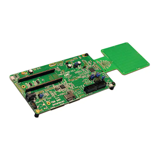
Page 6: Hardware Overview Of The Pnev7462B Board
After successful optimization, register settings can be stored in the PN7462AU EEPROM as well as saved in configuration file and used as input in design time. PN7462AU FW and SW Examples available on the product page, ranging from POS demo, contact and contactless CCID reader, P2P application, NFC forum related examples, are customized primarily for PNEV7462B/C board and supported by MCUXpresso, Keil or IAR development tools. -
Page 7: Power Circuitry
(2) USB supply, external supply & and LPC supply Fig 5. PNEV7462B supply 2.2.2 PN7462AU block The main part on the evaluation board is PN7462AU. It features a 32-bit ARM Cortex- M0-based NFC microcontroller offering a one chip solution to build contact and contactless applications. Key features are: •... -
Page 8: Lpcxpresso Block
This block provides expansion interface for LPCXpresso MCU board providing standard LPCXpresso/m-bed expansion connector (DIL54). LPCXpresso SPIM and I2CM interfaces are routed to the PN7462AU host interface selector. Additionally, board features a USB micro B connector (X1) routed to the LPC board USB interface and the LPC board reset circuit. -
Page 9: Smartcard Interface
PNEV7462B contact slot interface 2.2.5 TDA SAM extension interfaces The PN7462AU can handle more than one smart card by controlling an extra contact interface TDA8026 product from NXP. In this use case, the PN7462AU is the main controller for the electrical and protocol part for the main card slot, while the secondary slots are electrically controlled by an extra contact front-end interface (TDA), the PN7462AU being the protocol controller for these extra slots. - Page 10 UM10883 NXP Semiconductors PN7462 family Quick Start Guide - Development Kit (1) 2 optional SAM slots can be assembled Fig 8. PNEV7462B TDA8026 part schematics UM10883 All information provided in this document is subject to legal disclaimers. © NXP B.V. 2018. All rights reserved.
-
Page 11: Antenna Coil And Related Matching Circuit
UM10883 NXP Semiconductors PN7462 family Quick Start Guide - Development Kit 2.2.6 Antenna coil and related matching circuit In general, there are two antenna tunings possible with PNEV7462B board: asymmetrical symmetrical The asymmetrical tuning is the standard tuning as taken from the existing NXP NFC frontend design recommendations. - Page 12 UM10883 NXP Semiconductors PN7462 family Quick Start Guide - Development Kit Fig 9. Default 65x65 antenna matching diagram - symmetrical The antenna connection uses the standard tuning circuit Fig 10. The EMC filter is typically a second order low pass filter as shown in Fig 18, and contains an inductor (L0) and a capacitor (C0).
- Page 13 UM10883 NXP Semiconductors PN7462 family Quick Start Guide - Development Kit (1) The matching components might be adapted due to antenna layout changes. Fig 11. Antenna and matching Table 1 lists components for the “symmetric” matching. Table 1. Assembled matching components...
-
Page 14: Pcb For Individual Antenna Matching
PNEV7462B V2.2 2.3.1 PNEV7462B V2.1 The V2.1 of the customer evaluation board is the initial version of the board that comes with the launch of the PN7462AU chip. Fig 12. PNEV746B V2.1 UM10883 All information provided in this document is subject to legal disclaimers. -
Page 15: Pnev7462B V2.2
UM10883 NXP Semiconductors PN7462 family Quick Start Guide - Development Kit 2.3.2 PNEV7462B V2.2 The V2.2 of the customer evaluation board is the replacement and latest version of the customer evaluation board incl. FCC certification. Functionality of the V2.2 is the same as of V2.1. -
Page 16: Configuration Of The Pnev7462B Board
Fig 14. Board Power settings 3.1.1 PN7462AU supply options The boards offer several ways of supplying the PN7462AU IC. The main chip supply (VBUS) can be set to 5V, 3.3 V or USB supply. The corresponding setting is described in Fig 15 (1) PNEV7462B V2.1... -
Page 17: Power Supply Status Led
Fig 16. Supply indicator 3.1.3 Supply options for PVDD, VUP_TX and TVDD The PN7462AU allows different options of supplying PVDD_IN, PVDDM_IN as well as for TVDD_IN and VUP_TX. The default setting is to use the internal supply for PVDD as well as TVDD. That means default setting is PVDD_IN connected to PVDD_OUT, and TVDD_IN connected to TVDD_OUT. - Page 18 PVDD_OUT Note: If PVDD is externally supplied, the Jumper 42 (PVDD_OUT) needs to be set. By setting this Jumper the PVDD_OUT is shorted to GND and the PN7462AU turns off the PVDD LDO. UM10883 All information provided in this document is subject to legal disclaimers.
-
Page 19: Host Interface Configuration
The yellow marked jumpers (Fig 18) needs to be set for using the I2C host interface of the chip with LPCXpresso expansion board. This will connect the I²C SCL of the PN7462AU to the I/O P0 (28) and also the I²C SDA of the PN7462AU to the I/O P0(27) of the LPCXpresso board. -
Page 20: Spi Host Interface Configuration
The yellow marked jumpers (Fig 20) needs to be set for using the SPI host interface of the chip. This will connect the SPI_MOSI of the PN7462AU to the I/O P0(18), SPI_MISO to the I/O P0(17), SCK to the I/O P0(15), and also the NSS of the PN7642AU to the I/O P0(16) of the LPCXpresso board. -
Page 21: Hsuart Interface Configuration
The PNEV7462B board is equipped with a SWD interface. The SWD 10-pin Cortex connector is placed in the bottom left corner of the board. LPC-Link 2 standalone debug probe can be used to flash or debug application on the PN7462AU as illustrated on the Fig 22. -
Page 22: Hardware Overview Of The Pnev7462C Board
Fig 23. PNEV7462C board The board consists of the following blocks: 1. PN7462AU circuitry with reset and download pushbuttons and power configurations 2. External power supply connector (5.5/2.1 socket) and power supply selector 3. Power supply status LEDs for 3.3V and 5V 4. -
Page 23: Power Circuitry
Fig 24. PNEV7462C supply 4.2.2 PN7462AU block The main part on the evaluation board is PN7462AU. It features a 32-bit ARM Cortex- M0-based NFC microcontroller offering a one chip solution to build contact and contactless applications. -
Page 24: Smartcard Interface
Fig 25. PNEV7462C board schematic (PN7462AU block) 4.2.3 Smartcard interface The PN7462AU integrates contact interface to enable communication with ISO7816 and EMVCo contact smart cards, without the need for an external contact front end. It offers a high level of security for the cards by performing current limitation, short-circuit detection, ESD protection as well as supply supervision. -
Page 25: Antenna Coil And Related Matching Circuit
Symmetrical coupling is used with DPC (Dynamic Power Control) feature of the PN7462AU and offers an improved overall RF performance. This requires the antenna to be “symmetrically” tuned and it requires the AGC to correlate with the driver current ITVDD. - Page 26 UM10883 NXP Semiconductors PN7462 family Quick Start Guide - Development Kit Fig 27. Default 65x65 antenna matching diagram – symmetrical The antenna connection uses the standard tuning circuit Fig 10. The EMC filter is typically a second order low pass filter as shown in Fig 18, and contains an inductor (L0) and a capacitor (C0).
- Page 27 UM10883 NXP Semiconductors PN7462 family Quick Start Guide - Development Kit (5) The matching components might be adapted due to antenna layout changes. Fig 29. Antenna and matching Table 1 lists components for the “symmetric” matching. Table 1. Assembled matching components...
-
Page 28: Pcb For Individual Antenna Matching
UM10883 NXP Semiconductors PN7462 family Quick Start Guide - Development Kit General component Component Value Comment PNEV7462C C35/ C49 33pF C1 split in 2 parallel capacitors C37/ C47 C40/ C46 120pF C41/ C43 68pF 2,2Ω R117/ R119 split in 2 parallel resistors 2,2Ω... -
Page 29: Configuration Of The Pnev7462C
Fig 30. PNEV7462C board power source configuration 5.2 PN7462AU IC power supply options The PN7462AU IC main supply voltage input of the microcontroller (VBUS) can be configured to 5V, 3.3 V or USB, by setting theVBUS jumper as described in Fig 31 (2) VBUS 3.3V... -
Page 30: Supply Options For Pvdd, Pvdd_M, Vup_Tx
NXP Semiconductors PN7462 family Quick Start Guide - Development Kit Fig 32. Power supply status LEDs 5.4 Supply options for PVDD, PVDD_M, VUP_TX and TVDD The PN7462AU allows different options of supplying: • PVDD_IN (pad supply voltage input) • PVDD_M_IN (pad supply voltage input for master interfaces) •... -
Page 31: Host Interfaces
Internal TX LDO is activated by software and corresponding setting is in EEPROM configuration. Fig 33. Default power supply setting 5.5 Host interfaces The PN7462AU supports interfacing one out of the four different host at the time: • USB 2.0 full speed with USB 3.0 hub connection capability, •... -
Page 32: Debug Interface
UM10883 NXP Semiconductors PN7462 family Quick Start Guide - Development Kit 5.6 Debug interface The PNEV7462C board has SWD interface port (JP4 10-pin Cortex connector). The LPC-Link 2 standalone debug probe connects to this interface via flat cable from J7 as illustrated on the following picture. -
Page 33: Nfc Cockpit Getting Started
“<installation directory>\firmware\PN7462AU”. Additionally, appropriate EEPROM settings needs to be updated, the EEPROM settings binary is located in “<installation directory>\firmware\PN7462AU”. The EEPROM binary is also updated by using primary downloader functionality (see chapter 8.10). USB drivers needed for NFC Cockpit are part of the installation package and are automatically installed. - Page 34 UM10883 NXP Semiconductors PN7462 family Quick Start Guide - Development Kit (4) click <Activate Layer4> button (5) enter 6A and press <Send Data> The PN7462 NFC Cockpit shows the card responses like ATQA, SAK, and ATS. Afterwards the ISO/IEC 14443-4 protocol can be used to exchange data. Once the MIFARE DESFire command “Get Application ID”...
-
Page 35: Pn7462 Family Register Access
Selecting a register reads and shows the hexadecimal value as well as the corresponding bit values. The input allows to change each bit separately as well as writing hexadecimal values. Writing back the value changes the PN7462AU register. On “mouse over”, the application displays a short description of the register parts. -
Page 36: Pn7462 Family Ic Internal Test Bus
UM10883 NXP Semiconductors PN7462 family Quick Start Guide - Development Kit • Write EEPROM - writes a single byte into EEPROM using byte address • Dump EEPROM - stores the complete user area of the PN7462 family IC EEPROM into a binary file. This can be used to generate a backup of all settings or to transfer optimized settings onto another board or into own software. -
Page 37: Pn7462 Family Dynamic Power Control
UM10883 NXP Semiconductors PN7462 family Quick Start Guide - Development Kit Fig 38. PN7462 family IC analog and digital test signals The analog test signals can be directly selected at GPIO1 and 2. For the digital test signals GPIO4 and 5 can be used. -
Page 38: Pn7462 Family Adaptive Wave Control
UM10883 NXP Semiconductors PN7462 family Quick Start Guide - Development Kit Fig 39. PN7462 family IC DPC 6.9 PN7462 family Adaptive Wave Control The PN7462 family IC DPC functionality offers the option to use a lookup table to dynamically control the TX shaping. This feature is called Adaptive Wave Control (AWC). -
Page 39: Proposal For "Static" Tx Shaping Adjustment
UM10883 NXP Semiconductors PN7462 family Quick Start Guide - Development Kit (1) Example: Running in an endless loop for Type A @ 106 settings Fig 40. PN7462 family IC AWC 6.9.1 Proposal for “static” Tx shaping adjustment Step1: Save EEPROM for backup (<Dump EEPROM>), then disable the AWC (<Disable AWC>). -
Page 40: Proposal For "Dynamic" Tx Shaping Adjustment
UM10883 NXP Semiconductors PN7462 family Quick Start Guide - Development Kit 6.9.2 Proposal for “dynamic” Tx shaping adjustment Requirement: “static” TX shaping adjustment is done properly. Step1: Save EEPROM for backup (<Dump EEPROM>), then disable the AWC (<Disable AWC>), if not done before. -
Page 41: Rx Matrix Test Principle
UM10883 NXP Semiconductors PN7462 family Quick Start Guide - Development Kit one parameter might require another parameter to change, too. At the end, even several “optima” might occur, which show similar performance. There might be external influence like noise (e.g. from an LCD or other electronic circuitry) resulting in a different optimum. -
Page 42: Rx Matrix Xml Input File
UM10883 NXP Semiconductors PN7462 family Quick Start Guide - Development Kit Of course, the real smart card does not allow to vary the load modulation level, which helps to find the optimum (sensitivity). So, an extended test setup as shown in Fig 42 can be used to control the LMA voltage level. - Page 43 UM10883 NXP Semiconductors PN7462 family Quick Start Guide - Development Kit Parameter Meaning Example value protocolType Defines the used protocol and bit rate RM_A_106 Table 4. Send Data input Parameter Meaning Example value shortFrame Enables a short frame (e.g. for REQA)
-
Page 44: Nfc Cockpit With Awg
UM10883 NXP Semiconductors PN7462 family Quick Start Guide - Development Kit 6.11 NFC Cockpit with AWG 6.11.1 NI VISA installation The NFC Cockpit supports the control of a Keysight AWG (see [13]) via USB. As a prerequisite, the USB driver and National Instruments VISA driver package [14] have to be installed. - Page 45 UM10883 NXP Semiconductors PN7462 family Quick Start Guide - Development Kit (1) ATQA response for TX_IRQ as trigger Fig 44. AWG setup for type A @ 106 The amplitude defines the peak voltage level of the LMA: the LMA output toggles between 0V and the defined amplitude.
-
Page 46: Awg Setup And Test For Type B @ 106
UM10883 NXP Semiconductors PN7462 family Quick Start Guide - Development Kit The trigger delay defines the delay between AWG trigger input and the LMA sequence start. The given 80µs define a standard FDT for type A, if the TX_IRQ signal is taken as trigger signal. - Page 47 UM10883 NXP Semiconductors PN7462 family Quick Start Guide - Development Kit (2) ATB response 0x50AEF9ACD3058901013381E1 with TX_IRQ as trigger. Fig 45. AWG setup for type B @ 106 The amplitude defines the peak voltage level of the LMA: the LMA output toggles between 0V and the defined amplitude.
-
Page 48: Rx Matrix Test With Awg
UM10883 NXP Semiconductors PN7462 family Quick Start Guide - Development Kit The trigger delay defines the delay between AWG trigger input and the LMA sequence start. The given 300µs define a standard TR0 for type B, if the TX_IRQ signal is taken as trigger signal. -
Page 49: Pn7462 Family Low Power Card Detection
UM10883 NXP Semiconductors PN7462 family Quick Start Guide - Development Kit The Fig 47 shows the result of such a test run to indicate the sensitivity limit with RxGain = 2, HPCF = 2, MinLevel = 3 and MinLevel = 6. -
Page 50: Secondary Fw - Emvco Loopback Application
UM10883 NXP Semiconductors PN7462 family Quick Start Guide - Development Kit 6.13 Secondary FW - EMVCo Loopback application The FW might contain additional applications (see 6.3), which can then be started via the Secondary FW tab. The default Secondary FW application is: EMVCo Loopback: Test application for EMVCo L1 certification The EMVco Loopback (or other application) can be started by pressing the <Start... -
Page 51: Software Application Stack
UM10883 NXP Semiconductors PN7462 family Quick Start Guide - Development Kit 7. Software application stack The PN7462 family firmware is a modular software written in C language, which provides an API that enables customers to create their own contact and contactless software stack and applications for the PN7462 Family [5]. -
Page 52: Hardware Abstraction Layer - Hal
UM10883 NXP Semiconductors PN7462 family Quick Start Guide - Development Kit Fig 51. Architecture diagram 7.1 Hardware abstraction layer – HAL Hardware abstraction layer – HAL is responsible for the CPU, communication, memory and utility peripherals. HAL composed of a set of HW functions, HW ISR and OSAL functions. -
Page 53: Application Layer - Al
UM10883 NXP Semiconductors PN7462 family Quick Start Guide - Development Kit • ISO14443-3B: Contactless proximity card air interface communication at 13.56MHz for the Type B contactless cards. • ISO14443-4: Specifies a half-duplex block transmission protocol featuring the special needs of a contactless environment and defines the activation and deactivation sequence of the protocol. -
Page 54: Component View
UM10883 NXP Semiconductors PN7462 family Quick Start Guide - Development Kit 7.5 Component view 7.5.1 Contactless component view In contactless component view (Fig 52) for the “phExMain” example is shown. Fig 52. Contactless architecture view UM10883 All information provided in this document is subject to legal disclaimers. -
Page 55: Contact Component View
UM10883 NXP Semiconductors PN7462 family Quick Start Guide - Development Kit 7.5.2 Contact component view In the Fig 53 contact component view for the “phExMain” example is shown. Fig 53. Contact architecture view 7.6 Building a project from bottom to top In order to use the PN7462 family firmware, a stack of components has to be initialized from bottom to top. -
Page 56: Rtos And It´s Usage
The Flash boot performs the boot reason handling and initialization of common HALs. See Below are the lists of examples available in current release to demonstrate the HW and FW features of PN7462AU IC. In general, the FreeRTOS Scheduler has 2 default tasks running which are Idle task and Timer task whose priority is kept lower than the application tasks. -
Page 57: Managing The Pn7462 Family Sw Projects With Mcuxpresso Ide
Fig 56 gives general overview of the development environment elements and their interconnections: Fig 56. Overview of PN7462AU development environment UM10883 All information provided in this document is subject to legal disclaimers. © NXP B.V. 2018. All rights reserved. -
Page 58: Installation Of The Mcuxpresso Ide
UM10883 NXP Semiconductors PN7462 family Quick Start Guide - Development Kit 8.2 Installation of the MCUXpresso IDE The MCUXpresso IDE enables powerful application development for NXP MCUs based on ARM® Cortex®-M cores, including LPC and Kinetis microcontrollers. The MCUXpresso IDE offers advanced editing, compiling and debugging features with the addition of MCU-specific debugging views, code trace and profiling, multicore debugging, and more. -
Page 59: Installing Pn7462Au Fw And Sw Examples Package
Semiconductors\PN7462AUPspPackageFull-vXX_XX_XX\PN7462AU Software folder. 8.4 Updating PN7462AU EEPROM configuration Before running or debugging the example applications, the PN7462AU needs to be updated with the latest EEPROM configuration. EEPROM update is described in the chapter 8.8. The EEPROM configuration file is located in the \PN7462AU\phHal\phCfg\user_ee.bin file. -
Page 60: Importing Provided Sw Example Projects
UM10883 NXP Semiconductors PN7462 family Quick Start Guide - Development Kit 8.5 Importing provided SW example projects The use of Quickstart Panel provides fast access to the most commonly used features of the MCUXpresso IDE. Quickstart Panel easies importing, creating, building and debugging projects. - Page 61 NXP Semiconductors PN7462 family Quick Start Guide - Development Kit Fig 61. Importing project to MCUXpresso IDE (2) Browse to the PN7462AU-FW_vXX.XX.XX_Full.zip” and click “Next”. UM10883 All information provided in this document is subject to legal disclaimers. © NXP B.V. 2018. All rights reserved.
- Page 62 UM10883 NXP Semiconductors PN7462 family Quick Start Guide - Development Kit Fig 62. Select project Select projects to be imported and then click “Finish”. Selected examples will be imported to the workspace. When the import process is finished, the development and editing the code can start.
-
Page 63: Building Projects
UM10883 NXP Semiconductors PN7462 family Quick Start Guide - Development Kit Fig 63. Project Workspace with all examples 8.6 Building projects Building projects in a workspace can be started trough Quickstart Panel - ‘Build all projects’ command. Alternatively, a single project can be selected in the “Project Explorer View”... - Page 64 As a part of the build process, the binary file for flash in AXF format is created. This binary file can be used to update PN7462AU flash via USB mass storage interface or by using flash tool or debug in MCUXpresso IDE. In case that “Binaries” folder is not visible in the project structure, refresh the project (right click on project and select “Refresh”).
-
Page 65: Running And Debugging The Example Projects
8.7 Running and debugging the example projects This description shows how to run the PN7462AU “PN7462AU_ex_phExMain” example application for the PN7462AU customer development board in debug mode. The same basic principles will apply for all other examples. In cases where example will need additional configuration this will be detailed described in the example description. - Page 66 (), the application is started (by simulating a processor reset), and code is executed until the default breakpoint is hit. To start debugging your application on the PN7462AU, simply highlight the project in the Project Explorer and then in the Quick start Panel click Debug, as shown in Fig 68. The MCUXpresso IDE will first build application and then start debugging.
- Page 67 UM10883 NXP Semiconductors PN7462 family Quick Start Guide - Development Kit Fig 68. Launch debug session Fig 69. Selecting debug probe UM10883 All information provided in this document is subject to legal disclaimers. © NXP B.V. 2018. All rights reserved.
- Page 68 UM10883 NXP Semiconductors PN7462 family Quick Start Guide - Development Kit Fig 70. Project debugging After the software upload, the execution of the application starts immediately. UM10883 All information provided in this document is subject to legal disclaimers. © NXP B.V. 2018. All rights reserved.
-
Page 69: Break Points
PN7462 family Quick Start Guide - Development Kit 8.7.1 Break points PN7462AU supports 4 breakpoints and 2 watch points. In usual way, double click on the left vertical editor strip to set the break points. The execution of the application will be stopped when the break point is reached. -
Page 70: Debug Traces
UM10883 NXP Semiconductors PN7462 family Quick Start Guide - Development Kit 8.7.2 Debug traces The debug traces can be seen on console as shown in Fig 72. Fig 72. Debug view and debugger traces UM10883 All information provided in this document is subject to legal disclaimers. -
Page 71: Peripheral View
PN7462 family Quick Start Guide - Development Kit 8.7.3 Peripheral view MCUXpresso IDE provides direct access to all the peripheral registers of the PN7462AU. To see the peripheral registers, follow the steps as shown below. (1) Go to Window Show view Other (2) Select “Peripherals+”... - Page 72 PN7462 family Quick Start Guide - Development Kit (1) Select the relevant peripheral (2) Register, bit fields and description in the relevant view Fig 74. PN7462AU EECTRL peripheral view UM10883 All information provided in this document is subject to legal disclaimers.
-
Page 73: Updating Pnev7462B/C Board Firmware (Flash And Eeprom Memory)
PN7462 family Quick Start Guide - Development Kit 8.8 Updating PNEV7462B/C board firmware (flash and EEPROM memory) PN7462AU flash memory can be updated either by using SWD interface and LPC-Link 2 debug probe or from primary bootloader mode (USB MSD). - Page 74 UM10883 NXP Semiconductors PN7462 family Quick Start Guide - Development Kit (1) Select conection script, flash driver and binary file (2) Ensure that all the options are set properly and click OK Fig 77. Build output - flash binary file After selecting binary file flash process starts, and report is shown.
-
Page 75: Updating Flash And Eeprom Via Usb Msd Interface
Fig 79. PN7462AU as USB mass storage device Now the PNEV7462B is detected by the PC as an USB MSD. Fig 80. PN7462AU IC detected as USB mass storage device for flash/ EEPROM upgrade UM10883 All information provided in this document is subject to legal disclaimers. - Page 76 UM10883 NXP Semiconductors PN7462 family Quick Start Guide - Development Kit When the PN7462AU is mounted as a USB mass storage device, the files listed in the table below are visible in the device root. Table 7. Files found in USB mass storage...
-
Page 77: Pn7462Au Software Examples
UM10883 NXP Semiconductors PN7462 family Quick Start Guide - Development Kit PN7462AU software examples 9.1 General overview For a detailed description of examples, please refer to the [5]. Before running examples assure the proper EEPROM configuration is updated (see 8.4). -
Page 78: Pn7462Au_Ex_Phexmain - (Clif + Ctif Functionality)
UM10883 NXP Semiconductors PN7462 family Quick Start Guide - Development Kit 9.2 PN7462AU_ex_phExMain – (CLIF + CTIF functionality) The “phExMain” is the main example demonstrating CLIF and CTIF functionalities. CLIF functionality covering NFC Forum operation modes: R/W mode, card mode and P2P mode. -
Page 79: Features
UM10883 NXP Semiconductors PN7462 family Quick Start Guide - Development Kit External power supply LPC-LIN K2 Fig 82. HW setup for the main example 9.2.2 Features “phExMain” example is covering the following features: Table 10. “phExMain” Example features Feature supported... -
Page 80: Operation With Standby And Without Standby
UM10883 NXP Semiconductors PN7462 family Quick Start Guide - Development Kit • CLIF Task which executes NFC A, B, F reader application or EMV application and discovery loop • CT Task which does an activation of a JCOP contact card, selects the T=1 protocol and executes EMV Card application. - Page 81 UM10883 NXP Semiconductors PN7462 family Quick Start Guide - Development Kit Fig 83. phExMain standby flow UM10883 All information provided in this document is subject to legal disclaimers. © NXP B.V. 2018. All rights reserved. User manual Rev. 1.6 — 14 May 2018...
-
Page 82: Mifare Classic
UM10883 NXP Semiconductors PN7462 family Quick Start Guide - Development Kit Fig 84. phExMain non standby flow 9.2.5 MIFARE Classic The MIFARE Classic example is implementing basic read/write functionality using a MIFARE Classic card with a predefined default key. If a Type A card is detected with SAK of 0x8 (1K MIFARE Classic card) or 0x18 (4K MIFARE Classic card), then the MIFARE Classic example is executed. -
Page 83: Mifare Ultralight
UM10883 NXP Semiconductors PN7462 family Quick Start Guide - Development Kit 9.2.6 MIFARE Ultralight The MIFARE Ultralight example is implementing basic read/write functionality using a non-secure MIFARE Ultralight card. If a Type A card is detected with SAK 0x00, then MIFARE Ultralight example is executed. -
Page 84: Iso18000-3.3 - Icode Ilt
UM10883 NXP Semiconductors PN7462 family Quick Start Guide - Development Kit 2. Write single block 3. Datarate Tx - 26kbit/s (1out of 4 coding) and Rx 26kbit/s Implementation in the “phExMain_ISO15693.c” file. 9.2.10 ISO18000-3.3 – ICODE ILT The example performs read and write to predefined blocks of the card. -
Page 85: Passive And Active Iso18092 Initiator (Till Activation)
UM10883 NXP Semiconductors PN7462 family Quick Start Guide - Development Kit does not demonstrate L4 APDUs exchange (it is done in phExHCE and phExNFCForum). 9.2.14 Passive and active ISO18092 initiator (till activation) During active poll mode, if ATR_REQ is received or during passive poll mode, if SAK denotes 0x40, then the example implemented in phExMain_PasIni.c/ phExMain_ActIni.c... - Page 86 UM10883 NXP Semiconductors PN7462 family Quick Start Guide - Development Kit c. Waits for PMU/PCR exception events d. Waits for CLIF Task completion if standby is enabled e. Waits for CT Task completion if standby is enabled f. Enter low power mode (standby) 2.
- Page 87 UM10883 NXP Semiconductors PN7462 family Quick Start Guide - Development Kit Fig 85. PN7462AU phExMain sequence diagram for standby scenario with RTOS UM10883 All information provided in this document is subject to legal disclaimers. © NXP B.V. 2018. All rights reserved.
-
Page 88: No-Rtos Management
UM10883 NXP Semiconductors PN7462 family Quick Start Guide - Development Kit Fig 86. PN7462AU phExMain sequence diagram for non-standby scenario with RTOS 9.2.18 No-RTOS management In case of No-RTOS the entry point from flash boot is phExMain_NoRTOS. The functionality remains the same except that the CLIF example and the CT examples are called from a single executive while loop based on timer interrupt or external RF detection or CT presence interrupt. -
Page 89: Pn7462Au_Ex_Phexemvco (Clif + Ctif Functionality)
UM10883 NXP Semiconductors PN7462 family Quick Start Guide - Development Kit 9.3 PN7462AU_ex_phExEMVCo (CLIF + CTIF functionality) The “phExEMVCo” is an example which implements the polling for the EMVCo contact and contactless cards and implement reference EMV transaction. Application is based on the NFC Reader Library, CT Library and be run with or without FreeRTOS. -
Page 90: Emvco Polling Loop
UM10883 NXP Semiconductors PN7462 family Quick Start Guide - Development Kit Feature supported Non RTOS Standby mode HIF/MIF Interface 9.3.3 EMVCo polling loop In this example EMVCo polling loop is enabled. In this profile, only Type A and B technology polling is enabled and bail out is set such that both A and B techs are polled even if one of them is detected. -
Page 91: Pn7462Au_Ex_Phexrf (Cl Functionality)
UM10883 NXP Semiconductors PN7462 family Quick Start Guide - Development Kit 9.4 PN7462AU_ex_phExRf (CL functionality) The “phExRf” is an example which implements the polling for contactless cards without NFC Reader Library support. Application use only HAL APIs and perform same CLIF functionality as 0 “phExMain”... -
Page 92: Application Flow
UM10883 NXP Semiconductors PN7462 family Quick Start Guide - Development Kit Feature supported NXP NFC Reader Library CT Reader Library FreeRTOS Non RTOS Standby mode HIF/MIF Interface 9.4.3 Application Flow The figure below demonstrates the application flow. Fig 89. phExRF Example Application Flow UM10883 All information provided in this document is subject to legal disclaimers. -
Page 93: Pn7462Au_Ex_Phexrfpoll Example (Cl Functionality)
UM10883 NXP Semiconductors PN7462 family Quick Start Guide - Development Kit 9.5 PN7462AU_ex_phExRFPoll example (CL functionality) The “phExRfPoll” is an example which implements the polling for contactless cards without NFC Reader Library support for the optimization of the RF-signal. Through defines in phExRfPoll.c the specific technology to poll for can be selected. -
Page 94: Features
UM10883 NXP Semiconductors PN7462 family Quick Start Guide - Development Kit 9.6.2 Features phExCT” example is covering next features: Table 13. “phExRf” Example features Feature supported CLIF Interface CT Interface NXP NFC Reader Library CT Pal Library FreeRTOS Non RTOS... -
Page 95: Emvco Activation
UM10883 NXP Semiconductors PN7462 family Quick Start Guide - Development Kit Fig 91. phExCT Example Application Flow 9.6.4 EMVCo activation The example performs EMVCo activation and EMVCo ATR parsing. It also determines the protocol supported by the card. 9.6.5 SELECT master card The example sends a SELECT master card APDU and expects a RAPDU 0x90 0x00. -
Page 96: Pn7462Au_Ex_Phexctemvco (Ct Functionality)
UM10883 NXP Semiconductors PN7462 family Quick Start Guide - Development Kit 9.7 PN7462AU_ex_phExCTEMVCo (CT functionality) The “phExCtEMVCo” is an example which implements the CT functionality with CT Pal library support. Application use CT PAL library APIs and perform same CT functionality as 0 “phExEMVCo”... -
Page 97: Pn7462Au_Ex_ Phexct7816 (Ct Functionality)
UM10883 NXP Semiconductors PN7462 family Quick Start Guide - Development Kit 9.8 PN7462AU_ex_ phExCT7816 (CT functionality) The “PN7462AU_ex_phExCt7816” example implements the CT functionality with CT library support. Application use CT library APIs and perform same CT functionality as in “PN7462AU_ex_phExMain” example with the only difference that for the transaction static predefined packets are used. -
Page 98: Pn7462Au_Ex_Phexhif
Application is implementing CT functionality with SPI Host interface and it is not based on the FreeRTOS. Setup consist of two projects: HIF application executing on the PN7462AU and the LPC application executing on the LPC1769 board (LPCXpresso board for LPC1769 with CMSIS DAP probe [9]). - Page 99 PN7462 family Quick Start Guide - Development Kit Fig 92. HIF demo architecture The GPIOs of LPC and PN7462AU are used to determine which functionality of this example has to be executed (GPIO6,7,8). It is also used to select the host interface or master interface to be used (GPIO4,5).
-
Page 100: Features
UM10883 NXP Semiconductors PN7462 family Quick Start Guide - Development Kit (1) IRQ line VIA marked yellow (2) An additional wire should be solder on this VIA to make the IRQ line accessible Fig 93. PNEV7462C IRQ pin 9.9.2 Features “phExHif”... -
Page 101: Hif Selection
• 0 Logical HIGH as seen/set by the GPIO. • Start PN7462AU Application before launching LPC Application • Since both the projects are MCUXpresso IDE based, while updating FW image via the LPC Link, ensure that the image is downloaded to the correct platform. - Page 102 UM10883 NXP Semiconductors PN7462 family Quick Start Guide - Development Kit • Boot: EEPROM • Boot: FLASH • Boot: CT • Boot: GPIO • HW: I2CM • HW: SPIM • HW: HIF UM10883 All information provided in this document is subject to legal disclaimers.
-
Page 103: Mcuxpresso Projects Provided For Lpc1769
Fig 94. POS use case demo architecture The POS demo architecture is split into application layer (L2) and low level EMVCo compliant layer L1 which is hosted on the PN7462AU. The application layer L2 commands are simulated in reference microcontroller board (LPC1769) and L1 layer components are placed in PN7462AU. -
Page 104: Pn7462Au_Ex_Phexccid
CCID reader and shows how connected PN7462AU via USB interface to a PC and provide the CCID protocol implementation on the top of the physical link. The PC USB reader example is hosted on the PN7462AU and can be tested with any PC/SC application running on the PC with Windows OS. -
Page 105: Pn7462Au_Ex_Phsystemservices
PN7462 family Quick Start Guide - Development Kit Fig 96. PC USB reader example block diagram The USB stack and CCID class is implemented in the PN7462AU. The default CCID driver present in PC with Windows OS is used for operation. - Page 106 Block SWD debugging This command disables PN7462AU SWD debug interface. When the PN7462AU IC is delivered from production to user, the default SWD access level enables the user to view and debug user flash memory, user EEPROM memory, user RAM memory, and peripheral registers.
-
Page 107: Pn7462Au_Ex_Phexvcom
UM10883 NXP Semiconductors PN7462 family Quick Start Guide - Development Kit Note: For irreversible commands: Secrow lock, code write protection, block SWD debugging and disable primary download the undo is not possible! 9.13 PN7462AU_ex_phExVCom This example application features TypeA card detection, RF filed control and communication with the PC host over USB CDC interface (VCOM). -
Page 108: Pn7462Au_Ex_Phexdooraccessec
UM10883 NXP Semiconductors PN7462 family Quick Start Guide - Development Kit available. In case the NFC device is detected, the application sends a NDEF message containing the NXP webpage address. PN7462AU NFC Reader Fig 98. Door access example After each polling loop the application goes to standby mode and remains for 500ms. A timer is used as a wakeup source from standby. -
Page 109: Pn7462Au_Ex_Phexnfcccid
UM10883 NXP Semiconductors PN7462 family Quick Start Guide - Development Kit MIFARE PN7462AU SAM AV2 NFC Reader Fig 99. Door Access Example - Export Controlled Version On power-up, NFC Reader starts polling for (PICC) cards (Type A, B or F, ISO15693, ISO18000-3M3) and if no card is present, the reader goes to standby mode. -
Page 110: Pn7462Au_Ex_Phexrfpcda
UM10883 NXP Semiconductors PN7462 family Quick Start Guide - Development Kit 2. AES authentication of the application. 3. Changing of the key. 4. Enciphered Read of Value File and Plain Read of Data File. 5. Enciphered Write of Value File and Plain write of Data File. -
Page 111: Abbreviations
UM10883 NXP Semiconductors PN7462 family Quick Start Guide - Development Kit 10. Abbreviations Table 19. Abbreviations Acronym Description APDU Application Protocol Data Unit Application Programming Interface CLIF Contactless Interface Cyclic Redundancy Code CTIF Contact Interface EEPROM Electrically Erasable Programmable Read Only Memory... -
Page 112: Annex A Rx Matrix Xml Input File Examples
11.1 Type A example without AWG control <?xml version="1.0" encoding="UTF-8" standalone="no" ?> <!DOCTYPE Test SYSTEM "NNC_RxMatrix_Pn7462AU.dtd"> <!-- This is an example of a TypeA test script for Pn7462AU where we acess bit fields of regsiters in a range--> <Test numberMaxOfPasses="10"... -
Page 113: References
UM10883 NXP Semiconductors PN7462 family Quick Start Guide - Development Kit 12. References OM27462CDK NFC controller development kit https://www.nxp.com/products/:OM27462CDK Om27462CDKP NFC controller development kit https://www.nxp.com/products/:OM27462CDKP PN7462 family Datasheet https://www.nxp.com/docs/en/data-sheet/PN7462.pdf MCUXpresso webpage http://mcuxpresso.nxp.com/ PN7462 family Software User’s Manual https://www.nxp.com/docs/en/user- guide/UM10913.pdf NFC-COCKPIT: NFC Cockpit configuration tool for NFC ICs http://www.nxp.com/products/:NFC-COCKPIT... -
Page 114: Legal Information
This document supersedes and replaces all information supplied prior to the publication hereof. Purchase of an NXP Semiconductors IC that complies with one of the Near Field Communication (NFC) standards ISO/IEC 18092 and ISO/IEC 21481 Suitability for use — NXP Semiconductors products are not designed,... -
Page 115: List Of Figures
Fig 16. Supply indicator ..........17 Fig 52. Contactless architecture view ......54 Fig 17. Default supply connection of the PN7462AU using all blocks ..........18 Fig 53. Contact architecture view ........ 55 Fig 18. Host Interface selection – USB mode ..... 19 Fig 54. - Page 116 Build output - flash binary file ......74 Fig 78. Program flash report ........74 Fig 79. PN7462AU as USB mass storage device ..75 Fig 80. PN7462AU IC detected as USB mass storage device for flash/ EEPROM upgrade ....75 Fig 81.
-
Page 117: List Of Tables
UM10883 NXP Semiconductors PN7462 family Quick Start Guide - Development Kit 15. List of tables Table 1. Assembled matching components ....13 Table 2. Supply options ..........18 Table 3. PN7462 HIF pins ..........19 Table 1. Assembled matching components ....27 Table 3. -
Page 118: Table Of Contents
Configuration of the PNEV7462C ..... 29 PNEV7462C Board power settings ....29 Hardware overview of the PNEV7462B board ... 6 PN7462AU IC power supply options ....29 PNEV7462B concept ......... 6 Power supply status LEDs ........ 29 PNEV7462B board ..........6 Supply options for PVDD, PVDD_M, VUP_TX 2.2.1... - Page 119 No-RTOS management ........88 Development environment ....... 57 PN7462AU_ex_phExEMVCo (CLIF + CTIF Installation of the MCUXpresso IDE ....58 functionality) ............. 89 Installing PN7462AU FW and SW examples 9.3.1 Demo setup ............89 package ............59 9.3.2 Features ............89 Updating PN7462AU EEPROM configuration ..
- Page 120 UM10883 NXP Semiconductors PN7462 family Quick Start Guide - Development Kit 9.7.4 APDU transactions ........... 96 PN7462AU_ex_ phExCT7816 (CT functionality) ................. 97 9.8.1 Demo setup ............97 9.8.2 Features ............97 9.8.3 ISO7816 activation ........... 97 9.8.4 APDU transactions ........... 97 PN7462AU_ex_phExHif ........
- Page 121 Mouser Electronics Authorized Distributor Click to View Pricing, Inventory, Delivery & Lifecycle Information: OM27462CDKM...
Need help?
Do you have a question about the PN7462AU and is the answer not in the manual?
Questions and answers