Table of Contents
Advertisement
Quick Links
Freescale Semiconductor
User Guide
APPLICATION MODULE STUDENT LEARNING
KIT FEATURING FREESCALE MC9S12DT256
© Freescale Semiconductor, Inc., 2006. All rights reserved.
_______________________________________________________________________
For use with the following part numbers:
CSM12D with MC9S12DT256 chipset
SLKS12DT256UG
Rev. 1, 9/2007
APS12DT256SLK
PBS12DT256SLK
Advertisement
Table of Contents

Subscribe to Our Youtube Channel
Related Manuals for NXP Semiconductors freescale semiconductor CSM12D


Summary of Contents for NXP Semiconductors freescale semiconductor CSM12D
- Page 1 Freescale Semiconductor SLKS12DT256UG User Guide Rev. 1, 9/2007 APPLICATION MODULE STUDENT LEARNING KIT FEATURING FREESCALE MC9S12DT256 For use with the following part numbers: CSM12D with MC9S12DT256 chipset APS12DT256SLK PBS12DT256SLK © Freescale Semiconductor, Inc., 2006. All rights reserved. _______________________________________________________________________...
-
Page 2: Table Of Contents
CONTENTS CAUTIONARY NOTES ......................4 TERMINOLOGY.........................4 FEATURES ..........................5 REFERENCES ...........................5 REFERENCES ...........................6 GETTING STARTED........................7 OPERATING MODES ........................7 RUN MODE ........................... 7 DEBUG MODE ........................8 DEVELOPMENT SUPPORT ......................9 SOFTWARE DEVELOPMENT ....................9 MEMORY MAP........................9 BDM_PORT HEADER......................10 EXPANDED MODE OPERATION ..................10 MODE.......................... - Page 3 TABLE OF FIGURES Figure 1: BDM_PORT.......................10 Figure 2: MODE Option Header ....................10 Figure 3: PWR_SEL Option Header ..................11 Figure 4: COM_EN Header ......................13 Figure 5: COM Connector......................13 Figure 6. CAN_PORT Connector ....................14 Figure 7: Connector J1 ......................17 TABLE OF TABLES Table 1: DT256 Memory Map .....................9 Table 2: COM Connections ......................12 Table 3: ATD Reference Voltage....................14...
-
Page 4: Cautionary Notes
CAUTIONARY NOTES 1) Electrostatic Discharge (ESD) prevention measures should be used when handling this product. ESD damage is not a warranty repair item. 2) Axiom Manufacturing does not assume any liability arising out of the application or use of any product or circuit described herein; neither does it convey any license under patent rights or the rights of others. -
Page 5: Features
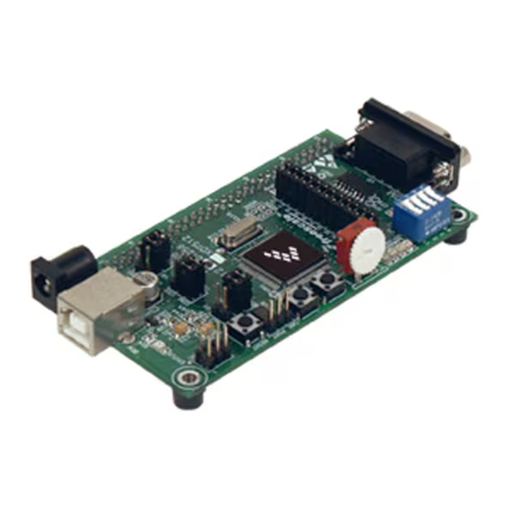
FEATURES The APS12DT256SLK is an educational development module supporting the Freescale MC9S12DT256 microcontroller (MCU). Application module SLK’s include components for out- of-box operation and are preprogrammed with a serial monitor to make application development quick and easy. A background DEBUG port is provided for development tool use and is compatible with HCS12 BDM interface cables and software. -
Page 6: References
REFERENCES The latest product information, updates and reference documents can be found at www.freescale.com and/or www.axman.com SLKS12DT256UG.pdf APS12DT256SLK User Guide (this document) APS12DT256SLKSCHEM.pdf APS12DT256SLK Schematic 9S12DT256_ZIP.zip MC9S12DT256 Device User Guide APS12DT256PG.pdf Quick Start Guide for stand alone module operation APS12DT256_DEMO.zip CodeWarrior Project to support APS12DT256PG The following reference documents are available online for using the application module in conjunction with the Freescale Microcontroller Project Board Student Learning Kit:... -
Page 7: Getting Started
GETTING STARTED Please refer to the APS12DT256SLK Quick Start Users Guide to quickly setup the stand-alone application module or PBS12DT256SLK Quick Start Users Guide to get started with the microcontroller project board (PBMCUSLK). OPERATING MODES The APS12DT256SLK board operates in two operating modes: Run Mode, or Debug Mode. Run Mode allows user application code to execute from Power-On or Reset. -
Page 8: Debug Mode
DEBUG MODE Debug Mode supports application development and debug. Debug mode is available to the user through the factory loaded serial monitor, integrated USB-BDM on the PBMCUSLK or an external HC(S)12 BDM cable. Refer to the PBMCUSLK User Guide for details on using the integrated USB-BDM. -
Page 9: Development Support
DEVELOPMENT SUPPORT SOFTWARE DEVELOPMENT Software development will require the use of an HC(S)12 assembler or compiler and a host PC operating a debug interface. Supplied with this board is the CodeWarrior Development Studio along with the Axiom IDE for Windows for debugging and flash programming. MEMORY MAP The APS12DT256SLK is designed to support the MC9S12D family of MCU’s specifically the MC9S12DT256. -
Page 10: Bdm_Port Header
BDM_PORT HEADER A 6-pin BDM port header allows connection of a HC(S)12 compatible BDM cable for application development. Refer to the BDM cable documentation for details on use of the BDM cable with this module. Figure 1: BDM_PORT MODC/BKGD 1 2 GND See the HC12 Reference Manual for complete DEBUG documentation... -
Page 11: Power Select
The on-board voltage regulator (VR1) accepts power input through a 2.1mm barrel connector (PWR). Input voltage may range from +7V to +18V. The voltage regulator (VR1) provides a +5V fixed output voltage with current output limited to 250mA. Over-temperature and over- current limit built into the voltage regulator provides protection from excessive stresses. -
Page 12: Low Voltage Reset
Low Voltage RESET A DS1813, low-voltage supervisor at LV1 protects the APS12DT256SLK under-voltage conditions. LV1 will assert RESET when the 5V rail falls below the trip point of 4.62V. LV1 will assert RESET for approximately 150ms after voltage returns to nominal. TIMING Timing input to the MCU is provided by a 4 MHz, fundamental frequency, crystal oscillator. -
Page 13: Com Connector
Communications signals Tx/Rx route to connector J1 for use off-module if desired. When using these signal to drive off-module RS-232 devices or when attempting alternate communications protocols such at IrDA or LIN, the user should disconnect the on-board RS- 232 transceiver. The COM_EN header block allows the user to selectively disable each of the 4 communications signals. -
Page 14: Mscan
MSCAN The APS12DT256SLK provides one PCA82C250 high-speed CAN physical interface. A 3-pin connector provides connectivity to the off-board CAN bus. The CAN PHY connects to the CAN0 channel on the MCU. The PHY supports data rates up to 1 Mbps with slew-rate control. The figure below shows the pin-out of the CAN_PORT connector. -
Page 15: User I/O
USER I/O User I/O includes 2 push button switches, one 4-position DIP switch, 4 green LEDs, a potentiometer, and a photo-sensor. The sections below provide details on each User I/O. The User option header block enables or disables each User I/O individually. Switches The APS12DT256SLK target board provides 2 push button switches and one 4-position DIP switch for user input. -
Page 16: Signals
Signals The following table shows the connections for each user I/O device. Table 4: User I/O USER Ref Des Signal Device PP0/KWP0/PWM0/MISO1 Push Button Switch PP1/KWP1/PWM1/MOSI1 Push Button Switch SW3-1 PB0/ADDR0/DATA0 4-pos DIP Switch SW3-2 PB1/ADDR1/DATA1 4-pos DIP Switch SW3-3 PB2ADDR2/DATA2 4-pos DIP Switch SW3-4... -
Page 17: Mcu I/O Port
MCU I/O PORT Connector J1 provides access to the MC9S12DT256 I/O signals. The figures below show the pin-out for the MCU I/O connector. Only signal XCLS is not available at connector J1. Figure 7: Connector J1 1 2 PE1/IRQ* GND 3 4 RESET* PS1/TXD0 5 6 MODC/BKGD PS0/RXD0 7 8 PP7/KWP7/PWM7/SCK2 PP0/KWP0/PWM0/MISO1 9 10 PAD07/AN07... - Page 18 How to Reach Us: Home Page: www.freescale.com E-mail: support@freescale.com USA/Europe or Locations Not Listed: Freescale Semiconductor Technical Information Center, CH370 1300 N. Alma School Road Chandler, Arizona 85224 +1-800-521-6274 or +1-480-768-2130 support@freescale.com Europe, Middle East, and Africa: Freescale Halbleiter Deutschland GmbH Technical Information Center Schatzbogen 7 Information in this document is provided solely to enable system and...
Need help?
Do you have a question about the freescale semiconductor CSM12D and is the answer not in the manual?
Questions and answers