Sign In
Upload
Manuals
Brands
IEI Technology Manuals
Motherboard
WAFER-945GSE
IEI Technology WAFER-945GSE Manuals
Manuals and User Guides for IEI Technology WAFER-945GSE. We have
2
IEI Technology WAFER-945GSE manuals available for free PDF download: User Manual
IEI Technology WAFER-945GSE User Manual (182 pages)
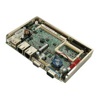
3.5" SBC with Intel Atom Processor with support for VGA and LVDS Displays, Dual PCIe GbE, CF Type II, and SATA
Brand:
IEI Technology
| Category:
Motherboard
| Size: 8 MB
Table of Contents
Table of Contents
4
User Manual
1
1 Introduction
16
Introduction
17
Model Variations
17
Figure 1-1: WAFER-945GSE
17
Table 1-1: WAFER-945GSE Model Variations
17
Connectors
18
Figure 1-2: Connectors
18
Dimensions
20
Figure 1-3: WAFER-945GSE Dimensions (MM)
20
Data Flow
21
Figure 1-4: Data Flow Diagram
21
Technical Specifications
22
Table 1-2: WAFER-945GSE Specifications
23
2 Packing List
24
Anti-Static Precautions
25
Unpacking Precautions
25
Packing List
26
Optional Items
27
Table 2-1: Packing List
27
Table 2-2: Optional Items
27
3 Connectors
28
Peripheral Interface Connectors
29
Figure 3-1: Connectors and Jumpers
29
WAFER-945GSE Layout
29
External Interface Panel Connectors
30
Table 3-1: Peripheral Interface Connectors
30
Table 3-2: Rear Panel Connectors
30
Internal Peripheral Connectors
31
ATX Power Connector
31
ATX Power Supply Enable Connector
31
Figure 3-2: ATX Power Connector Location
31
Table 3-3: ATX Power Connector Pinouts
31
Audio Connector (10-Pin)
32
Figure 3-3: ATX Power Supply Enable Connector Location
32
Table 3-4: ATX Power Supply Enable Connector Pinouts
32
Backlight Inverter Connector
33
Figure 3-4: Audio Connector Pinouts (10-Pin)
33
Table 3-5: Audio Connector Pinouts (10-Pin)
33
Compactflash® Socket
34
Figure 3-5: Panel Backlight Connector Location
34
Table 3-6: Panel Backlight Connector Pinouts
34
Figure 3-6: CF Card Socket Location
35
Digital Input/Output (DIO) Connector
36
Figure 3-7: Digital I/O Connector Location
36
Table 3-7: CF Card Socket Pinouts
36
Table 3-8: Digital I/O Connector Pinouts
36
Fan Connector (+12V, 3-Pin)
37
Figure 3-8: +12V Fan Connector Location
37
Keyboard/Mouse Connector
37
Table 3-9: +12V Fan Connector Pinouts
37
Figure 3-9: Keyboard/Mouse Connector Location
38
LED Connector
38
Table 3-10: Keyboard/Mouse Connector Pinouts
38
Figure 3-10: LED Connector Location
39
LVDS LCD Connector
39
Table 3-11: LED Connector Pinouts
39
Figure 3-11: LVDS LCD Connector Pinout Locations
40
Table 3-12: LVDS LCD Port Connector Pinouts
40
Figure 3-12: Pcie Mini Card Slot Location
41
Pcie Mini Card Slot
41
Power Button Connector
42
Table 3-13: Pcie Mini Card Slot Pinouts
42
Figure 3-13: Power Button Connector Location
43
Figure 3-14: Reset Button Connector Location
43
Reset Button Connector
43
Table 3-14: Power Button Connector Pinouts
43
Figure 3-15: SATA Drive Connector Locations
44
SATA Drive Connectors
44
Table 3-15: Reset Button Connector Pinouts
44
Table 3-16: SATA Drive Connector Pinouts
44
Figure 3-16: COM3 to COM6 Connector Pinout Locations
45
Serial Port Connectors, RS-232
45
Serial Port Connector, RS-232/422/485
46
Table 3-17: COM3 to COM6 Connector Pinouts
46
Figure 3-17: RS-232/422/485 Serial Port Connector Location
47
SPI Flash Connector
47
Table 3-18: RS-232/422/485 Serial Port Connector Pinouts
47
Figure 3-18: SPI Flash Connector
48
Table 3-19: SPI Flash Connector
48
USB Connectors (Internal)
48
External Peripheral Interface Connector Panel
49
Figure 3-19: USB Connector Pinout Locations
49
Figure 3-20: External Peripheral Interface Connector
49
Table 3-20: USB Port Connector Pinouts
49
Ethernet Connectors
50
Figure 3-21: RJ-45 Ethernet Connector
50
Table 3-21: LAN Pinouts
50
Table 3-22: RJ-45 Ethernet Connector Leds
50
Figure 3-22: COM1 Pinout Locations
51
Serial Port Connectors (COM1)
51
Table 3-23: RS-232 Serial Port (COM 1) Pinouts
51
USB Connectors
51
Figure 3-23: VGA Connector
52
Table 3-24: USB Port Pinouts
52
Table 3-25: VGA Connector Pinouts
52
VGA Connector
52
4 Installation
53
Anti-Static Precautions
54
Installation Considerations
54
So-DIMM and Cf Card Installation
56
Figure 4-1: SO-DIMM Installation
56
SO-DIMM Installation
56
CF Card Installation
57
Figure 4-2: CF Card Installation
57
Jumper Settings
58
AT Power Select Jumper
58
Table 4-1: Jumpers
58
CF Card Setup
59
Figure 4-3: at Power Select Jumper Location
59
Table 4-2: at Power Select Jumper Settings
59
Clear CMOS Jumper
60
Figure 4-4: CF Card Setup Jumper Location
60
Table 4-3: CF Card Setup Jumper Settings
60
COM 2 Function Select Jumper
61
Figure 4-5: Clear BIOS Jumper Location
61
Table 4-4: Clear BIOS Jumper Settings
61
Table 4-5: COM 2 Function Select Jumper Settings
61
Figure 4-6: COM 2 Function Select Jumper Location
62
LVDS1 Panel Resolution Jumper
62
Table 4-6: LVDS Panel Resolution Jumper Settings
62
Figure 4-7: LVDS Panel Resolution Jumper Pinout Locations
63
LVDS Voltage Selection
63
Table 4-7: LVDS Voltage Selection Jumper Settings
63
Chassis Installation
64
Airflow
64
Figure 4-8: LVDS Voltage Selection Jumper Pinout Locations
64
Motherboard Installation
65
Internal Peripheral Device Connections
65
SATA Drive Connection
65
Figure 4-9: SATA Drive Cable Connection
66
Figure 4-10: SATA Power Cable Connection
67
Serial Port Connector Cable (Four Ports) Cable Connection
67
Dual RS-232 Cable Connection (W/O Bracket) (Optional)
68
Figure 4-11: Four Serial Port Connector Cable Connection
68
4-COM Port Adapter Board Connection (Optional)
69
Figure 4-12: Dual RS-232 Cable Installation
69
Figure 4-13: 4-COM Port Adapter Board
70
Figure 4-14: Serial Device Connector
71
Keyboard/Mouse Y-Cable Connector
71
Audio Kit Installation
72
Figure 4-15: Keyboard/Mouse Y-Cable Connection
72
Figure 4-16: Audio Kit Cable Connection
73
USB Cable (Dual Port Without Bracket) (Optional)
73
External Peripheral Interface Connection
74
Figure 4-17: Dual USB Cable Connection
74
Figure 4-18: LAN Connection
75
LAN Connection
75
Serial Device Connection
75
Figure 4-19: Serial Device Connector
76
USB Connection (Dual Connector)
76
Figure 4-20: USB Connector
77
VGA Monitor Connection
77
Heat Sink Enclosure
78
Figure 4-21: VGA Connector
78
Figure 4-22: Heat Sink Retention Screws
79
5 Bios
80
Introduction
81
Starting Setup
81
Using Setup
81
BIOS Menu Bar
82
Getting Help
82
Table 5-1: BIOS Navigation Keys
82
Unable to Reboot after Configuration Changes
82
Main
83
BIOS Menu 1: Main
83
System Overview
83
Advanced
84
BIOS Menu 2: Advanced
84
System Date [XX/XX/XX]
84
System Time [XX:XX:XX]
84
CPU Configuration
85
IDE Configuration
85
BIOS Menu 3: CPU Configuration
85
BIOS Menu 4: IDE Configuration
86
ATA/IDE Configuration [Compatible]
86
Legacy IDE Channels [SATA Pri, PATA Sec]
86
IDE Master, IDE Slave
87
BIOS Menu 5: IDE Master and IDE Slave Configuration
87
IDE Master and IDE Slave
87
Auto-Detected Drive Parameters
88
Type [Auto]
88
Block (Multi Sector Transfer) [Auto]
89
Lba/Large Mode [Auto]
89
DMA Mode [Auto]
90
PIO Mode [Auto]
90
32Bit Data Transfer [Enabled]
91
Auto]
91
Super IO Configuration
92
BIOS Menu 6: Super IO Configuration
92
Serial Port1 Address [3F8/IRQ4]
92
Serial Port2 Address [2F8/IRQ3]
93
Serial Port3 Address [3E8]
93
Serial Port3 IRQ [11]
93
Serial Port4 Address [2E8]
93
Serial Port4 IRQ [11]
94
Serial Port5 Address [2F0]
94
Serial Port5 IRQ [11]
94
Serial Port6 Address [2E0]
94
Hardware Health Configuration
95
BIOS Menu 7: Hardware Health Configuration
95
Serial Port6 IRQ [11]
95
CPU FAN Mode Setting [Full on Mode]
96
CPU Temperature Limit of off [000]
96
CPU Fan Start PWM [070]
97
CPU Temperature Limit of on [020]
97
Slope PWM [0.5 PWM]
97
Power Configuration
99
BIOS Menu 8: Power Configuration
99
Select AT/ATX Power [By HARDWARE]
99
ACPI Configuration
100
APM Configuration
100
BIOS Menu 9: ACPI Configuration
100
Suspend Mode [S1 (POS)]
100
BIOS Menu 10: Advanced Power Management Configuration
101
Power Button Mode [On/Off]
101
Restore on AC Power Loss [Last State]
101
Resume on Keyboard/Mouse [Disabled]
101
Resume on PCI-Express WAKE# [Enabled]
102
Resume on Ring [Disabled]
102
Resume on RTC Alarm [Disabled]
102
Remote Access Configuration
103
BIOS Menu 11: Remote Access Configuration
103
Remote Access [Disabled]
103
Base Address, IRQ [3F8H,4]
104
Serial Port Mode [115200 8,N,1]
104
Serial Port Number [COM1]
104
Redirection after BIOS POST [Always]
105
Terminal Type [ANSI]
105
USB Configuration
105
BIOS Menu 12: USB Configuration
106
Legacy USB Support [Enabled]
106
USB 2.0 Controller [Enabled]
106
USB Function [Enabled]
106
Pci/Pnp
107
USB 2.0 Controller Mode [Hispeed]
107
BIOS Menu 13: Pci/Pnp Configuration
108
IRQ# [Available]
108
DMA Channel# [Available]
109
Reserved Memory Size [Disabled]
109
Boot
110
Boot Settings Configuration
110
BIOS Menu 14: Boot
110
BIOS Menu 15: Boot Settings Configuration
110
Addon ROM Display Mode [Force BIOS]
111
Bootup Num-Lock [On]
111
Quick Boot [Enabled]
111
Quiet Boot [Enabled]
111
Boot Device Priority
112
Boot from LAN Support [Disabled]
112
Spread Spectrum Function [Disabled]
112
Security
113
BIOS Menu 16: Boot Device Priority Settings
113
BIOS Menu 17: Security
113
Change Supervisor Password
113
Chipset
114
BIOS Menu 18: Chipset
114
Change User Password
114
North Bridge Chipset Configuration
115
BIOS Menu 19: North Bridge Chipset Configuration
115
Internal Graphics Mode Select [Enabled, 8MB]
115
Memory Hole [Disabled]
115
Boot Display Device [Auto]
116
DVMT Mode Select [DVMT Mode]
116
DVMT/FIXED Memory [Maximum DVMT]
116
South Bridge Chipset Configuration
117
BIOS Menu 20: South Bridge Chipset Configuration
117
Audio Controller [Enabled]
117
LVDS1 Panel Type [By H/W]
117
Exit
118
BIOS Menu 21: Exit
118
Discard Changes
118
Discard Changes and Exit
118
Save Changes and Exit
118
6 Software Drivers
120
Available Software Drivers
121
Starting the Driver Program
121
Figure 6-1: Start up Screen
122
Figure 6-2: Select Operating System
122
Chipset Driver Installation
123
Figure 6-3: Drivers
123
Figure 6-4: Chipset Driver Screen
124
Figure 6-5: Chipset Driver Welcome Screen
124
Figure 6-6: Chipset Driver License Agreement
125
Figure 6-7: Chipset Driver Read Me File
126
Figure 6-8: Chipset Driver Setup Operations
126
Vga Driver Installation
127
Figure 6-9: Chipset Driver Installation Finish Screen
127
Figure 6-10: VGA Driver Read Me File
128
Figure 6-11: VGA Driver Setup Files Extracted
128
Figure 6-12: VGA Driver Welcome Screen
129
Figure 6-13: VGA Driver License Agreement
130
Figure 6-14: VGA Driver Read Me File
130
Figure 6-15: VGA Driver Setup Operations
131
Lan Driver Installation
132
Figure 6-16: VGA Driver Installation Finish Screen
132
Figure 6-17: LAN Driver Welcome Screen
133
Figure 6-18: LAN Driver Welcome Screen
133
Figure 6-19: LAN Driver Installation
134
Figure 6-20: LAN Driver Installation Complete
134
Audio Driver Installation
135
Figure 6-21: Audio Driver Installation File Extraction
135
Figure 6-22: Audio Driver Installation Welcome Screen
135
Figure 6-23: Audio Driver Installation
136
Figure 6-24: Audio Driver Installation Complete
136
ABIOS Options
137
Appendix A
138
B One Key Recovery
141
One Key Recovery Introduction
142
Figure B-1: IEI One Key Recovery Tool Menu
142
B.1 O Ne K Ey R Ecovery I Ntroduction
142
System Requirement
143
Supported Operating System
144
Setup Procedure for Windows
145
Hardware and BIOS Setup
145
Create Partitions
146
Figure B-2: Launching the Recovery Tool
146
Figure B-3: Recovery Tool Setup Menu
147
Figure B-4: Command Mode
147
Figure B-5: Partition Creation Commands
148
Install Operating System, Drivers and Applications
149
Build-Up Recovery Partition
150
Figure B-6: Launching the Recovery Tool
150
Figure B-7: System Configuration for Windows
150
Figure B-8: Build-Up Recovery Partition
151
Figure B-9: Press any Key to Continue
151
Create Factory Default Image
152
Figure B-10: Press F3 to Boot into Recovery Mode
152
Figure B-11: Recovery Tool Menu
152
Figure B-12: about Symantec Ghost Window
153
Figure B-13: Symantec Ghost Path
153
Figure B-14: Select a Local Source Drive
154
Figure B-15: Select a Source Partition from Basic Drive
154
Figure B-16: File Name to Copy Image to
155
Figure B-17: Compress Image
155
Figure B-18: Image Creation Confirmation
156
Figure B-19: Image Creation Process
156
Figure B-20: Image Creation Complete
156
Setup Procedure for Linux
157
Figure B-21: Press any Key to Continue
157
Figure B-22: Partitions for Linux
158
Figure B-23: System Configuration for Linux
159
Figure B-24: Access Menu.lst in Linux (Text Mode)
159
Recovery Tool Functions
160
Figure B-25: Recovery Tool Menu
160
B.4 R Ecovery T Ool F Unctions
160
Figure B-26: Recovery Tool Main Menu
161
Factory Restore
162
Figure B-27: Restore Factory Default
162
Figure B-28: Recovery Complete Window
162
Backup System
163
Figure B-29: Backup System
163
Figure B-30: System Backup Complete Window
163
Figure B-31: Restore Backup
164
Figure B-32: Restore System Backup Complete Window
164
Restore Your Last Backup
164
Figure B-33: Symantec Ghost Window
165
Manual
165
Other Information
166
B.5 O Ther I Nformation
166
Using AHCI Mode or Ali M5283 / VIA VT6421A Controller
166
System Memory Requirement
168
C Terminology
169
D Digital I/O Interface
173
Introduction
174
Dio Connector Pinouts
174
Assembly Language Samples
174
D.1 I Ntroduction
174
Enable the DIO Input Function
174
Enable the DIO Output Function
175
E Watchdog Timer
176
F Hazardous Materials Disclosure
179
Hazardous Materials Disclosure Table for IPB Products Certified as Rohs Compliant under 2002/95/EC Without Mercury
180
Advertisement
IEI Technology WAFER-945GSE User Manual (203 pages)
3.5” SBC with Intel Atom N270 1.6G, VGA/LVDS, Dual GbE, CF Type II,. USB, SATA, 1 GB on-board Memory and PC/104
Brand:
IEI Technology
| Category:
Single board computers
| Size: 9 MB
Table of Contents
Table of Contents
7
List of Figures
13
Introduction
21
Overview
22
WAFER-945GSE Introduction
22
Wafer-945Gse Overview
22
Front Side Bus (FSB)
22
WAFER-945GSE Overview Photo
22
Figure 1-2: WAFER-945GSE Overview [Front View]
23
WAFER-945GSE Peripheral Connectors and Jumpers
23
Technical Specifications
24
Table 1-1: Technical Specifications
26
Detailed Specifications
27
Dimensions
28
Board Dimensions
28
External Interface Panel Dimensions
29
Data Flow
29
Figure 2-1: WAFER-945GSE Dimensions (MM)
29
Figure 2-2: External Interface Panel Dimensions (MM)
29
Embedded Wafer-945Gse Processor
30
Figure 2-3: Data Flow Block Diagram
30
Overview
30
Features
31
Figure 2-4: Embedded Processor
31
Figure 2-5: Front Side Bus
32
Intel 945Gse Northbridge Chipset
33
Intel® 945GSE DDR2 Controller
33
Intel® 945GSE Overview
33
Figure 2-6: DDR2 SO-DIMM Socket
34
Intel® 945GSE Graphics
34
Analog CRT Graphics Mode
35
Figure 2-8: LVDS Connector
36
LVDS Interface
36
Intel ® Ich7-M Southbridge Chipset
37
Figure 2-9: Direct Media Interface
37
Intel ® ICH7-M Overview
37
Figure 2-10: Audio Codec and Connectors
38
Intel ® ICH7-M Audio Codec '97 Controller
38
Intel ® ICH7-M Low Pin Count (LPC) Interface
40
Intel ® ICH7-M Pcie Bus
40
Pcie Gbe Ethernet
40
Figure 2-11: Realtek RTL8111C Pcie Gbe Controllers
41
Pcie Mini Expansion Slot
42
Figure 2-12: Pcie Mini Slot
43
Intel ® ICH7-M Real Time Clock
43
Figure 2-13: SATA Connectors
44
Figure 2-14: Onboard USB Implementation
45
LPC Bu Component
45
Ite IT8718F Super I/O Chipset 2
46
Super I/O LPC Interface 2
47
Super I/O Fan Speed Controller 2
48
Operating Temperature and Temperature Control 2
49
Table 2-1: Power Consumption
50
Unpacking 3
51
A Nti - Static P Recautions 3
52
U Npacking C Hecklist 3
53
Optional Items 3
54
Connectors 3
55
Figure 4-1: Connector and Jumper Locations [Front Side]
56
P Eripheral I Nterface C Onnectors 3
56
External Interface Panel Connectors 3
57
Table 4-1: Peripheral Interface Connectors
57
Figure 4-2: ATX Power Connector Location
58
I Nternal P Eripheral C Onnectors 3
58
Table 4-2: Rear Panel Connectors
58
Figure 4-3: ATX Power Supply Enable Connector Location
59
Table 4-3: ATX Power Connector Pinouts
59
Figure 4-4: Audio Connector Pinouts (10-Pin)
60
Table 4-4: ATX Power Supply Enable Connector Pinouts
60
Table 4-5: Audio Connector Pinouts (10-Pin)
60
Backlight Inverter Connector 4
61
Figure 4-5: Panel Backlight Connector Pinout Locations
61
Table 4-6: Panel Backlight Connector Pinouts
61
F Igure 1-1: WAFER-945GSE
62
Figure 4-6: CF Card Socket Location
62
Compactflash® Socket 4
62
Table 4-7: CF Card Socket Pinouts
63
Digital Input/Output (DIO) Connector 4
63
Figure 4-7: DIO Connector Connector Locations
64
Table 4-8: DIO Connector Connector Pinouts
64
Fan Connector (+12V, 3-Pin) 4
64
Figure 4-8: +12V Fan Connector Location
65
Table 4-9: +12V Fan Connector Pinouts
65
Keyboard/Mouse Connector 4
65
Figure 4-9: Keyboard/Mouse Connector Location
66
Table 4-10: Keyboard/Mouse Connector Pinouts
66
LED Connector 4
66
Figure 4-10: LED Connector Locations
67
Table 4-11: LED Connector Pinouts
67
LVDS LCD Connector 4
67
Figure 4-11: LVDS LCD Connector Pinout Locations
68
Table 4-12: LVDS LCD Port Connector Pinouts
68
Figure 4-12: Pcie Mini Card Slot Location
69
Table 4-13: Pcie Mini Card Slot Pinouts
70
Figure 4-13: Power Button Connector Location
71
Table 4-14: Power Button Connector Pinouts
71
Figure 4-14: Reset Button Connector Locations
72
Table 4-15: Reset Button Connector Pinouts
72
SATA Drive Connectors 5
72
Figure 4-15: SATA Drive Connector Locations
73
Table 4-16: SATA Drive Connector Pinouts
73
Serial Port Connector (COM3, COM4, COM5 and COM6) 5
73
Figure 4-16: COM3 to COM6 Connector Pinout Locations
74
Table 4-17: COM3 to COM6 Connector Pinouts
75
Serial Port Connector (COM 2)(RS-232, RS-422 or RS-485) 5
75
Figure 4-17: RS-232/422/485 Serial Port Connector Location
76
Table 4-18: RS-232/RS-485 Serial Port Connector Pinouts
76
USB Connectors (Internal) 5
76
Figure 4-18: USB Connector Pinout Locations
77
Table 4-19: USB Port Connector Pinouts
77
E Xternal P Eripheral I Nterface C Onnector P Anel 5
77
Figure 4-19: WAFER-945GSE External Peripheral Interface Connector
78
Table 4-20: LAN Pinouts
78
LAN Connectors 5
78
Figure 4-20: RJ-45 Ethernet Connector
79
Table 4-21: RJ-45 Ethernet Connector Leds
79
Serial Port Connector (COM1) 5
79
Figure 4-21: COM1 Pinout Locations
80
Table 4-22: RS-232 Serial Port (COM 1) Pinouts
80
USB Connectors 6
80
F Igure 2-7: VGA Connector
81
F Igure 4-22: VGA Connector
81
Table 4-23: USB Port Pinouts
81
Table 4-24: VGA Connector Pinouts
82
Installation 6
83
A Nti - Static P Recautions 6
84
I Nstallation C Onsiderations 6
85
Installation Checklist 6
86
Figure 5-1: SO-DIMM Installation
87
Unpacking
87
CF Card Installation 6
88
Figure 5-2: CF Card Installation
89
Figure 5-3: Jumper Locations
89
Jumper Settings
89
Table 5-1: Jumpers
90
AT Power Select Jumper Settings 7
90
Figure 5-4: at Power Select Jumper Location
91
Table 5-2: at Power Select Jumper Settings
91
Table 5-3: CF Card Setup Jumper Settings
91
Figure 5-5: CF Card Setup Jumper Location
92
Clear CMOS Jumper 7
92
Figure 5-6: Clear CMOS Jumper
93
Table 5-4: Clear CMOS Jumper Settings
93
COM 2 Function Select Jumper 7
93
Figure 5-7: COM 2 Function Select Jumper Location
94
Table 5-5: COM 2 Function Select Jumper Settings
94
LVDS1 Panel Resolution Jumper 7
94
Figure 5-8:LVDS Panel Resolution Jumper Pinout Locations
95
Table 5-6: LVDS Panel Resolution Jumper Settings
95
Table 5-7: LVDS Voltage Selection Jumper Settings
96
Figure 5-9: LVDS Voltage Selection Jumper Pinout Locations
97
C Hassis I Nstallation 7
97
Table 5-8: IEI Provided Cables
98
Motherboard Installation 7
98
Figure 5-10: SATA Drive Cable Connection
99
Figure 5-11: SATA Power Drive Connection
100
Serial Port Connector Cable (Four Ports) Cable Connection 8
100
Figure 5-12: Four Serial Port Connector Cable Connection
101
Dual RS-232 Cable Connection (W/O Bracket) (Optional) 8
101
Figure 5-13: Dual RS-232 Cable Installation
102
COM Port Adapter Board Connection (Optional) 8
102
Figure 5-14: 4-COM Port Adapter Board
103
Figure 5-15: Serial Device Connector
104
Keyboard/Mouse Y-Cable Connector 8
104
Figure 5-16: Keyboard/Mouse Y-Cable Connection
105
Audio Kit Installation 8
105
Figure 5-17: Audio Kit Cable Connection
106
USB Cable (Dual Port Without Bracket) (Optional) 8
106
Figure 5-18: Dual USB Cable Connection
107
E Xternal P Eripheral I Nterface C Onnection 8
107
Figure 5-19: LAN Connection
108
LAN Connection (Single Connector) 8
108
Figure 5-20: Serial Device Connector
109
Serial Device Connection 8
109
Figure 5-21: USB Connector
110
USB Connection (Dual Connector) 9
110
VGA Monitor Connection 9
111
Figure 5-23: Heat Sink Retention Screws
113
Bios Screens 9
114
I Ntroduction 9
115
Table 6-1: BIOS Navigation Keys
116
Getting Help 9
116
Main
117
Advanced
118
CPU Configuration 9
119
IDE Configuration 1
120
IDE Master, IDE Slave 1
122
Super IO Configuration 1
128
Hardware Health Configuration 1
131
Power Configuration 1
135
ACPI Configuration 1
136
APM Configuration 1
137
Remote Configuration 1
140
USB Configuration 1
144
Pci/Pnp
146
Boot
149
Boot Device Priority 1
152
Chipset
154
North Bridge Chipset Configuration 1
155
Southbridge Configuration 1
157
Exit
158
Software Drivers 1
161
Figure 7-1: Start up Screen
163
Figure 7-2: Select Operating System
163
C Hipset D River I Nstallation 1
164
Figure 7-3: Drivers
164
Figure 7-4: Chipset Driver Screen
165
Figure 7-5: Chipset Driver Welcome Screen
165
Figure 7-6: Chipset Driver License Agreement
166
Figure 7-7: Chipset Driver Read Me File
167
Figure 7-8: Chipset Driver Setup Operations
168
Figure 7-9: Chipset Driver Installation Finish Screen
169
Vga D River I Nstallation 1
169
Figure 7-10: VGA Driver Read Me File
170
Figure 7-11: VGA Driver Setup Files Extracted
170
Figure 7-12: VGA Driver Welcome Screen
171
Figure 7-13: VGA Driver License Agreement
172
Figure 7-14: VGA Driver Read Me File
172
Figure 7-15: VGA Driver Setup Operations
173
Figure 7-16: VGA Driver Installation Finish Screen
173
Figure 7-17: LAN Driver Welcome Screen
174
Lan D River I Nstallation 1
174
Figure 7-18: LAN Driver Welcome Screen
175
Figure 7-19: LAN Driver Installation
175
Audio Driver Installation
176
Figure 7-20: LAN Driver Installation Complete
176
Figure 7-21: Audio Driver Options
177
Figure 7-22: AC'97 Driver Installation File Extraction
177
Figure 7-23: AC'97 Driver Installation Welcome Screen
178
Figure 7-24: AC'97 Driver Installation Verification
178
Figure 7-25: AC'97 Driver Installation
179
Figure 7-26: AC'97 Driver Installation Complete
179
A Bios Menu Options 1
180
B Terminology 1
184
C Dio Interface 1
189
F Igure 2-15: Super I
190
C .1 Dio I Nterface I Ntroduction 1
190
C .3.1 Enable the DIO Input Function 1
191
D Watchdog Timer 1
192
E Address Mapping 1
195
E.1 I/O Addres Map
196
E.2 IRQ Addres Map
198
Advertisement
Related Products
IEI Technology WAFER-945GSELVDS2
IEI Technology WAFER-945GSE2
IEI Technology WAFER-9102
IEI Technology WAFER-945GSELVDS2-N270-R10
IEI Technology Wafer-CX700m
IEI Technology WAFER-PV-D4251
IEI Technology WAFER-PV-D5253
IEI Technology WAFER-4823
IEI Technology WAFER-4821
IEI Technology WAFER-LX-WINXPE
IEI Technology Categories
Motherboard
Touch Panel
Computer Hardware
Single board computers
Desktop
More IEI Technology Manuals
Login
Sign In
OR
Sign in with Facebook
Sign in with Google
Upload manual
Upload from disk
Upload from URL