Sign In
Upload
Download
Table of Contents
Contents
Add to my manuals
Delete from my manuals
Share
URL of this page:
HTML Link:
Bookmark this page
Add
Manual will be automatically added to "My Manuals"
Print this page
×
Bookmark added
×
Added to my manuals
Manuals
Brands
Kirisun Manuals
Radio
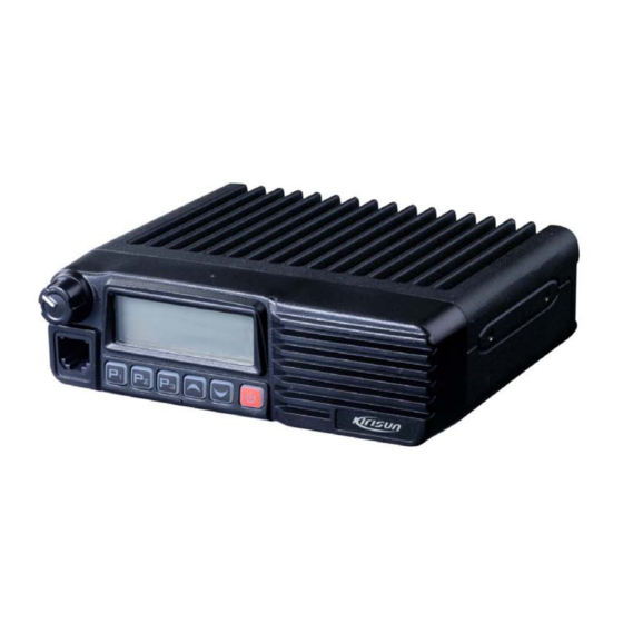
PT8100 -01
Service manual
Kirisun PT8100 -01 Service Manual
Pt8100 series. vhf/uhf mobile radio
Hide thumbs
1
Table Of Contents
2
3
4
5
6
7
8
9
10
11
12
13
14
15
16
17
18
19
20
21
22
23
24
25
26
27
28
29
30
31
32
33
34
35
page
of
35
Go
/
35
Contents
Table of Contents
Troubleshooting
Bookmarks
Table of Contents
Table of Contents
Chapter 1 Overview
Chapter 2 Unpacking and Checking
Chapter 3 External View and Functional Keys
Chapter 4 Circuit Description
Chapter 5 Mode Introduction
Chapter 6 Disassembly and Assembly for Maintenance
Chapter 7 Adjustment
Chapter 8 Specifications
Chapter 9 Troubleshooting
Appendix 2 Electronic Parts List
Appendix 1 Abbreviations
Appendix 4 Accessories
Figure 1 PT8100 Block Diagram
Figure 2 PT8100 Main Board Schematic Circuit Diagram
Figure 3 PT8100 Main Board Top Layer Position Mark Diagram
Figure 4 PT8100 Main Board Top Layer Position Value Diagram
Figure 5 PT8100 Main Board Bottom Layer Position Mark Diagram
Figure 6 PT8100 Main Board Bottom Layer Position Value Diagram
Figure 7 PT8100 Key Board Schematic Circuit Diagram
Figure 8 PT8100 Key Board Top Layer Position Mark Diagram
Figure 9 PT8100 Key Board Top Layer Position Value Diagram
Figure 10 PT8100 Key Board Bottom Layer Position Mark Diagram
Figure 11 PT8100 Key Board Bottom Layer Position Value Diagram
Appendix 3 Structural Parts List
Advertisement
Quick Links
1
Chapter 3 External View and Functional Keys
2
Chapter 4 Circuit Description
3
Chapter 5 Mode Introduction
4
Chapter 7 Adjustment
5
Chapter 8 Specifications
6
Appendix 4 Accessories
7
Figure 1 Pt8100 Block Diagram
8
Figure 2 Pt8100 Main Board Schematic Circuit Diagram
Download this manual
Table of
Contents
Previous
Page
Next
Page
1
2
3
4
5
Advertisement
Table of Contents
Need help?
Do you have a question about the PT8100 -01 and is the answer not in the manual?
Ask a question
Questions and answers
Related Manuals for Kirisun PT8100 -01
Radio Kirisun PT8200 Service Manual
Vhf /uhf mobile radio (42 pages)
Radio Kirisun PT8100 Instruction Manual
Kirisun pt8100 vhf/uhf mobile radio (12 pages)
Radio Kirisun PT810001 Instruction Manual
Vhf/uhf mobile radio (15 pages)
Radio Kirisun PT810003 Instruction Manual
Vhf/uhf mobile radio (15 pages)
Radio Kirisun PT4208 Service Manual
Fm portable radio (53 pages)
Radio Kirisun PT8000 Service Manual
Professional two-way radio (32 pages)
Radio Kirisun PT8000 Service Manual
Vhf/uhf mobile radio (28 pages)
Radio Kirisun PT8100 -02 Service Manual
Pt8100 series. vhf/uhf mobile radio (35 pages)
Radio Kirisun PT6808-02 Service Manual
Pt6808 series. vhf/uhf mobile radio (62 pages)
Radio Kirisun DP990 Service Manual
(76 pages)
Radio Kirisun GP700 Service Manual
(23 pages)
Radio Kirisun TM840 Service Manual
(104 pages)
Radio Kirisun FP420 Service Manual
Fm portable radios (50 pages)
Radio Kirisun DM588-01 User Manual
Digital mobile radio (64 pages)
Radio Kirisun DM588 Service Manual
(151 pages)
Radio Kirisun DP770 Service Manual
(103 pages)
This manual is also suitable for:
Pt8100 -02
Table of Contents
Print
Rename the bookmark
Delete bookmark?
Delete from my manuals?
Login
Sign In
OR
Sign in with Facebook
Sign in with Google
Upload manual
Upload from disk
Upload from URL


Need help?
Do you have a question about the PT8100 -01 and is the answer not in the manual?
Questions and answers