Table of Contents
Advertisement
Quick Links
Download this manual
See also:
Quick Manual
Advertisement
Table of Contents

Related Manuals for Acrosser Technology ACE-B8701


Summary of Contents for Acrosser Technology ACE-B8701
-
Page 1: User Manual
Revision: 1.0 ACE-B8701 Board PCI I/O Board with discrete I/O, battery backup SRAM, Timer, Power-off intrusion Event Logger and Protect-U User Manual Manual Rev.: 1.0 Book Number: ACE-B8701-2010.08.19... - Page 2 Revision: 1.0 Revision Version Date Author Description 2010/08/19 Kenny Lee Initial release...
- Page 3 Trademarks ACE-B8701 is a registered trademarks of Acrosser; IBM PC is a registered trademark of the International Business Machines Corporation; Pentium is a registered trademark of Intel Technologies Inc; Award is a registered trademark of Award Software International Inc;...
-
Page 4: Table Of Contents
Revision: 1.0 Table of Contents 1 Introduction................5 1.1 Specifications .................. 6 1.2 Package Contents ................6 1.3 Block Diagram ................. 7 2 H/W Information ............... 8 2.1 Locations (Top Side) ............... 8 2.2 Connector and Jumper Setting ............9 2.3 Connector and Jumper Setting Table .......... -
Page 5: Introduction
This gaming controller features digital input, digital output, SRAM, timer, intrusion logger, secured real time clock and security ID. Together with the software development kit (SDK), ACE-B8701 is very easy to control devices in a gaming machine. Please refer to following specification for detail functions. -
Page 6: Specifications
Single 256KB battery back-up SRAM with battery low monitor for each battery Secondary real time clock One 8-bit readable DIP switch 6 watts Stereo amplifier 1.2 Package Contents Check if the following items are included in the package. Quick Manual ACE-B8701 board 1 x Software Utility CD... -
Page 7: Block Diagram
Revision: 1.0 1.3 Block Diagram C7 nano DDRII DIMM X 1 DDRII 512MB onboard CRT1 VX800 SATAX2 COM PORT*2 CFX1 VT1625 CRT2 USB Port X4 LPC BUS PCI BUS SPI ROM Fintek EtherNET 10/100M HD Link PORT*4 HD CODEC 6W A RJ-45 class... -
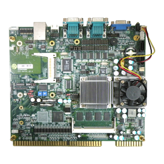
Page 8: W Information
Revision: 1.0 H/W INFORMATION This chapter describes the installation of ACE-B8701. At first, it shows the Function diagram and the layout of ACE-B8701. It then describes the unpacking information which you should read carefully, as well as the jumper/switch settings for the ACE-B8701 configuration. -
Page 9: Connector And Jumper Setting
Revision: 1.0 2.2 Connector and Jumper Setting 2.2.1 Locations (Top side) - Page 10 Revision: 1.0 2.2.2 List of Connector and Jumper Setting CCTALK1 JST connector for ccTalk JST connector for Keyboard (Signal share with 8-bit readable DIP switch. and Mouse. COM6). COM6(optional) JST connector for Case Pin header for 2 USB ports. Pin header for RS232 port. Open Intrusion logger.
-
Page 11: Connector And Jumper Setting Table
Revision: 1.0 2.3 Connector and Jumper Setting Table 1. CCTALK1 2. KM1 3. SW1 Signal Signal Mouse data DATA Keyboard data Status Signal 3.3V Mouse clock Keyboard clock 4. CN4 5. CN3 6. COM6 Signal Signal Signal Signal -DCD -DSR Signal -USB0 -USB2... - Page 12 Revision: 1.0 10. BAT3 11. VR1/VR2 12. JPB_1/JPB_2 JPB_1 JPB_2 Setting Setting SPEAKER Audio RIGHT+ connect to 72 1-3, with Pins Golden Amplifier Fingers(B5, Signal close Adjust volume level by turning VR clockwise (default) 3.3V (default) SPEAKER Audio RIGHT+ 3-5, connect to 72 without Pins Golden...
- Page 13 Revision: 1.0 19. FAN1 20. JPA_1/JPA_2/JPA_3/JPA_5 JPA_1 & JPA_3 JPA_5 JPA_2 Setting Setting Setting Signal 1-2, 4-5, 7-8, 10-11, ccTalk RS485 13-14, 16-17, 19-20, Output output output 22-23 Close 2-3, 5-6, 8-9, 11-12, RS232 output RS232 output RS232 output 14-15, 17-18, 20-21, (default) (default) (default)
-
Page 14: Bios Setting
Revision: 1.0 BIOS SETTING This chapter describes the BIOS menu displays and explains how to perform common tasks needed to get the system up and running. It also gives detailed explanation of the elements found in each of the BIOS menus. The following topics are covered: Main Setup Advanced Chipset Setup... -
Page 15: Main Setup
Revision: 1.0 3.1 Main Setup Once you enter the Award BIOS™ CMOS Setup Utility, the Main Menu will appear on the screen. Use the arrow keys to highlight the item and then use the <Pg Up> <Pg Dn> keys to select the value you want in each item. Note: Listed at the bottom of the menu are the control keys. -
Page 16: Advanced Chipset Setup
Revision: 1.0 3.2 Advanced Chipset Setup Option Choice Description This category speeds up Power On Self Test (POST) after you Quick Power On Self Enabled have powered up the computer. If it is set to Enable, BIOS will Test Disabled shorten or skip some check items during POST. -
Page 17: Pnp/Pci Setup
Revision: 1.0 3.3 PnP/PCI setup Option Choice Description Normally, you leave this field Disabled. Select Enabled to reset Extended System Configuration Data (ESCD) when you Reset Configuration Enabled exit Setup. If you have installed a new add-on and the system Data Disabled reconfiguration has caused such a serious conflict, then the... -
Page 18: Peripherals Setup
Revision: 1.0 3.4 Peripherals Setup Option Choice Description Onboard Serial Port 1 Serial Port 1: 3F8 / IRQ11 Onboard Serial Port 2 Serial Port 2: 2F8 / IRQ10 Onboar`d Serial Port 3 Serial Port 3: 2A8 / IRQ7 Select an address and the corresponding Onboard Serial Port 4 Serial Port 4: 288 / IRQ5 interrupt for each serial port. -
Page 19: Agc Setup
Revision: 1.0 3.5 AGC Setup Option Choice Description Output Port-H I/O Mode Set Input If Port H I/O Mode is “Output” , Port-H Status 00 to FF User can modify it Output Port-I I/O Mode Set Input If Port I I/O Mode is “Output” , Port-I Status 00 to FF User can modify it... -
Page 20: Boot Setup
Revision: 1.0 3.6 Boot setup Option Choice Description Hard Disk First / Second / Third CDROM The BIOS attempts to load the operating Boot Device/Other Boot USB-FDD system from the devices in the sequence Device USB-CDROM selected in these items. Disabled These fields set the Boot Priority for each Hard Disk Boot Priority... -
Page 21: Exit Setup
Revision: 1.0 3.7 Exit Setup Option Choice Description Press “Y” to store the selections made in the menus in CMOS – a special section of Pressing <Enter> on this item memory that stays on after you turn your for confirmation: system off. - Page 22 Revision: 1.0 in length, and press <Enter>. The password typed now will clear any previous password from the CMOS memory. You will be asked to confirm the password. Type the password again and press <Enter>. You may also press <Esc> to abort the selection and not enter a password.
-
Page 23: Agc Register Description
Revision: 1.0 AGC REGISTER DESCRIPTION This chapter describes the function of the Register inside an AGC chip. To program the application’s software, an user must have the know-how of these Registers. 4.1 PCI Configuration Register PCI CFG 32 bit Register Register Offset Readable... - Page 24 Revision: 1.0 Command Register (04h : 05h) Software Software Value after Bit Field Description Readable Writable Reset I/O Space. Value of 1 allows device to respond to I/O space accesses. Memory Space. Value of 1 allows device to respond to memory space accesses Master Enable.
- Page 25 Revision: 1.0 Header Type Register (0Eh) Software Software Value after Bit Field Description Readable Writable Reset Configuration Layout Type. Specifies layout of bits 10h 22 : 16 through 3Fh in configuration space. Only one encoding 0 is defined. All other encodings are reserved. Header Type.
- Page 26 Revision: 1.0 Base Address 2 Registers (18h) Software Software Value after Bit Field Description Readable Writable Reset 31 : 0 Not Supported Base Address 3 Registers (1Ch) Software Software Value after Bit Field Description Readable Writable Reset 31 : 0 Not Supported Base Address 4 Registers (20h) Software...
- Page 27 Revision: 1.0 Interrupt Pin Registers (3Dh) Software Software Value after Bit Field Description Readable Writable Reset Interrupt Pin Register indicates the interrupt pin that the device uses. The following values are decoded: 0 = No Interrupt Pin 1 = INTA# 15 : 8 2 = INTB# 3 = INTC#...
-
Page 28: Sram Memory Address Map
Revision: 1.0 4.2 SRAM Memory Address Map The following table shows the SRAM Memory Address map (max. 1024 KB) and their offset addresses, relative to the “PCI Base Address 0”. To access SRAM memory, the user must use Byte-Access command. 32 bit Data width Memory Software... -
Page 29: I/O-Interface Address Map
Revision: 1.0 4.3 I/O-Interface Address Map The following table shows the I/O Address map, including descriptions and their offset addresses relative to the “PCI Base Address1”. 32 bit Register Software Software I/O Offset Address Readable Writable Reserved Reserved Reserved Interrupt & Timer Enable Register Reserved I/O &... - Page 30 Revision: 1.0 Port E as Input; ‘1’ = Support Interrupt from Port E as Input Port F Interrupt Enable bit. ‘0’ = No support Interrupt from Port F as Input; ‘1’ = Support Interrupt from Port F as Input Port G Interrupt Enable bit. ‘0’ = No support Interrupt from Port G as Input;...
- Page 31 Revision: 1.0 Interrupt Source Register (0Ch & 0Dh) Software Software Value after Bit Field Description Readable Writable Reset Interrupt Status in Port A. 0 = No Interrupt, 1 = Interrupt active. To clear this bit, must be wrote any data to Port A as Input Interrupt Status in Port B.
- Page 32 Revision: 1.0 Port BCD Mode (10h) Software Software Value after Bit Field Description Readable Writable Reset Port A (8 bit). 0 = Input Mode, Output Mode disable Port B (8 bit). 0 = Input Mode, 1 = Output Mode Port C (8 bit). 0 = Input Mode, 1 = Output Mode Port D (8 bit).
- Page 33 Revision: 1.0 Output Mode) Bit 4 of Port C 0 / 1 Yes (only in Output Mode) Bit 5 of Port C 0 / 1 Yes (only in Output Mode) Bit 6 of Port C 0 / 1 Yes (only in Output Mode) Bit 7 of Port C 0 / 1...
- Page 34 Revision: 1.0 Bit 8 of Port E Yes (only in 0 / 1 Output Mode) Port F Data (2Ch) Software Software Value after Bit Field Description Readable Writable Reset Yes (only in Bit 1 of Port F 0 / 1 Output Mode) Bit 2 of Port F Yes (only in...
- Page 35 Revision: 1.0 Bit 7 of Port H Yes (only in 0 / 1 Output Mode) Bit 8 of Port H Yes (only in 0 / 1 Output Mode) Port IJ Mode (38h) Software Software Value after Bit Field Description Readable Writable Reset Port I (8 bit).
- Page 36 Revision: 1.0 Timer-B Register (50h & 51h) Software Software Value after Bit Field Description Readable Writable Reset 16 bits Timer-B up to 1 to 65535 mS. If this register is written, Yes, only if 0 - 15 the Timer-B will count down and if “0” state is reached, it will Timer-B is generate an interrupt.
-
Page 37: Electrical Characteristics
+5V power input 4.85 5.25 ccTalk Communication pin high threshold threshold ccTalk Communication pin low level Threshold -0.3 RS232 Maximum Working baud rate 115.2 Kbps Maximum Working baud rate 19.2 Kbps Total power consumption in ACE-B8701 T.P.C without External device... -
Page 38: Pins Golden Finger
Revision: 1.0 5.2 72 Pins Golden Finger Component Side Solder Side I/O TYPE Port/Bit Function Function Port/Bit I/O TYPE SPEAKER Audio GND RIGHT+ SPEAKER Audio GND LEFT + Button 1 Audio GND SPEAKER Button 2 RIGHT+ Button 3 Door SW2 Button 4 Door SW3 Button 5... -
Page 39: Pins Golden Finger
Revision: 1.0 5.3 20 Pins Golden Finger Component Side Solder Side I/O TYPE Port/Bit Function Function Port/Bit I/O TYPE +12V +12V +12V +12V Hopper SSR... -
Page 40: Agc Port Assignment
Revision: 1.0 5.4 AGC Port Assignment Port/Bit 72 Pins Remark Door SW1 AGA intrusion bit 0 Door SW2 AGA intrusion bit 1 Door SW3 AGA intrusion bit 2 Door SW4 AGA intrusion bit 3 Door SW5 AGA intrusion bit 4 Power on/off AGA intrusion bit 5 Chassis Switch... - Page 41 Revision: 1.0 Lamp12 Lamp13 Lamp14 Lamp15 Lamp16 Key-In Meter Bill-In Meter Coin-In Meter Pay-Out Meter Key-Out Meter Hand-Pay Meter1 Hand-Pay Meter2 Spare Meter1 Coin-En Bill-En Hopper SSR DIP Switch Bit 0 DIP Switch Bit 1 DIP Switch Bit 2 DIP Switch Bit 3 DIP Switch Bit 4 DIP Switch Bit 5 DIP Switch Bit 6...
-
Page 42: Notes
Revision: 1.0 Notes I.I (Isolated-Input) external connection application note. - Page 43 Revision: 1.0 I (TTL Input) external connection application note. O.D (Open-Drain) output external connection application note. A.O (Audio Output) is maximum 12V peak for 8 speaker. Please don not short the R- and L- together.
- Page 44 Revision: 1.0 Notice for Rechargeable battery Please charge the battery 24hrs firstly before using. Watch Dog Timer Reset Sample Code (Fintek F81216AD) #include <conio.h> #include <stdlib.h> #include <stdio.h> #include <dos.h> int main(int argc, char *argv[]) unsigned char Time; int Temp; if ( argc != 2 ) { Show_Help();...
Need help?
Do you have a question about the ACE-B8701 and is the answer not in the manual?
Questions and answers