
Subscribe to Our Youtube Channel
Related Manuals for Acrosser Technology AR-B1476


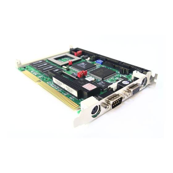
Summary of Contents for Acrosser Technology AR-B1476
- Page 1 AR-B1476 INDUSTRIAL GRADE 486DX/DX2/DX4 CPU CARD User’ s Guide Edition: 1.52 Book Number: AR-B1476-05.0525...
-
Page 3: Table Of Contents
AR-B1476 User’s Guide Table of Contents PREFACE ................................0-3 COPYRIGHT NOTICE AND DISCLAIMER..........................0-3 WELCOME TO THE AR-B1476 CPU BOARD........................0-3 BEFORE YOU USE THIS GUIDE............................0-3 RETURNING YOUR BOARD FOR SERVICE ........................0-3 TECHNICAL SUPPORT AND USER COMMENTS ....................... 0-3 ORGANIZATION .................................. - Page 4 AR-B1476 User’s Guide LOAD DEFAULT SETTING..............................6-8 6.8.1 Auto Configuration with Optimal Setting ........................6-8 6.8.2 Auto Configuration with Fail Safe Setting........................6-8 BIOS EXIT....................................6-9 6.9.1 Save Settings and Exit ..............................6-9 6.9.2 Exit Without Saving ................................ 6-9 6.10 BIOS UPDATE ...................................
-
Page 5: Preface
0.1 COPYRIGHT NOTICE AND DISCLAIMER June 1998 This document is copyrighted, 1998, by Acrosser Technology Co., Ltd. All rights are reserved. No part of this manual may be reproduced, copied, transcribed, stored in a retrieval system, or translated into any language or computer language in any form or by any means, such as electronic, mechanical, magnetic, optical, chemical, manual or other means without the prior written permission of original manufacturer. -
Page 6: Organization
AR-B1476 User’s Guide 0.6 ORGANIZATION This information for users covers the following topics (see the Table of Contents for a detailed listing): Chapter 1, “Overview”, provides an overview of the system features and packing list. Chapter 2, “System Controller” describes the major structure. -
Page 7: Overview
A super I/O chip (SMC37C669) is embedded in the AR-B1476 card. It combines functions of a floppy disk drive adapter, a hard disk drive (IDE) adapter, two serial (with 16C550 UART) adapters and 1 parallel adapter. The I/O port configurations can be done by set the BIOS setup program. -
Page 8: Packing List
AR-B1476 User’s Guide 1.2 PACKING LIST The accessories are included with the system. Before you begin installing your AR-B1476 board, take a moment to make sure that the following items have been included inside the AR-B1476 package. This user’s guide... -
Page 9: System Controller
Parallel Port 2.1 DMA CONTROLLER The equivalent of two 8237A DMA controllers are implemented in the AR-B1476 board. Each controller is a four- channel DMA device that will generate the memory addresses and control signals necessary to transfer information directly between a peripheral device and memory. This allows high speeding information transfer with less CPU intervention. -
Page 10: Interrupt Controller
AR-B1476 User’s Guide 2.3 INTERRUPT CONTROLLER The equivalent of two 8259 Programmable Interrupt Controllers (PIC) are included on the AR-B1476 board. They accept requests from peripherals, resolve priorities on pending interrupts in service, issue interrupt requests to the CPU, and provide vectors which are used as acceptance indices by the CPU to determine which interrupt service routine to execute. -
Page 11: I/O Port Address Map
AR-B1476 User’s Guide 2.3.1 I/O Port Address Map Hex Range Device 000-01F DMA controller 1 020-021 Interrupt controller 1 022-023 ALI M1489/M1487 040-04F Timer 1 050-05F Timer 2 060-06F 8042 keyboard/controller 070-071 Real-time clock (RTC), non-maskable interrupt (NMI) 080-09F DMA page registers... - Page 12 AR-B1476 User’s Guide I/O Pin Signal Name Input/Output I/O Pin Signal Name Input/Output SA14 Input/Output -DACK1 Output SA13 Input/Output DRQ1 Input SA12 Input/Output -REFRESH Input/Output SA11 Input/Output BUSCLK Output SA10 Input/Output IRQ7 Input Input/Output IRQ6 Input Input/Output IRQ5 Input Input/Output...
-
Page 13: Real-Time Clock And Non-Volatile Ram
2.4 REAL-TIME CLOCK AND NON-VOLATILE RAM The AR-B1476 contains a real-time clock compartment that maintains the date and time in addition to storing configuration information about the computer system. It contains 14 bytes of clock and control registers and 114 bytes of general purpose RAM. -
Page 14: Serial Port
AR-B1476 User’s Guide 2.6 SERIAL PORT The ACEs (Asynchronous Communication Elements ACE1 to ACE4) are used to convert parallel data to a serial format on the transmit side and convert serial data to parallel on the receiver side. The serial format, in order of transmission and reception, is a start bit, followed by five to eight data bits, a parity bit (if programmed) and one, one and half (five-bit format only) or two stop bits. - Page 15 AR-B1476 User’s Guide (5) Line Control Register (LCR) Bit 0: Word Length Select Bit 0 (WLS0) Bit 1: Word Length Select Bit 1 (WLS1) WLS1 WLS0 Word Length 5 Bits 6 Bits 7 Bits 8 Bits Bit 2: Number of Stop Bit (STB)
-
Page 16: Parallel Port
AR-B1476 User’s Guide (9) Divisor Latch (LS, MS) Bit 0: Bit 0 Bit 8 Bit 1: Bit 1 Bit 9 Bit 2: Bit 2 Bit 10 Bit 3: Bit 3 Bit 11 Bit 4: Bit 4 Bit 12 Bit 5:... - Page 17 AR-B1476 User’s Guide (4) Printer Status Buffer The system microprocessor can read the printer status by reading the address of the Printer Status Buffer. The bit definitions are described as follows: -ERROR SLCT -ACK -BUSY Figure 2-2 Printer Status Buffer NOTE: X presents not used.
- Page 18 AR-B1476 User’s Guide (5) Printer Control Latch & Printer Control Swapper The system microprocessor can read the contents of the printer control latch by reading the address of printer control swapper. Bit definitions are as follows: STROBE AUTO FD XT...
-
Page 19: Setting Up The System
Overview System Setting 3.1 OVERVIEW The AR-B1476 is a half size industrial grade CPU card that has been designed to withstand continuous operation in harsh environments. This section provides hardware’s jumpers setting, the connectors’ locations, and the pin assignment. Figure 3-1 External System Location... -
Page 20: System Setting
Press the jumper evenly onto the pins. Be careful not to bend the pins. We will show the locations of the AR-B1476 jumper pins, and the factory-default setting. CAUTION: Do not touch any electronic component unless you are safely grounded. Wear a grounded wrist strap or touch an exposed metal part of the system unit chassis. -
Page 21: Fdd Port Connector (Cn2)
To use the parallel port, an adapter cable has to be connected to the CN4 (26-pin header type) connector. This adapter cable is mounted on a bracket and is included in your AR-B1476 package. The connector for the parallel port is a 25 pin D-type female connector. -
Page 22: Pc/104 Connector
AR-B1476 User’s Guide 3.2.4 PC/104 Connector (1) 64 Pin PC/104 Connector Bus A & B (CN7) 64-Pin PC/104 Connector Figure 3-5 CN7: 64 Pin PC/104 Connector Bus A & B -IOCHCK --- --- GND SD7 --- --- RSTDRV SD6 ---... - Page 23 AR-B1476 User’s Guide (3) I/O Channel Signal Description Name Description BUSCLK [Output] The BUSCLK signal of the I/O channel is asynchronous to the CPU clock. RSTDRV [Output] This signal goes high during power-up, low line-voltage or hardware reset SA0 - SA19 The System Address lines run from bit 0 to 19.
-
Page 24: Led Header
AR-B1476 User’s Guide Name Description -MASTER [Input] The MASTER is the signal from the I/O processor which gains control as the master and should be held low for a maximum of 15 microseconds or system memory may be lost due to the lack of refresh... -
Page 25: Serial Port
AR-B1476 User’s Guide 3.2.6 Serial Port (1) RS-232/RS-485 Select (SW1, JP4 & JP9) JP4 selects COM B port, and adjusts the CN5 connector is RS-485 or RS-232C. JP9 selects COM A port for using DB2 for RS-232C or connects External RS-485. SW1 adjusts the onboard RS-485. - Page 26 (4) RS-232 Connector (CN5 & DB2) There are two serial ports with EIA RS-232C interface on the AR-B1476. COM A uses one onboard D-type 9 pin male connector (DB2) and COM B uses one 10 pin header (CN5) which are located at the right side of the card.
-
Page 27: Keyboard Connector (Cn9 & J9)
CN9 is a Mini-DIN 6-pin connector. This keyboard connector is a PS/2 type keyboard connector. This connector is also for a standard IBM-compatible keyboard with the keyboard adapter cable. J9 provides another way of connecting a keyboard to the AR-B1476. 1 DATA... -
Page 28: Reset Header (J8)
To use the PS/2 interface, an adapter cable has to be connected to the CN6 and J7 (6-pin header type) connector. This adapter cable is mounted on a bracket and is included in your AR-B1476 package. The connector for the PS/2 mouse is a Mini-DIN 6-pin connector. -
Page 29: Cpu Setting
AR-B1476 User’s Guide 3.2.12 CPU Setting The AR-B1476 accepts many types of microprocessors such as Intel/AMD/Cyrix 486DX/DX2/DX4. All of these CPUs include an integer processing unit, floating-point processing unit, memory-management unit, and cache. They can give a two to ten-fold performance improvement in speed over the 386 processor, which is depending on the clock speeds used and specific application. -
Page 30: Memory Setting
Memory Modules) which is designed to accommodate 256KX36 bit to 16MX36-bit SIMMs. This provides the user with up to 64MB of main memory. The 32-bit SIMM (without parity bit) also can be used on AR-B1476 board. There are listing on-board memory configurations available. Please refer to the following table for details:... -
Page 31: Diskonchip Installation (Sw1)
AR-B1476 User’s Guide 3.2.14 DiskOnChip Installation (SW1) The DiskOnChip is a new generation of high performance single-chip Flash Disk. It provides a Flash Disk in a standard 32-pin DIP package. This unique data storage solution offers a better, faster, and more cost-effective Flash Disk for Single Board embedded systems. -
Page 33: Crt/Lcd Flat Panel Display
Use the Flash memory Writer utility to download the new BIOS file into the ROM chip to configure the BIOS default settings for different types of LCD panels. Next, set your system properly and configure the AR-B1476 VGA module for the right type of LCD panel you are using. -
Page 34: Inverter Board Description
The inverter board supplies high voltage signals to drive the LCD panel by converting the 12 volt signal from the AR-B1476 into a high voltage AC signal for LCD panel. It can be installed freely on the space provided over the VR board. - Page 35 AR-B1476 User’s Guide (4) LCD Panel Display Connector (CN3) Attach a display panel connector to this 44-pin connector with pin assignments as shown below: Figure 4-7 CN3: LCD Display Connector Signal Signal SHFCLK P0(B0) P1(B1) P2(B2) P3(B3) P4(B4) P5(B5) P6(B6)
-
Page 37: Installation
Watchdog Timer 5.1 OVERVIEW This chapter provides information for you to set up a working system based on the AR-B1476 CPU board. Please read the details of the CPU board’s hardware descriptions before installation carefully, especially jumpers’ setting, switch settings and cable connections. -
Page 38: Vga Driver
AR-B1476 User’s Guide 5.2.1 VGA Driver (1) WIN 3.1 Driver For the WIN31 operating system, user must in the DOS mode decompress the compress file. And then as to the steps: Make the new created directory to put the VGA drivers. - Page 39 AR-B1476 User’s Guide (2) WIN 95 Driver For the WIN95 operating system, user must in the DOS mode decompress the compress file. And then as to the steps: Make the new created directory to put the VGA drivers. Step 1: C:\>MD VGAW95...
-
Page 40: Bios Flash Utility
SYSTEM icon <SCREEN> item of the <SYSTEM SETUP>. 5.2.2 BIOS FLASH Utility The main function of AMIFLASH.COM supports BIOS update. The AR-B1476 can provide FLASH BIOS update function for you to easily upgrade newer BIOS version. Please contact Acrosser engineer to support the modification of the BIOS. -
Page 41: Watchdog Timer
This section describes how to use the Watchdog Timer, disabled, enabled, and trigger. The AR-B1476 is equipped with a programmable time-out period watchdog timer. User can use the program to enable the watchdog timer. Once you have enabled the watchdog timer, the program should trigger it every time before it times out. -
Page 42: Watchdog Timer Enabled
AR-B1476 User’s Guide NOTE: 1. If you program the watchdog to generate IRQ15 signal when it times out, you should initial IRQ15 interrupt vector and enable the second interrupt controller (8259 PIC) in order to enable CPU to process this interrupt. An interrupt service routine is required too. -
Page 43: Bios Console
AR-B1476 User’s Guide 6. BIOS CONSOLE This chapter describes the AR-B1476 BIOS menu displays and explains how to perform common tasks needed to get up and running, and presents detailed explanations of the elements found in each of the BIOS menus. The... -
Page 44: Standard Cmos Setup
AR-B1476 User’s Guide 6.2 STANDARD CMOS SETUP The <Standard CMOS Setup> option allows you to record some basic system hardware configuration and set the system clock and error handling. If the CPU board is already installed in a working system, you will not need to select this option anymore. -
Page 45: Advanced Cmos Setup
AR-B1476 User’s Guide 6.3 ADVANCED CMOS SETUP The <Advanced CMOS SETUP> option consists of configuration entries that allow you to improve your system performance, or let you set up some system features according to your preference. Some entries here are required by the CPU board’s design to remain in their default settings. - Page 46 AR-B1476 User’s Guide Primary Display The option is used to set the type of video display card installed in the system. Password Check This option enables password checking every time the computer is powered on or every time the BIOS Setup is executed.
- Page 47 AR-B1476 User’s Guide Shadow These options control the location of the contents of the 32KB of ROM beginning at the specified memory location. If no adapter ROM is using the named ROM area, this area is made available to the local bus. The settings are:...
-
Page 48: Advanced Chipset Setup
AR-B1476 User’s Guide 6.4 ADVANCED CHIPSET SETUP This option controls the configuration of the board’s chipset. Control keys for this screen are the same as for the previous screen. AMIBIOS SETUP - ADVANCED CHIPSET SETUP (C) 1996 American Megatrends, Inc. All Rights Reserved... -
Page 49: Peripheral Setup
PgUp/PgDn:Modify F2/F3:Color Figure 6-5 BIOS: Peripheral Setup OnBoard FDC This option enables the floppy drive controller on the AR-B1476. OnBoard Serial Port This option enables the serial port on the AR-B1476. OnBoard Parallel Port This option enables the parallel port on the AR-B1476. -
Page 50: Password Setting
AR-B1476 User’s Guide 6.7 PASSWORD SETTING This BIOS Setup has an optional password feature. The system can be configured so that all users must enter a password every time the system boots or when BIOS Setup is executed. User can set either a Supervisor password or a User password. -
Page 51: Bios Exit
The chips can be electronically reprogrammed, allowing you to upgrade your BIOS firmware without removing and installing chips. The AR-B1476 provides FLASH BIOS update function for you to easily upgrade newer BIOS version. Please follow the operating steps for updating new BIOS: Step 1: Turn on your system and don’t detect the CONFIG.SYS and AUTOEXEC.BAT files. - Page 52 AR-B1476 User’s Guide NOTE: 1. After turn on the computer and the system didn’t detect the boot procedure, please press the [F5] key immediately. The system will pass the CONFIG.SYS and AUTOEXEC.BAT files. 2. The BIOS Flash disk is not the standard accessory. Now the onboard BIOS is the newest BIOS, if user needs adding some functions in the future please contact technical supporting engineers, they will provide the newest BIOS for updating.
-
Page 53: Specifications
AR-B1476 User’s Guide 7. SPECIFICATIONS CPU: Supports25 to 133 Mhz Intel / AMD / Cyrix / ST / IBM 486 CPU . Chipset: ALI M1489/M1487 and C & T 65545 Bus Interface: ISA (PC/AT) and non-stack through PC/104 bus RAM Memory:... -
Page 55: Placement & Dimensions
AR-B1476 User’s Guide 8. PLACEMENT & DIMENSIONS 8.1 PLACEMENT LED1 LED2 M13 M12 M11 M10 M7 M6 M5 M4 M3 M2 M1 [DOC] BUS1 BUS2 SIMM1... -
Page 56: Dimensions
AR-B1476 User’s Guide 8.2 DIMENSIONS 2900 1100 7−∅138 3180 3130 3150 1700 3000 7280 Unit: mil (1 inch = 25.4 mm = 1000 mil) -
Page 57: Programming Rs-485 & Index
Step 2: Disable TXC (transmitter control), the bit 0 of the address of offset+4 just sets “0”. NOTE: Control the AR-B1476 CPU card’s DTR signal to the RS-485’s TXC communication. (2) Send out one character (Transmit) Step 1: Enable TXC signal, and the bit 0 of the address of offset+4 just sets “1”. - Page 58 AR-B1476 User’s Guide (5) Basic Language Example a.) Initial 86C450 UART OPEN “COM1:9600,m,8,1”AS #1 LEN=1 REM Reset DTR OUT &H3FC, (INP(%H3FC) AND &HFA) RETURN b.) Send out one character to COM1 REM Enable transmitter by setting DTR ON OUT &H3FC, (INP(&H3FC) OR &H01)
-
Page 59: Index
AR-B1476 User’s Guide 9.2 INDEX Name Function Page Hard disk (IDE) connector FDD port connector LCD panel display connector Parallel port connector RS-232 connector COM-B PS/2 mouse connector 3-10 64 pin PC/104 connector bus A & B 40 pin PC/104 connector bus C & D...
Need help?
Do you have a question about the AR-B1476 and is the answer not in the manual?
Questions and answers