Table of Contents
Advertisement
Quick Links
C8051F500 D
1. Relevant Devices
The C8051F500 Development Kit is intended as a development platform for the microcontrollers in the C8051F50x
MCU family. The members of this MCU family are: C8051F500, C8051F501, C8051F502, C8051F503,
C8051F504, C8051F505, C8051F506, and C8051F507.
The target board included in this kit is provided with a pre-soldered C8051F500 MCU (QFP48 package) and a
C8051F502 (QFN32 package).
Code developed on the C8051F500 can be easily ported to the other members of this MCU family.
Refer to the C8051F50x data sheet for the differences between the members of this MCU family.
2. Kit Contents
The C8051F500 Development Kit contains the following items:
C8051F500 Target Board
C8051Fxxx Development Kit Quick-Start Guide
Silicon Laboratories IDE and Product Information CD-ROM. CD content includes:
Silicon Laboratories Integrated Development Environment (IDE)
Keil 8051 Development Tools (macro assembler, linker, evaluation 'C' compiler)
Source code examples and register definition files
Documentation
C8051F500 Development Kit User's Guide (this document)
AC to DC Power Adapter
USB Debug Adapter (USB to Debug Interface)
Two USB Cables
3. Getting Started
The necessary software to download, debug, and communicate with the target microcontroller is included in the
CD-ROM. The following software is necessary to build a project, download code to, and communicate with the
target microcontroller:
Silicon Laboratories Integrated Development Environment (IDE)
Keil 8051 Development Tools (macro assembler, linker, evaluation 'C' compiler)
Other useful software that is provided in the CD-ROM includes:
Configuration Wizard 2
Keil uVision Drivers
CP210x USB to UART Virtual COM Port (VCP) Drivers
Rev. 0.1 6/08
K
EVELOPMENT
Copyright © 2008 by Silicon Laboratories
C 8 0 5 1 F 5 0 0 D K
U
'
G
IT
S E R
S
UIDE
C8051F500DK
Advertisement
Table of Contents

Related Manuals for Silicon Laboratories C8051F500


Summary of Contents for Silicon Laboratories C8051F500
- Page 1 MCU family. The members of this MCU family are: C8051F500, C8051F501, C8051F502, C8051F503, C8051F504, C8051F505, C8051F506, and C8051F507. The target board included in this kit is provided with a pre-soldered C8051F500 MCU (QFP48 package) and a C8051F502 (QFN32 package). Code developed on the C8051F500 can be easily ported to the other members of this MCU family.
-
Page 2: Software Installation
The Silicon Laboratories IDE has native support for many 8051 compilers. The full list of natively supported tools is: Keil Raisonance Tasking Hi-Tech SDCC Please note that the demo applications for the C8051F500 target board are written to work with the Keil and SDCC toolsets. Rev. 0.1... -
Page 3: Configuration Wizard
0x0000. 4.3. Configuration Wizard 2 The Configuration Wizard 2 is a code generation tool for all of the Silicon Laboratories devices. Code is generated through the use of dialog boxes for each of the device's peripherals. -
Page 4: Hardware Setup Using A Usb Debug Adapter
Downloads webpage (www.silabs.com/mcudownloads). 5. Hardware Setup using a USB Debug Adapter The target board is connected to a PC running the Silicon Laboratories IDE via the USB Debug Adapter as shown in Figure 2. 1. Connect the USB Debug Adapter to one of the DEBUG connector on the target board (DEBUG_A or DEBUG_B) with the 10-pin ribbon cable. -
Page 5: Using The Keil Software 8051 Tools With The Silicon Laboratories Ide
Keil 8051 tools with the Silicon Laboratories IDE. To build an absolute object file using the Silicon Laboratories IDE project manager, you must first create a project. A project consists of a set of files, IDE configuration, debug views, and a target build configuration (list of files and tool configurations used as input to the assembler, compiler, and linker when building an output object file). -
Page 6: Example Source Code
(WDT), configuring the Port I/O crossbar, configuring a timer for an interrupt routine, initializing the system clock, and configuring a GPIO port pin. When compiled/assembled and linked, this program flashes the green LED on the C8051F500 target board about five times a second using the interrupt handler with a C8051F500 timer. -
Page 7: Target Board
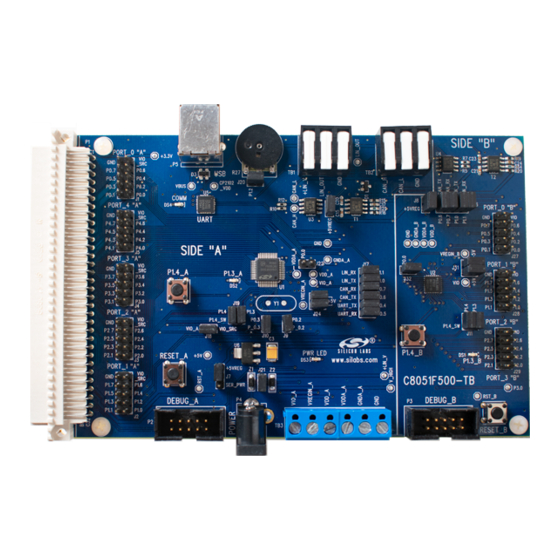
C8051F500DK 8. Target Board The C8051F500 Development Kit includes a target board with a C8051F500 (Side A) and C8051F502 (Side B) device pre-installed for evaluation and preliminary software development. Numerous input/output (I/O) connections are provided to facilitate prototyping using the target board. Refer to Figure 3 for the locations of the various I/O connectors. - Page 8 F500 Port 3 “A” Port 1 “B” P1.4_A F502 Port 2 “A” Port 2 “B” J10 J9 P1.4_B P1.3_B SILICON LABS www.silabs.com RESET_A C8051F500-TB Port 1 “A” DEBUG_A DEBUG_B RESET_B Figure 3. C8051F500 Target Board with Pin Numbers Rev. 0.1...
- Page 9 C8051F500DK 8.1. Target Board Shorting Blocks: Factory Defaults The C8051F500 target board comes from the factory with pre-installed shorting blocks on many headers. Figure 4 shows the positions of the factory default shorting blocks. Port 0 “A” SIDE “B” COMM Port 0 “B”...
- Page 10 The on-chip crystal is accurate for CAN and LIN master communications and in many applications an external oscillator is not required. However, if you wish to operate the C8051F500 device (SIDE A) at a frequency not available with the internal oscillator, an external crystal may be used. Refer to the C8051F50x data sheet for more information on configuring the system clock source.
- Page 11 The second red LED labeled COMM indicates if the CP2102 USB-to-UART bridge (P5) is recognized by the PC. The green LED labeled with port pin name P1.3_A is connected to the C8051F500’s (Side A) GPIO pin P1.3 through the header J19. Remove the shorting block from the header to disconnect the LED from the port pin.
- Page 12 UART0 of the C8051F500 (Side A). The Silicon Labs CP2102 USB-to-UART bridge provides data connectivity between the C8051F500 and the PC via a USB port. The TX and RX signals of UART0 may be connected to the CP2102 by installing shorting blocks on header J17. The shorting block positions for connecting each of these signals to the CP2102 are listed in Table 3.
- Page 13 8.9. Port I/O Connectors (J1-J5 and J27-J29) Each of the parallel ports of the C8051F500 (Side A) and C8051F502 (Side B) has its own 10-pin header connector. Each connector provides a pin for the corresponding port pins 0-7, +5V VIO, and digital ground. The same pin-out is used for all of the port connectors.
- Page 14 The 96-pin expansion I/O connector P1 is used to connect daughter boards to the main target board. P1 provides access to many C8051F500 signal pins. Pins for VREGIN, VDD, VIO, and 3.3V are also available. See Table 9 for a complete list of pins available at P1.
- Page 15 (ADC) converter of the MCU. 8.13. Power Supply I/O (Side A) (TB3) All of the C8051F500 target device’s supply pins are connected to the TB3 terminal block. Refer to Table 10 for the TB3 terminal block connections. Table 10. TB1 Terminal Block Pin Descriptions...
- Page 16 Some GPIO pins of the C8051F500 MCU can have an alternate fixed function. For example, pin 46 on the C8051F500 MCU is designated P0.4, and can be used as a GPIO pin. Also, if the UART0 peripheral on the MCU is enabled using the crossbar registers, the TX signal is routed to this pin.
- Page 17 C8051F500DK Table 11. C8051F500 Target Board Pin Assignments and Headers (Continued) P3.2 P3.2 GPIO J4[3] P3.3 P3.3 GPIO J4[4] P3.4 P3.4 GPIO J45] P3.5 P3.5 GPIO J4[6] P3.6 P3.6 GPIO J4[7] P3.7 P3.7 GPIO J4[8] P4.0 P4.0 GPIO J5[1] P4.1 P4.1...
- Page 18 C8051F500DK 9. Schematics Rev. 0.1...
- Page 19 C8051F500DK Rev. 0.1...
- Page 20 C8051F500DK Rev. 0.1...
- Page 21 C8051F500DK Rev. 0.1...
-
Page 22: Contact Information
Silicon Laboratories products are not designed, intended, or authorized for use in applications intended to support or sustain life, or for any other application in which the failure of the Silicon Laboratories product could create a situation where per- sonal injury or death may occur.
Need help?
Do you have a question about the C8051F500 and is the answer not in the manual?
Questions and answers