Advertisement
Quick Links
C8051F930 D
1. Relevant Devices
The C8051F930 Development Kit is intended as a development platform for the microcontrollers in the
C8051F93x-C8051F92x MCU family.
Notes:
1. The target board included in this kit is provided with a pre-soldered C8051F930 MCU (LQFP32 package).
2. Code developed on the C8051F930 can be easily ported to the other members of this MCU family.
3. Refer to the C8051F93x-C8051F92x data sheet for the differences between the members of this MCU
family.
2. Kit Contents
The C8051F930 Development Kit contains the following items:
C8051F930 Target Board
C8051Fxxx Development Kit Quick-Start Guide
AC to DC Power Adapter
USB Debug Adapter (USB to Debug Interface)
2 USB Cables
2 AAA Batteries
CD-ROM
Rev 0.7 5/14
EVELOPMENT
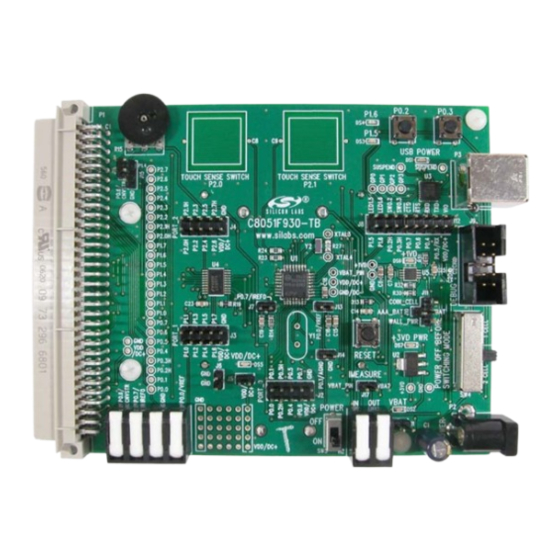
Figure 1. C8051F930 Target Board
Copyright © 2014 by Silicon Laboratories
C 8 0 5 1 F 9 3 x / 9 2 x
K
U
'
G
IT
S E R
S
UIDE
C8051F93x/92x
Advertisement

Related Manuals for Silicon Laboratories C8051F93 Series


Summary of Contents for Silicon Laboratories C8051F93 Series
- Page 1 C8051Fxxx Development Kit Quick-Start Guide AC to DC Power Adapter USB Debug Adapter (USB to Debug Interface) 2 USB Cables 2 AAA Batteries CD-ROM Figure 1. C8051F930 Target Board Rev 0.7 5/14 Copyright © 2014 by Silicon Laboratories C8051F93x/92x...
-
Page 2: Hardware Setup Using A Usb Debug Adapter
C8051F93x/92x 3. Hardware Setup Using a USB Debug Adapter The target board is connected to a PC running the Silicon Laboratories IDE via the USB Debug Adapter as shown in Figure 2. 1. Connect the USB Debug Adapter to the DEBUG connector on the target board with the 10-pin ribbon cable. -
Page 3: Software Setup
C8051F93x/92x 4. Software Setup Simplicity Studio greatly reduces development time and complexity with Silicon Labs EFM32 and 8051 MCU products by providing a high-powered IDE, tools for hardware configuration, and links to helpful resources, all in one place. Once Simplicity Studio is installed, the application itself can be used to install additional software and documentation components to aid in the development and evaluation process. - Page 4 C8051F93x/92x 4.1. Running Blinky Each project has its own source files, target configuration, SDK configuration, and build configurations such as the Debug and Release build configurations. The IDE can be used to manage multiple projects in a collection called a workspace.
- Page 5 C8051F93x/92x 4.3. Simplicity Configurator The Simplicity Configurator is a configuration and code generation tool. This utility helps accelerate development by automatically generating initialization source code to configure and enable the on-chip resources needed by most design projects. In just a few steps, the wizard creates complete startup code for a specific Silicon Labs MCU. To create a new Simplicity Configurator project: ...
- Page 6 C8051F93x/92x To configure pins, click on the DefaultMode Port I/O tab at the bottom of main window. Clicking on a pin brings up a property window for the pin. Clicking anywhere else in the main window opens a property window for the crossbar.
- Page 7 C8051F93x/92x 4.4. CP210x USB to UART VCP Driver Installation The MCU Card includes a Silicon Labs CP210x USB-to-UART Bridge Controller. Device drivers for the CP210x need to be installed before the PC software can communicate with the MCU through the UART interface. Use the drivers included CD-ROM or download the latest drivers from the website (www.silabs.com/interface-software).
- Page 8 C8051F93x/92x 4.5. Silicon Labs Battery Life Estimator The Battery Life Estimator is a system design tool for battery operated devices. It allows the user to select the type of battery they are using in the system and enter the supply current profile of their application. Using this information, it performs a simulation and provides an estimated system operating time.
- Page 9 C8051F93x/92x Figure 7. Battery Life Estimator Discharge Profile Editor The Discharge Profile Editor allows the user to modify the profile name and description. The four text entry boxes on the left hand side of the form allow the user to specify the amount of time the system spends in each power mode.
- Page 10 C8051F93x/92x The wakeup frequency box calculates the period of a single iteration through the four power modes and displays the system wake up frequency. This is typically the "sample rate" in low power analog sensors. Once the battery type and discharge profile is specified, the user can click the "Simulate" button to start a new simulation.
-
Page 11: Target Board
C8051F93x/92x 5. Target Board The C8051F930 Development Kit includes a target board with a C8051F930 device pre-installed for evaluation and preliminary software development. Numerous input/output (I/O) connections are provided to facilitate prototyping using the target board. Refer to Figure 9 for the locations of the various I/O connectors. Figure 11 on page 13 shows the factory default shorting block positions. - Page 12 C8051F93x/92x The following items are located on the bottom side of the board. See Figure 10. BT1 Battery Holder for 1.5 V AAA. Use for one-cell or two-cell mode. BT2 Battery Holder for 1.5 V AAA. Use for two-cell mode only. BT3 Battery Holder for 3 V Coin Cell (CR2032).
- Page 13 C8051F93x/92x 5.1. Target Board Shorting Blocks: Factory Defaults The C8051F930 target board comes from the factory with pre-installed shorting blocks on many headers. Figure 11 shows the positions of the factory default shorting blocks. P1.6 P0.2 P0.3 P1.5 P1.4 USB POWER TOUCH SENSE SWITCH TOUCH SENSE SWITCH P2.0...
- Page 14 C8051F93x/92x 5.2. Target Board Power Options and Current Measurement The C8051F930 Target Board supports three power options, selectable by the three-way header (J10/J11). The power options vary based on the configuration (one-cell or two-cell mode) selected by SW4. Power to the MCU may be switched on/off using the power switch (SW5).
- Page 15 C8051F93x/92x 5.3. System Clock Sources 5.3.1. Internal Oscillators The C8051F930 device installed on the target board features a factory calibrated programmable high-frequency internal oscillator (24.5 MHz base frequency, ±2%) and a low power internal oscillator (20 MHz ±10%). After each reset, the low power oscillator divided by 8 results in a default system clock frequency of 2.5 MHz (±10%).
- Page 16 C8051F93x/92x 5.5. Switches and LEDs Three push-button switches are provided on the target board. Switch SW1 is connected to the reset pin of the C8051F930. Pressing SW1 puts the device into its hardware-reset state. Switches SW2 and SW3 are connected to the C8051F930’s general purpose I/O (GPIO) pins through headers.
- Page 17 C8051F93x/92x 5.6. Expansion I/O Connector (P1) The 96-pin Expansion I/O connector P1 provides access to all signal pins of the C8051F930 device (except the C2 debug interface signals). In addition, power supply and ground pins are included. A small through-hole prototyping area is also provided.
- Page 18 C8051F93x/92x 5.7. Target Board DEBUG Interface (J9) The DEBUG connector J9 provides access to the DEBUG (C2) pins of the C8051F930. It is used to connect the Serial Adapter or the USB Debug Adapter to the target board for in-circuit debugging and Flash programming. Table 3 shows the DEBUG pin definitions.
- Page 19 C8051F93x/92x 5.10. IREF Connector (J7) The C8051F930 Target Board also features a current-to-voltage 1 k load resistor that may be connected to the current reference (IREF0) output that can be enabled on port pin (P0.7). Install a shorting block on J7 to connect port pin P0.7 of the target device to the load resistor.
-
Page 20: Frequently Asked Questions
C8051F93x/92x 6. Frequently Asked Questions 1. Should power be turned off when switching between one-cell and two-cell mode? Yes, power must be turned off by placing SW5 in the OFF position when switching between one-cell and two-cell mode. Switching between modes while power is on may result in increased power consumption and possible damage to low voltage transistors. - Page 21 C8051F93x/92x 6. What can I do to reduce active supply current? Below are some suggestions for reducing the active supply current: a. Clear all wake-up sources in the PCU0CF register. This will allow the low power oscillator to be disabled when it is not being used as the system clock. This optimization can reduce the supply current by up to 30 µA.
- Page 22 C8051F93x/92x 11. When the missing clock detector is enabled, why does the MCU reset if I switch from the default system clock (Low Power Oscillator divided by 8) to smaRTClock divided by 1? Background: —The missing clock detector will trigger a reset if the system clock period exceeds 100 µs. —Switchover between clock sources occurs in 1 clock cycle of the slowest clock.
- Page 23 C8051F93x/92x 7. Schematics Rev 0.7...
- Page 24 C8051F93x/92x Rev 0.7...
- Page 25 C8051F93x/92x Rev 0.7...
- Page 26 The products must not be used within any Life Support System without the specific written consent of Silicon Laboratories. A "Life Support System" is any product or system intended to support or sustain life and/or health, which, if it fails, can be reasonably expected to result in significant personal injury or death.
- Page 27 Mouser Electronics Authorized Distributor Click to View Pricing, Inventory, Delivery & Lifecycle Information: Silicon Laboratories C8051F930DK...
Need help?
Do you have a question about the C8051F93 Series and is the answer not in the manual?
Questions and answers