
Related Manuals for AXIOMTEK sbc84500


Summary of Contents for AXIOMTEK sbc84500
- Page 1 SBC84500 Series 3.5” HDD Form Factor SBC with CRT/TFT/AUDIO and Fast Ethernet User’s Manual...
- Page 2 AXIOMTEK assumes no responsibility for any inaccuracies that may be contained in this document. AXIOMTEK makes no commitment to update or to keep current the information contained in this manual.
-
Page 3: Table Of Contents
Table of Contents Chapter 1 Introduction ..............1 1.1 General Description ............1 1.2 Specifications ..............2 Chapter 2 Installation ..............5 2.1 Board Dimension and Fixing Holes........5 2.2 Placement................6 2.3 Jumper Settings ..............7 2.3.1 Watchdog Function Setting: JP1............7 2.3.2 Serial Ports Settings: JP9, JP10, JP11 ..........8 2.3.3 CMOS Clear Jumper: JP8.............. - Page 4 3.19 IrDA Connector ..............25 3.20 Power Input Connectors ..........25 3.21 PC/104 Connectors............26 3.22 HDD LED Connector............28 3.23 Power LED Connector.............28 3.24 Hardware Reset Connector ..........28 3.25 Audio Connector..............28 Chapter 4 Display Drivers ............29 4.1 Introduction................29 4.1.1 Chipset ....................29 4.1.2 Display memory................29 4.2 Installation of SVGA driver ..........30 4.2.1 Installation for National MediaGX Certified drivers for Windows 95/98.
- Page 5 This page does not contain any information. Table of Contents...
-
Page 7: Chapter 1 Introduction
C h a p t e r Introduction General Description AXIOMTEK new SBC84500 NS Geode Series is a 3.5" SBC which offers an onboard NS Geode GX1-233 processor, plus support for Ethernet network functions onboard features include VGA/TFT LCD, a Compact-Flash™ card socket, and watchdog timer. -
Page 8: Specifications
SBC84500 User’s Manual Specifications Process: 233MHz National Semiconductor Geode GX1 (other frequency processors are manufacturer optional) Chipset: NS GX1 + CS5530A Memory: 1x144-pin SODIMM Max. 256MB SDRAM (Please refer to Appendix C for more information.) On-board IDE: PIO Mode 0-4, DMA Mode 0-1 and One... - Page 9 SBC84500 User’s Manual BIOS: AWARD BIOS with DMI, Plug-and-Play & Y2K Compliant in 2Mbit Flash Rom SmartView VGA BIOS Function Integration Ethernet Novell Boot Rom Function RTC: Integration in W83977AF with external Lithium Battery On-Board Display: CS5530A South Bridge Integrated Support CRT/TFT Display via UMA Max.
- Page 10 SBC84500 User’s Manual This page does not contain any information. Introduction...
-
Page 11: Chapter 2 Installation
SBC84500 User’s Manual C h a p t e r Installation Board Dimension and Fixing Holes 104.64 98.37 93.59 17.39 4.83 3.18 0.00 Unit:mm Installation... -
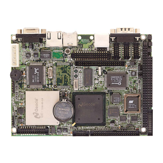
Page 12: Placement
SBC84500 User’s Manual Placement LCD1 CON1 IDE1 JP10 JP16 FDD1 LAN1 USB2 KBMS1 VGA1 COM1 SODIMM1 Installation... -
Page 13: Jumper Settings
SBC84500 User’s Manual Jumper Settings The SBC84500VEA is configured to match the needs of your application by proper jumper settings. The following tables show the correct jumper settings for the onboard devices. Jumper Default Setting Jumper Setting Watchdog Trigger Disabled... -
Page 14: Serial Ports Settings: Jp9, Jp10, Jp11
SBC84500 User’s Manual 2.3.2 Serial Ports Settings: JP9, JP10, JP11 The SBC84500VEA provides 4 onboard serial ports, 3 x RS-232 and 1 x RS-232/422/485. The corresponding jumper settings are shown on the following table. If COM2 is to be set to RS-422/485, the following jumpers have to be set correctly. -
Page 15: Serial Ports +5V And +12V Power Selection: Jp13, Jp15, Jp14, Jp16
SBC84500 User’s Manual 2.3.6 Serial Ports +5V and +12V Power Selection: JP13, JP15, JP14, JP16 The four COM ports have +5V/+12V power capability on Pin 1 (+5V) and Pin 8 (+12V) or Pin 9 (+12V), depending on the jumper selection. The RS-232’s pin assignments are listed. -
Page 16: Connectors
SBC84500 User’s Manual Connectors The onboard connectors link the SBC84500VEA to external devices such as hard disk, floppy disk or printer. The following table lists the function of each connector on the SBC84500VEA. Corresponding pin assignments are described in Chapter 3. -
Page 17: Chapter 3 Hardward Description
SBC84500 User’s Manual C h a p t e r Hardware Description Safety Precaution Disconnect the power cord from the SBC84500VEA before your installation. Do not make any connections while the power is on because the sudden surge of power could ruin any sensitive components. Most electronic components are sensitive to the static electric charge. -
Page 18: System Memory
SBC84500 User’s Manual System Memory SBC84500VEA has one onboard 144-pin SODIMM sockets, able to support 16MB, 32MB, 64MB, 128MB SODIMM modules, providing the user with up to 128MB system memory. Interrupt Controller The SBC84500VEA is a fully PC compatible control board. It consists of 16 ISA interrupt request lines and 4 of the 16 can be either ISA or PCI. -
Page 19: System I/O Address Map
SBC84500 User’s Manual System I/O Address Map Address Map Description 000-01F DMA Controller #1 020-021 Interrupt Controller # 1, Master 022-023 Chipset address 040-05F System Timer 060-06F Standard 101/102 keyboard Controller 070-07F Real time Clock, NMI Controller 080-0BF DMA Page Register... -
Page 20: Dma Channel Assignments
SBC84500 User’s Manual DMA channel assignments Channel Function Available Available Floppy disk (8-bit transfer) Parallel** Cascade for DMA controller 1 Available Available Available Hardware Description... -
Page 21: Ide Interface Connector
SBC84500 User’s Manual IDE Interface Connector The SBC84500VEA builds in 1 channel, able to support 2 IDE drives, PCI bus enhanced IDE controller which can support master/slave mode and post write transaction mechanisms with 64-byte buffer, and master data transaction. -
Page 22: Compactflash™ Socket (U25)
SBC84500 User’s Manual CompactFlash™ Socket (U25) The SBC84500VEA Series is equipped with a CompactFlash disk socket on the solder side and it supports the IDE interface CompactFlash disk card. The socket itself is especially designed to prevent any incorrect installation of the CompactFlash disk card. -
Page 23: Vga/Flat Panel Connectors
SBC84500 User’s Manual 3.10.2 VGA/Flat Panel Connectors The SBC84500VEA has two connectors to support the CRT VGA and flat panel displays, respectively or simultaneously. VGA1 is a standard 15-pin connector commonly used for the CRT VGA display, and LCD1 is a 44-pin, dual-in-line header for flat panel connection. -
Page 24: Flat Panel Connector Pin Description
SBC84500 User’s Manual Description Description G4 (P14) G5 (P15) No connector No connector R0 (P18) R1 (P19) R2 (P20) R3 (P21) R4 (P22) R5 (P23) FPCLK FPVSYNC (FLM) FPDISP FPHSYNC (LP) FPENABKL No connector No connector VDDM 3.10.3 Flat Panel Connector Pin Description... -
Page 25: Floppy Disk Controller
SBC84500 User’s Manual 3.11 Floppy Disk Controller The SBC84500VEA provides a 34-pin header type connector, FDD1 for supporting up to two floppy drives. The floppy drives could be any one of the following types: 3.5" /1.44MB/2.88MB. FDD1: Floppy Disk Connector Pin Assignment... -
Page 26: Digital I/Os
SBC84500 User’s Manual 3.12 Digital I/Os The board is equipped with a 8-channel digital I/O connector CN1 that meets a system’s customary automation control needs. The digital I/O can be configured to control the cash drawer, or to sense the warning signal of an Uninterrupted Power System (UPS), or to perform the store security control. -
Page 27: Digital I/O Software Programming
SBC84500 User’s Manual 3.12.1 Digital I/O Software Programming The Digital I/O on the the board is not an isolated type. Output Address Bit Output Address Bit Out-0 123h In-0 123h Out-1 123h In-1 123h Out-2 123h In-2 123h Out-3 123h... -
Page 28: Parallel Port Interface
SBC84500 User’s Manual 3.13 Parallel Port Interface The onboard PRT of SBC84500VEA is a multi-mode parallel port able to support: Standard mode: IBM PC/XT, PC/AT and PS/2 compatible with bi-directional parallel port Enhanced mode: Enhance parallel port (EPP) compatible with EPP 1.7 and EPP 1.9 (IEEE 1284 compliant) -
Page 29: Serial Port Interface
SBC84500 User’s Manual 3.14 Serial Port Interface The SBC84500VEA has four onboard serial ports, with COM1,COM3,COM4 as RS-232 and COM2 as RS-232/422/485, both selected via jumper setting. Both ports have +5V/12V power on pins 1 (+5V) and 8 or pin 9 (+12V), depending on jumper selection. The RS-232’s pin assignments are listed below;... -
Page 30: Usb Connector
SBC84500 User’s Manual 3.15 USB Connector There are two USB connectors allow installation of USB devices. USB1 is a single standard USB connector. USB1 is 4-pin header connector. The following table shows the pin outs of the USB connector. Pin #... -
Page 31: Ethernet Connector
SBC84500 User’s Manual 3.18 Ethernet Connector The RJ-45 connector (Lan1 ) is used for Ethernet. To connect the SBC84500VEA to a hub, just plug one end of the cable into the Lan1 and connect the other end of the cable to a hub. -
Page 32: Pc/104 Connectors
SBC84500 User’s Manual 3.21 PC/104 Connectors The PC/104 is an industrial standard. It is a compact form factor of the dimension of 3.6” x 3.8” and is fully compatible with the ISA Bus. The PC/104 interface is able to adapt the off-shelf PC/104 modules, such as sound module, fax modem module and multi-I/O module…etc. - Page 33 SBC84500 User’s Manual PIN No. PIN Name PIN No. PIN Name IRQ3 DACK2 * SALE PC104-2: PC/104 Bus Pin Assignments PIN No. PIN Name PIN No. PIN Name MEMCS16 * SBHE * IOCS16 * LA23 IRQ10 LA22 IRQ11 LA21 IRQ12...
-
Page 34: Hdd Led Connector
SBC84500 User’s Manual 3.22 HDD LED Connector JP7: 2 Pin connector for HDD LED communication. Description LED+ LED- 3.23 Power LED Connector JP6: 2 Pin connector for Power LED communication. Description LED+ LED- 3.24 Hardware Reset Connector JP4: 2 Pin connector for Hardware Reset communication. -
Page 35: Chapter 4 Display Drivers
SBC84500 User’s Manual C h a p t e r Display Drivers Introduction The SBC84500VEA Series has an on-board LCD/VGA interface. The specifications and features are described as follows: 4.1.1 Chipset The SBC84500VEA uses a NS CS5530A chipset for its SVGA controller. -
Page 36: Installation Of Svga Driver
Complete the following steps to install the SVGA driver. Follow the procedures in the flow chart that apply to the operating system that you are using within your SBC84500. Important: The following windows illustrations are examples only. You must follow the flow chart instructions and pay attention to the instructions which then appear on your screen. -
Page 37: Chapter 5 Ethernet Introduction
SBC84500 User’s Manual C h a p t e r Ethernet Introduction Introduction The SBC84500VEA is equipped with a high performance Plug and Play Ethernet interface which is fully compliant with the IEEE 802.3 standard, and consisting of a RJ-45 connector Lan1. - Page 38 SBC84500 User’s Manual This page does not contain any information. Ethernet Introduction...
-
Page 39: Chapter 6 Award Bios Utility
3. The CMOS memory has lost power and the configuration information has been erased. The SBC84500 Series' CMOS memory has an integral lithium battery backup. The battery backup should last ten years in normal service, but when it finally runs down, you will need to replace the complete unit. -
Page 40: Entering Setup
SBC84500 User’s Manual 6.2.1 Entering setup Power on the computer and press <Del> immediately. This will allow you to enter Setup. ROM PCI/ISA BIOS (SBC84500) CMOS SETUP UTILITY AWARD SOFTWARE, INC. STANDARD CMOS SETUP INTEGRATED PERIPHERALS BIOS FEATURES SETUP SUPERVISOR PASSWORD... -
Page 41: Standard Cmos Setup
The Standard CMOS Setup is used for basic hardware system configuration. The main function is for Date/Time setting and Floppy/Hard Disk Drive setting. Please refer the following screen for this setup. ROM PCI/ISA BIOS (SBC84500) STANDARD CMOS SETUP AWARD SOFTWARE, INC. -
Page 42: Bios Features Setup
This BIOS Features Setup is designed for the 'fine tuning' of your system in order to improve its performance. As for normal operation, you don‘t have to change any default setting. The default setting is pre-set for most reliable operation. ROM PCI/ISA BIOS (SBC84500) BIOS FEATURES SETUP AWARD SOFTWARE, INC. Virus Warning... -
Page 43: Chipset Features Setup
This setup function works mostly on board's chipset. This option is used to change the chipset's configuration. Please, carefully change any default setting, otherwise the system will run unstable. ROM PCI/ISA BIOS (SBC84500) CHIPSET FEATURES SETUP AWARD SOFTWARE, INC. SDRAM CAS lantency TIme... -
Page 44: Power Management Setup
SBC84500 User’s Manual 6.2.5 Power management setup Power Management Setup helps user to handle the SBC84500 board‘s “green” function. This feature can shut down the video display and hard disk to save energy, for example. The power management setup screen is as following. -
Page 45: Pnp/Pci Configuration
SBC84500 User’s Manual 6.2.6 PnP/PCI configuration This menu is used to assign certain IRQ to your PNP/PCI Devices manually. ROM PCI/ISA BIOS (SBC84500) PNP/PCI CONFIGURATION AWARD SOFTWARE, INC. PNP OS Installed : No PCI IRQ Actived By : Level Resources Controlled By... -
Page 46: Integrated Peripherals
SETUP SCREEN menu, the screen below is displayed. This sample screen contains the manufacturer’s default values for the SBC84500VEA Series. The PANEL TYPE by default supports a 18-bit 640 x 480 TFT LCD panel display. ROM PCI/ISA BIOS (SBC84500) INTEGRATED PERIPHERALS AWARD SOFTWARE, INC. IDE HDD Block Mode... - Page 47 SBC84500 User’s Manual Audio IRQ Select -- 5, 7, 10, Disabled To select the interrupt for audio function. Audio Low DMA Select -- DMA0, DMA1, DMA3, Disabled To select the high DMA channel. Audio High DMA Select -- DMA5, DMA6, DMA7, Disabled To select the high DMA channel.
-
Page 48: Load Bios Defaults
Suggestion: for the first time or for our primary user, we suggest you to use LOAD SETUP DEFAULTS because it is the safest mode for your system. ROM PCI/ISA BIOS (SBC84500) CMOS SETUP UTILITY AWARD SOFTWARE, INC. STANDARD CMOS SETUP... -
Page 49: Load Setup Defaults
If you select 'Y' to this field, the Setup Defaults will be loaded except Standard CMOS SETUP. The default settings are optimal configuration settings for your system. ROM PCI/ISA BIOS (SBC84500) CMOS SETUP UTILITY AWARD SOFTWARE, INC. STANDARD CMOS SETUP... -
Page 50: Auto Detect Hard Disk
Standard CMOS Setup screen. Up to 2 IDE drives can be detected and the parameters will be listed in the box. Press <Y> if you accept these parameters. Press <N> to skip the next IDE drives. ROM PCI/ISA BIOS (SBC84500) CMOS SETUP UTILITY AWARD SOFTWARE, INC. -
Page 51: Save & Exit Setup
This record is required for the system to operate. ROM PCI/ISA BIOS (SBC84500) CMOS SETUP UTILITY AWARD SOFTWARE, INC. - Page 52 SBC84500 User’s Manual This page does not contain any information. Award BIOS Utility...
-
Page 53: Appendix A Watchdog Timer
SBC84500 User’s Manual A p p e n d i x Watchdog Timer Using the Watchdog Function The SBC84500VEA CPU card uses version 2.0 of the watchdog timer. This onboard WDT generates either a system reset , depending on the settings made on jumper JP1 of SBC84500VEA. - Page 54 SBC84500 User’s Manual 0.5 sec. 5 secs. 50 secs. 100 secs. 1 sec. 10 secs. 100 secs. 200 secs. 1.5 secs. 15 secs. 150 secs. 300 secs. 2 secs. 20 secs. 200 secs. 400 secs. 2.5 secs. 25 secs. 250 secs.
-
Page 55: Appendix B Electrical Power Requirements
NEC 128MB(SODIMM) CPU Usage 100%(GX1-233Mhz) Memory Usage >80% Active Devices Lan, Video, Audio, COM1~COM4, LPT, IDE, FDD 3.Test condition: (1)room temp (2)Maxpow ,Windows98 4. SBC84500 Test Result Summary: Suggest Power Supply Item Amp(a) Pow(w) (Min Watt) GX1-233MHZ 1.31A 6.55W 9.17W(min) GX1-300MHZ 1.54A... - Page 56 SBC84500 User’s Manual This page does not contain any information. Electrical Power Requirements...
-
Page 57: Appendix C So-Dimm Used Notice
SBC84500 User’s Manual A p p e n d i x SO-DIMM Used Notice 1.PC SDRAM specification overview SDRAM (4Mx16, 8Mx16, 8Mx8, 16Mx8, 16Mx4 chips Package) memory address from A0 to A13 total 128M/bit support (SBC84500 can use) SO-DIMM Used Notice... - Page 58 SBC84500 User’s Manual SDRAM (16Mx16, 32Mx8, 64Mx4 chips Package) memory address from A0 to A14 total 256M/bit support (SBC84500 didn’t have address A14, only can detect only 128MB) SO-DIMM Used Notice...
- Page 59 SBC84500 User’s Manual 2.SBC84500 specification overview 1. memory address from A0 to A12 , SDRAM (4Mx16,8Mx16,8Mx8,16Mx8,16Mx4 chips Package) 2. total 256M/byte support ,you can use (Sixteen CMOS 16Mx8bit with 4banks SDRAMS or Sixteen CMOS 8Mx16bit with 4banks SDRAMS Thirty-two CMOS...
- Page 60 SBC84500 User’s Manual (SODIMM TOP side) (SODIMM Bottom side) SO-DIMM Used Notice...
Need help?
Do you have a question about the sbc84500 and is the answer not in the manual?
Questions and answers