Table of Contents
Advertisement
Service
Manual
REMARK : This service manual explains them by extracting specifications
designed for the model CDR631 only. The explanation for CD-R module
"MAR770" (Loader : CDL4009' + CD-R Main board) is not mentioned on this
service manual.
The CD-R module information is described in the service manual of CD-R
modules <MAR770/MAR775>.
SECTION
MAIN UNIT
1. Servicing the CDR631 ............................................................................................................................... 1
2. TECHNICAL SPECIFICATIONS ............................................................................................................... 3
3. WARNINGS .............................................................................................................................................. 4
4. SERVICE HINTS AND TOOLS ................................................................................................................. 5
5. DIAGNOSTIC SOFTWARE ....................................................................................................................... 6
6. FAULTFINDING TREES ......................................................................................................................... 10
7. FAULTFINDING GUIDE .......................................................................................................................... 14
8. WIRING DIAGRAM ................................................................................................................................. 29
9. BLOCK DIAGRAM ................................................................................................................................... 31
10. SCHEMATIC DIAGRAM AND PARTS LOCATION ................................................................................. 33
11. EXPLODED VIEW AND PARTS LIST ..................................................................................................... 43
12. ELECTRICAL PARTS LIST ..................................................................................................................... 46
Please use this service manual with referring to the user guide ( D.F.U. ) without fail.
Printed in Japan
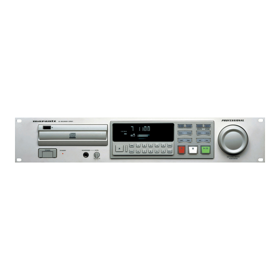
CD RECORDER CDR631
IR
Recordable
ReWritable
TIME
STANDBY
POWER
HEADPHONE
LEVEL
TEXT
0
10
TABLE OF CONTENTS
CDR631
CDR631 /
REC MODE
TR.INCR.
RANDOM
REPEAT
STORE
DELETE
FINAL
ERASE
CANCL
MENU
1
2
3
4
5
PROG
6
7
8
9
0
INPUT
REC LEVEL/SELECT
PUSH ENTER
F1B, /N1M, /U1B
CD Recorder
PAGE
R
387K855010 MIT
3120 785 22410
First Issue 2001.02
Advertisement
Table of Contents

Related Manuals for Marantz CDR631


Summary of Contents for Marantz CDR631
-
Page 1: Table Of Contents
REC LEVEL/SELECT PUSH ENTER REMARK : This service manual explains them by extracting specifications designed for the model CDR631 only. The explanation for CD-R module "MAR770" (Loader : CDL4009' + CD-R Main board) is not mentioned on this service manual. - Page 2 MARANTZ Parts for your equipment are generally available to our National Marantz Subsidiary or Agent. ORDERING PARTS : Parts can be ordered either by mail or by Fax.. In both cases, the correct part number has to be specified.
-
Page 3: Servicing The Cdr631
1.Servicing the CDR631 1.1 INTRODUCTION: The CDR631is the professional version of a CD recorder , this means that the SCMS (Serial Copy Management System) is not included. The CDR631can record on the Audio and CDRs PC. The CDR631is suitable for recording and playback of CD-R W discs (CD-Re Writable disc). - Page 4 1.2.2 Switching Power Supply Board. This PCB contains the Power Supply, which delivers the sevelal volteges for the each PCB in the CDR631. On this Power Supply a fuse (Primaly side) are mounted on this PCB. The power SW is jointed the Power bottom on the front panel.
-
Page 5: Technical Specifications
2 TECHNICAL SPECIFICATIONS GENERAL System ....................Compact disc digital audio Number of channels ................2 (stereo) Applicable discs ..................CD, CD-R , CD-RW Power Requirement F version ................... AC 100 V 50 / 60 Hz N version ................... AC 100 - 240 V 50 /60 Hz U version. -
Page 6: Warnings
3. WARNINGS WARNING WAARSCHUWING All ICs and many other semiconductors are susceptible to Alle IC´s en vele andere halfgeleiders zijn gevoelig voor electrostatic discharges (ESD). Careless handling during electrostatische ontladingen (ESD). repair can reduce life drastically. Onzorgvuldig behandelen tijdens reparatie kan de levensduur When repairing, make sure that you are connected with the drastisch doen vermindern. -
Page 7: Service Hints And Tools
4. SERVICE HINTS AND TOOLS SERVICE TOOLS “The tools listed below are standard test tools that can be used for repairing and testing Marantz CD Players & Recorders. Unless otherwise stated in the text, these tools are not mandatory for servicing Marantz CD Players &... -
Page 8: Diagnostic Software
5. Diagnostic Software Electrical service diagnostics ELECTRICAL SERVICE DIAGNOSTICS (software versions, test for defective components) If power ON, switch power OFF Load CD-DA disc (SBC444A) Press <PLAY> + <F FWD> simultaneously and switch ON unit LOADER TESTS PLAYER INFORMATION CDR LOADER TEST Display : ABORT TEST CD-DA disc must be loaded... - Page 9 5.1.1 Description Loader tests These tests determine if the CDR loader and the CD loader in case of a CDR500 work correctly. A CD-DA disc with a The intention of the electrical service diagnostics is to show the minimum of 3 tracks needs to be inserted in both loaders. A software versions present in the player and to direct the dealer disc test is executed to check focus control, disc motor control, towards defective internal units.
- Page 10 5.2 Mechanical service diagnostics MECHANICAL SERVICE DIAGNOSTICS (test for defective components) If power ON, switch power OFF Press <PLAY/PAUSE> + <STOP> simultaneously and switch ON unit < > OPEN TRAY TEST FOCUS TEST Visual inspection Display shows “BUSY” Display shows “OPENED” <...
- Page 11 5.3 DC-erase service mode DC ERASE SERVICE MODE (erasement of complete CD-RW) Load CD-RW disc Press <ERASE> + <RECORD> simultaneously and switch ON unit Display shows: “ ER mm:ss ” :remaining minutes :remaining seconds TOTAL and REM are also illuminated Display shows: “...
-
Page 12: Faultfinding Trees
6. Faultfinding Trees NO DISC LOADED SWITCH ON POWER PRESS <DISPLAY> CHECK: • MAINS, MAINS CABLE • POWER SUPPLY & TRAFO ⇒ WIRING ⇒ ON/OFF SWITCH ⇒ FUSES ⇒ VOLTAGES • DISPLAY (SEE FAULT FINDING GUIDE DISPLAY BOARD) DISPLAY? ⇒ WIRING ⇒... - Page 13 Faultfinding Trees CD-DA DISC LOADED CHECK: • WIRING DISC • POWER SUPPLY VOLTAGES DETECTION & READING? • ELECTRICAL SERVICE DIAGNOSTICS: REPLACE CDR MODULE IF "DERRn" OR "BERRn" ERROR OCCURS CHECK: DISPLAY: • DISC: DIRT, SCRATCHES, DAMAGED... “CD” & • ELECTRICAL SERVICE DIAGNOSTICS: T.O.C.
- Page 14 CD-R DISC LOADED CHECK: • DISC WIRING DETECTION & • POWER SUPPLY VOLTAGES READING? • ELECTRICAL SERVICE DIAGNOSTICS: REPLACE CDR MODULE IF "DERRn" OR "BERRn" ERROR OCCURS CHECK: DISPLAY: DISPLAY: • DISC: DIRT, SCRATCHES, DAMAGED... “CD R” & “CD” OR “CD R” & •...
- Page 15 CD-RW DISC LOADED CHECK: • DISC WIRING DETECTION & • POWER SUPPLY VOLTAGES READING? • ELECTRICAL SERVICE DIAGNOSTICS: REPLACE CDR MODULE IF "DERRn" OR "BERRn" ERROR OCCURS CHECK: DISPLAY: • DISPLAY: DISC: DIRT, SCRATCHES, DAMAGED... “CD RW” & “CD” OR “CD RW” & •...
-
Page 16: Faultfinding Guide
7. Faultfinding Guide 7.1 Display Board 7.1.1 Description of display board Display controller TMP87CH74F TMP87CH74F (QY01) is a high speed and high performance 8-bit single chip microprocessor, containing 8-bit A/D General description conversion inputs and a VFT (Vacuum Fluorescent Tube) The display board has three major parts : the FTD (Fluorescent driver. - Page 17 7.1.2 Test instructions Grid lines Level and timing of all grid lines, G1-->G15, can be checked either at the FTD itself or at the display controller. Grid lines Supply voltages G13, G14 and G15 each have an extra current amplifier in line The display board receives several voltages via connector : QY04 for G13, QY03 for G14 and QY02 for G15.
- Page 18 Figure 7-5 KEY MATRIX SCAN LINE IR receiver - remote control In the CDR631 the IR receiver ZY01 is mounted on the IR board. Easy jog knob In all versions the IR receiver connects to the display controller. The signal coming from the receiver can be checked at pin 22 of Rotary operation the display controller.
- Page 19 7.1.3 Display board troubleshooting guide SWITCH POWER ON, EXIT STAND BY MODE CHECK : • SUPPLY VOLTAGES ⇒ -34V ±5% at conn. JY52-2 ⇒ 4V3 ± 10% between conn. JY52-1 and JY52-3 DISPLAY? ⇒ +5V ± 5 % at conn. JY52-10 •...
-
Page 20: Block Diagram
7.2 Audio Board Pin description Pin Name PIN / FUNCTION The Audio board for the CDR631 is a full high performance AINR+ Right channel analog positive input pin AD/DA panel, acting as an interface to the outside world. Key AINR- Right channel analog negative input pin components are DS1807, ADC AK5351 and DAC AK4393. - Page 21 Addressable Dual Audio Taper Potentionmeter : DS1807 Block diagram Control Logic Address Logic Figure 7-12 Pin description DESCIPTION L0, L1 Low End of Resistor H0, H1 High End of Resistor W0,W1 Wiper Terminal of Resistor 3V/5V Power Supply Input A0..A2 Chip Select Inputs Serial Data I/O Serial Clock Input...
- Page 22 7.2.2 Analog-out path Description DAC AK4393 The I2S-bus data format being the digital output signal, goes Description from the DASP on the CDR main board via flex and connector The AK4393 is a high performance, single-chip stereo, audio J601 to the I/O board. Here it is presented to the D/A converter DAC delivering 101dB dynamic range sample rate.
- Page 23 Pin configuration and description No. Pin Name I/O Function DVSS Digital Ground Pin DVDD Digital Power Supply Pin, 3.3V or 5.0V MCLK Master Clock Input Pin Power-Down Mode Pin When at "L", the AK4393 is in power-down mode and is held in reset. The AK4393 should always be reset upon power-up.
- Page 24 Troubleshooting analog-out path LOAD SBC442 TEST CD (1kHz, -30dB) 4822 397 30155 CHECK: · Flex and wire connections +10V (QM01), -10V (QM02) · · CL11 = 11.2896MHz at pin 2 conn. J601 PRESS <PLAY> CHECK: KILL voltage testpoint 1 : -8V during play ·...
- Page 25 Power Supply Unit P816 cycle is regulated so that the output voltages are independent of load or input voltage variations. The controlling device MC44603 is an integrated pulse width modulator. A clock 7.4.1 Description of P816 signal initiates power pulses at a fixed frequency. The termination of each output pulse occurs when a feedback MOSFET Q825 is used as a power switch controlled by the signal of the inductor current reaches a threshold set by the...
- Page 26 Pin function description Name Description This pin is the positive supply of the IC. The operating voltage range after start-up is 9.0 to 14.5 V. The output high state (VOH) is set by the voltage applied to this pin. Output P eak currents up to 750 mA can be sourced or sunk, suitable for driving either MOSFET or bipolar transistors.
- Page 27 Block diagram of MC44603 Vref Iref Vref DEMAGNETISATION enable DETECT DEMAGNETISATION REFERENCE SUPPLY UVL01 MANAGEMENT BLOCK INITIALISATION BLOCK Iref VOSC PROT VOSC SYNC INPUT OSCILLATOR 1Set BUFFER LATCH RF STANDBY Vstby 1Reset STANDBY RP STANDBY (REDUCED FREQUENCY) 2.5V THERMAL SHUTDOWN Vref Iref VS8 OUT...
- Page 28 is switched off when the current sense level exceeds the level at the output of the error amplifier. TimeON phase : A drain current will flow from the positive CH1 2 supply at pin 2 of the transformer through the transformer's CH3 2 V~ ALT MTB5.00us- 0.90dv ch1- PM3394B primary winding, the MOSFET and Rsense to ground.
- Page 29 Circuit description of P816 Demagnetisation The auxiliary winding (7-9) voltage is used to detect magnetic saturation of the transformer core and connected via R801 to Input circuit pin 8 of Q810. During the demagnetisation phase, the output The input circuit consists of a lightning protection circuit and an will be disabled.
- Page 30 7.4.2 Troubleshooting P816 Check fuse F820 and replace if necessary Check DC voltages Power supply unit OK +5V, +12V, -8V, VFTD (-34V),VDC1-VDC2 (4V1) Disconnect power supply unit from CDR main board Connect dummy load resistors 10W, 15 ohm at +5V, +12V and ground Check DC voltages Power supply is OK +5V, +12V, -8V, VFTD, VDC1-VDC2...
- Page 31 8. WIRING DIAGRAM A : FFC 0.5mm F: PH-Bord-in 2.0mm 1 GND 1 IR_SENS 2 GND 2 SYS_CLK : CONNECTOR 3 +5V 3 n.c. 4 GND : BORD IN WIRE 5 IIS_WS_A0 MAINS G: PH-Bord in 2.0mm 6 IIS_BCK_A0 : from LOADER ASSY 1 STB_LED 7 GND 2 GND...
- Page 32 9. BLOCK DIAGRAM PP16 AUDIO PCB LOADER PCB COAXIAL DIG. DASP CDU4009 THROUGH DIG. COAXIAL DIG. XLR/COAXIAL OPT DIG. IN DEEMPH Driver MACE2 MUTE COAXIAL ANA. AK4393 Q601 OPT DIG. OUT INPUT SENS.VOL. XLR DIG. IN 0dBu ~ +22dBu EEPROM XLR ANA.
-
Page 33: Schematic Diagram And Parts Location
10. SCHEMATIC DIAGRAM AND PARTS LOCATION CB01 PP16 C707 470p 50V 470P +10VA C791 C711 47/16V 100p 50V C777 R775 R789 +5VADA +10VA 220/16V R751 C753 R755 4.7k R705 RB03 D701 47/16V 4.7k +5VADA C717 R711 1SS302(1) R723 R713 C725 CA03 CA08 CA07... - Page 34 SWITCHING POWER SUPPLY P816 Q851 L831 LM317 L854 µ L831 L853 D851 µ D802 Q892 AG01 C892 S1WB R853 PC123F 100/25 L825 D806 C819 C825 470pF R819 G815 C820 250V R852 C855 /400V 330k C827 C854 0.01 0.22 Q825 J801 (UL/CSA,MITI) 470pF C851...
- Page 35 PY16 PY26 DISPLAY SY01 SY02 SY03 SY05 SY06 SY04 VY01 PLAY STOP OPN/CLS PAUSE MODE FINAL KEY_OUTPUT4 SY07 SY08 SY10 SY11 SY12 VDC1 VFTD ERASE INPUT PROG RANDOM TIME KEY_OUTPUT3 DY04 3.3V SY13 SY14 SY63 SY64 VDC2 RY14 3.3K TEXT REPEAT KEY_OUTPUT2 SY22...
- Page 36 PP26 JT21 P816 CT21 J321 J761 J762 C763 C764 C761 C762 R321 Q829 Q815 Q825 R322 L753 L754 C324 R323 C323 Q817 Q862 Q861 Q819 Q801 Q810 R763 C769 R761 R764 C770 R762 J323 J711 PP26 C821 L820 D802 WG387K102-0 L831 Q892 L854...
- Page 37 PP16 QF51 QF52 Q761 Q763 Q762 Q764 Q331 QT31 QF332 Q326 QN53 QN51 QN54 QN52 QM04 QM23 QM24 Q703 Q705 Q701 Q702 Q704 Q706 Q603 Q604 Q601 QM06 QM03 QM07 Q615 Q707 QA01 QA02 Q708 Q661 Q662 Q663 Q665 Q666 QM21 QM22 Q664 QC01 PP16 WG387K101-0...
-
Page 38: Exploded View And Parts List
11. EXPLODED VIEW AND PARTS LIST 5 1 2 8 1 4 5 G 3 X 8 ( M) U, F ONLY 5 1 2 7 W0 0 1 5 1 2 7 N ONLY 3 X 8 ( M) 3 X 8 ( M) 5 1 2 7 5 1 2 8... - Page 39 VERS. PART NO. VERS. POS. POS. PART NO. PART NO. PART NO. DESCRIPTION DESCRIPTION COLOR COLOR (FOR PCS) (FOR PCS) (MJI) (MJI) 001B BLACK FRONT PANEL BLACK 387K248010 001M MECHANISM CD-R MODULE 387K304500 001B GRAY 9965 000 07404 FRONT PANEL GRAY 387K248110 MAR770 SPICE 2.08+ 003B BLACK...
-
Page 40: Electrical Parts List
12. ELECTRICAL PARTS LIST NOTE ON SAFETY FOR FUSIBLE RESISTOR : ASSIGNMENT OF COMMON PARTS CODES. RESISTORS The suppliers and their type numbers of fusible resistors : 1) GD05 × × × 140, Carbon film fixed resistor, ±5% 1/4W are as follows; : 2) GD05 ×... - Page 41 VERS. PART NO. VERS. POS. POS. PART NO. PART NO. PART NO. DESCRIPTION DESCRIPTION COLOR COLOR (FOR PCS) (FOR PCS) (MJI) (MJI) P816-SUPPLY R885 4822 050 26811 681Ω ±1% 1/6W GM11668100 CIRCUIT BOARD R895 JUMPER 75060501P0 P816-CAPACITORS C801 4822 122 31237 CER. 82pF J CH 50V BLK DD15820300 P816-RESISTORS (COMMON) C810...
- Page 42 VERS. PART NO. VERS. POS. POS. PART NO. PART NO. PART NO. DESCRIPTION DESCRIPTION COLOR COLOR (FOR PCS) (FOR PCS) (MJI) (MJI) S815 9965 000 05921 PUSH SWITCH SP01012480 CM22 4822 126 11687 CER. CHIP 0.1µF +80%-20% DK98104200 ESB92S94B TV-5 1.5MM CT01 4822 126 12339 CER.
- Page 43 VERS. PART NO. VERS. POS. POS. PART NO. PART NO. PART NO. DESCRIPTION DESCRIPTION COLOR COLOR (FOR PCS) (FOR PCS) (MJI) (MJI) C717 4822 124 41539 ELECT. 47µF M 16V RA-2 OA47601620 R621 C718 4822 124 41539 ELECT. 47µF M 16V RA-2 OA47601620 4822 051 30472 CHIP 4.7kΩ...
- Page 44 VERS. PART NO. VERS. POS. POS. PART NO. PART NO. PART NO. DESCRIPTION DESCRIPTION COLOR COLOR (FOR PCS) (FOR PCS) (MJI) (MJI) R743 4822 051 30102 CHIP 1kΩ ±5% 1/16W NN05102610 Q603 4822 209 17155 IC NJM2068MY HC10102090 R744 4822 051 30102 CHIP 1kΩ ±5% 1/16W NN05102610 Q604 4822 209 17155 IC NJM2068MY...
- Page 45 VERS. PART NO. VERS. POS. POS. PART NO. PART NO. PART NO. DESCRIPTION DESCRIPTION COLOR COLOR (FOR PCS) (FOR PCS) (MJI) (MJI) PP26-RESISTORS PY16-MISCELLANEOUS R321 4822 051 30331 CHIP 330Ω ±5% 1/16W NN05331610 LY01 482215753873 CHIP INDUCTANCE LU12104010 R322 4822 051 30331 CHIP 330Ω ±5% 1/16W NN05331610 NL322522-101K R323...
Need help?
Do you have a question about the CDR631 and is the answer not in the manual?
Questions and answers