
Subscribe to Our Youtube Channel
Related Manuals for Marantz CDR420/U1B


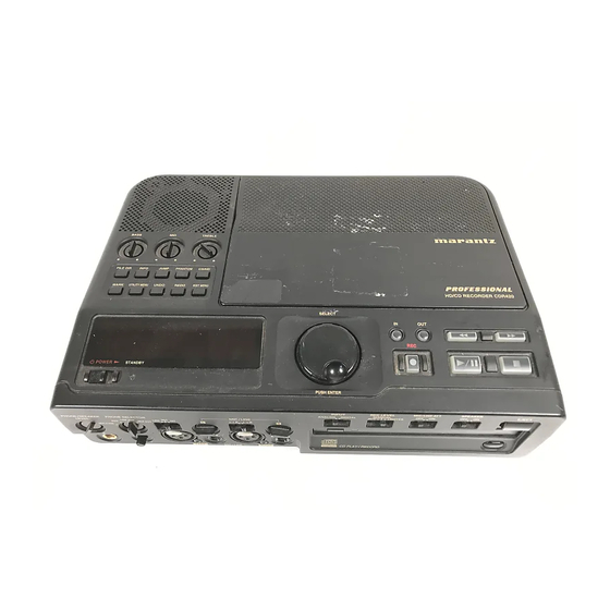
Summary of Contents for Marantz CDR420/U1B
- Page 1 Service CDR420/U1B Manual Please use this service manual in conjunction with the user guide ( D.F.U. ). CDR420/U1B Part no. 90M19AK855020 (99-20-420S) Revised 2005.10...
-
Page 2: Table Of Contents
TABLE OF CONTENTS SECTION PAGE 1. Specifications ………………………………………………………………………………………………. 2. Firmware update procedure ………………………………………………………………………………. 3. CDR420 Disassembly ……………………………………………………………………………………… 4. Wiring diagram ………………………………………………………………………………………..5. Block diagram ..........................6. Schematic diagram……………………………………………………………………………………….… 7. Parts location ............................ 8. Microprocessor and IC data......................9. Mechanical parts list ......................... 10. -
Page 3: Digital Audio System
1. CDR420 Specifications Digital Audio System System ................ Hard Disk Recorder Recording media..............2.5” 20GB HDD Burning CD media............CD-R, CD-RW discs Recording audio format MP3 (.mp3)........MPEG Audio Layer 3 compression WAVE (.wav) ............16 bit linear PCM Recording bit rate MP3 Stereo........ -
Page 4: Specifications
Depth ................229 mm (9.0”) Weight ................2.5 kg (5 lbs. 8 oz.) Included accessories AC adaptor ..................1 Stereo audio cable ................2 User Guide ..................1 Optional accessories** Lead Acid battery pack............RPS420 Carrying bag ................PRC300 Attaché carrying case..............CA300 **See www.d-mpro.com for details. -
Page 5: Firmware Update Procedure
2. Firmware Update procedure The Firmware update procedure is accessed by keeping both the Jog wheel button and the Standby switch activated until the “?” icon starts blinking during the CDR420 boot up sequence. When the mode is entered, screen FW1 will be displayed. If the user places the device into Firmware update mode, the following sequence of screens will occur. - Page 6 Screen #FW2 – Firmware detected screen PROG REPEAT OVER -R W S T A N D B Y Active Icons Description Solid on while system checks HD for Firmware Solid on while system checks CD for Firmware Active Buttons Description <None>...
- Page 7 Screen #FW4 – Exit Firmware Update screen PROG REPEAT OVER - R W Active Icons Description Solid on Active Buttons Description Jog Wheel +/- Toggles selection between “FW3” and “FW4” Jog Enter Exits the firmware update mode. Display time out Next Screen Default value MS2 →...
- Page 8 Screen #FW7 – Firmware Updated screen This screen displays the updated version of the firmware programmed in the unit. PROG REPEAT OVER -R W S T A N D B Y Active Icons Description <None> Active Buttons Description <None> Display time out Next Screen Default value 2 seconds...
-
Page 9: Cdr420 Disassembly
3. CDR420 Disassembly CDR420 disassembly (STEPS 1-8) For reassembly follow process in reverse installing instead of removing each part (STEPS 8-1). 1- Remove 3 Screws from bottom of backpanel ( use #2 Philips head) 2- Remove 4 Screws from bottom panel and remove bottom panel (use #2 Philips head) - Page 10 3- Remove 8 screws from internal brackets (use #2 Philips head) 4- To remove slotted bracket disengage plastic tap & pull back of bracket up and to the rear of the unit.
- Page 11 5- To remove HD/CDR bracket disengage plastic tap & pull back of bracket up and to the rear of the unit. 6- Once the CD mechanism bezel is clear of the front panel flip the bracket out to the side of the unit.
- Page 12 7- Remove IDE and power cable 8- Remove all interface connectors, then remove 5 screws for main board (use #1 Philips head)
- Page 13 HD/CDR Bracket mounting procedure 1- Install power, IDE Cable 2- Insert HD/CDR bracket guide plate through front panel as shown 3- Angle front of HD/CD bracket through front panel. Note: Be careful not to damage plastic registration pins near front mounting holes. 4- When all mounting holes align, install mounting screws.
-
Page 14: Wiring Diagram
4. WIRING DIAGRAM... - Page 15 Main board Board: PM01M Connector: JT51 mates with board PH02, connector JM71 Signal Description Signal Signal spec Used Microcontroller Function Pin Name Type at pin by uC? MIC/LINE_IN_L Left side microphone / line signal Input Analog from front mounted audio board +/-6.5V AGND Analog ground...
- Page 16 AMP_MUTE Power amplifier mute signal. When Output 0-5VDC Microcontroller activates high, the speaker output and Active high PNP transistor with active headphone outputs are muted. low signal to mute the power amplifier SPKR_OFF Speaker off control signal feed Output 0-6.5VDC through to JM74.
- Page 17 Ground AUX_LINE_L Left side auxiliary line input audio Input Analog feed. +/-6.5VAC ALC_OUT_R Processed right side ALC audio to Input Analog CODEC. +/-6.5VAC AGND Audio ground Ground Analog Ground ALC_OUT_L Processed left side ALC audio to Input Analog CODEC. +/-6.5VAC ALC_IN_R Processed right side audio feed to Output...
- Page 18 Active high this signal when the device is in standby mode. POWER_SW Power toggle momentary switch Input 0-3.3VDC When activated, the signal Active low microcontroller toggles the sleep mode status. Connector: J834 mates with board PY01, connector JY01 Signal Description Signal Signal spec Used by...
- Page 19 Connector: JU08 mates with PY81 connector JY81 Signal Description Signal Signal spec Used by Microcontroller Function Pin Name Type at pin Digital ground Ground Ground KEY0_IN System function keys (x5) Input Analog, A/D Input of uC determines momentary P.B. signals (mux’d) 0–3.3VDC which switch of the ladder network is active and...
-
Page 20: Block Diagram
5. BLOCK DIAGRAM... -
Page 21: Schematic Diagram
6. SCHEMATIC DIAGRAM... - Page 25 CDR420 USB/PS2 INTERFACE 421-3 BOARD CDR420 IDE INTERFACE 420-3 BOARD...
- Page 26 +6.5VA +6.5VA RM53 CM57 CM52 RM52 10/16v 2.2k JM51 NM51 WM51 S2B-ZR-SM3A-TF MS50000150 A-GND TO JV01 (PV01) INT MIC RM54 CM51 A-GND QM51 A-GND 2068V RM51 +6.5VA WG416K212- A-GND TO JV02 (PV01) PHONE AMP PCB(PH01) A-GND WH33 JM74 JM73 S11B-ZR-S3M-TF S11B-ZR-S3M-TF JM01 A-GND...
- Page 27 QG05 CG09 RG05 DTC323TU 10/16v +6.5VA A-GND CG03 LG01 10/16v RG03 RG07 A-GND CG11 10/16v JG02 WG02 (ZH) A-GND LINE OUT L TO JM75 OP-AMP1/2 A-GND (PH02) QG03 A-GND A-GND A-GND QG01 DTC323TU LINE OUT R RG23 4558M JG01 CG83 A-GND RG81 RG21...
- Page 28 VY01 BJ942GN REC LEVEL TONE VR PCB(PY91) WG416K206- LSYN ASS MANUAL LIMITER K SYN PY71 (AFC) 9 10 11 12 13 14 15 16 17 18 19 20 21 22 23 24 25 26 27 28 29 30 31 32 33 34 35 36 37 38 39 40 41 42 43 44 45 46 47 48 49 52 53 INPUT HIGH...
- Page 29 PH_SELECT LINE_OUT MIC/LINE MIC/LINE MIX_OUT MIC/LINE LINE SS01 SS02 9 10 9 10 SV01 RV41 RV11 RV31 N.U. CDR300 ONLY RV36 RV37 (PV01) RV32 RV38 RV33 RV19 RV39 DUMY RV34 LSYN AVR RV35 RV40 K SYN PV01 WG416K204- MIC1 MIC2 RV03 RV03 RV01...
-
Page 30: Parts Location
7. PARTS LOCATION PH01 QM05 QM06 QH02 QM35 QM36 PH02 A PH02 B QH51 QH52 QH01 QM03 QM07 QM33 QH03 QH04 QM01 QM02 QM31 QM51... - Page 31 PG01 Q511 Q501 QE03 - QE06 QE01 QE15 QG81 QE02 QG01 QE14 QG51 QG31 QE11 QE12 QE07 QE08 QE53 QG03 - QG06 QG71 - QG73 QE52 QG33 - QG36 PY01 PY31 PY21 QY33 QY31 QY32...
- Page 32 PY61 PY71 PY81 PY91...
- Page 33 PV01 P951...
- Page 34 0-911M (421-2) 0-912M (420-2)
- Page 35 BATT1 C7 C150 JM13 C2 R10 D1 R23 C2 R36 B3 R49 B4 R62 D5 REG5 A1 RN20 C5 U17 E6 C151 CR10 D2 JM14 D7 R11 A2 R24 C2 R37 B3 R50 B4 R63 D6 REG6 A2 RN21 D6 U18 C7 CR11 C2 JM15 B2...
-
Page 36: Microprocessor And Ic Data
8. MICROPROCESSOR AND IC DATA QH51 : TDA7056 Pin Description PIN DESCRIPTION n.c. input (+) signal ground n.c. output (+ ) power ground output (- ) n.c. -
Page 37: Block Diagram
REG2 : LT1956 Pin Description DESCRIPTION DESCRIPTION BIAS FB/SENSE BOOST SYNC SHDN Block Diagram... - Page 38 REG3 : LTC3704 Pin Description DESCRIPTION FREQ MODE/SYNC GATE INTVcc SENSE Block Diagram...
- Page 39 REG4 : LM2676 Pin Description DESCRIPTION SWITCH OUTPUT INPUT C BOOST GROUND NO CONNECTION FEEDBACK ON/OFF Block Diagram...
- Page 40 REG5 : LT1930 Pin Description DESCRIPTION GND2 SHDN 5 Vin Block Diagram REG6 : LT3010 Pin Description DESCRIPTION SENS / ADJ SHDN Block Diagram...
- Page 41 REG7 : LT1765 Pin Description DESCRIPTION BOOST SHDN SYNC Block Diagram...
- Page 42 U2 : ADG442 Pin Description DESCRIPTION DESCRIPTION Block Diagram...
- Page 43 U3, U5 : P87LPC767 Pin Description DESCRIPTION DESCRIPTION CMP2/P0.0 P1.1/RxD P1.7 P1.0/TxD P1.6 P0.7/T1 RST/P1.5 P0.6/CMP1/AD3 X1/P2.1 P0.5/CMPREF/AD2 X2/CLKOUT/P2.0 P0.4/CIN1A/AD1 INT1/P1.4 P0.3/CIN1B/AD0 SDA/INT0/P1.3 P0.2/CIN2A SCL/T0/P1.2 P0.1/CIN2B Block Diagram...
- Page 44 U6 : MC14052 Pin Description DESCRIPTION DESCRIPTION Block Diagram...
- Page 45 U10 : TAS3004 Pin Description DESCRIPTION DESCRIPTION DESCRIPTION DESCRIPTION LINA XTALI/MCLK SDOUT0 AOUTR VRFILT XTALO SDOUT1 VCOM AVSS(REF) ALLPASS AOUTL AVSS GPI0 RINA INPA DVDD GPI1 RINB RESET DVSS GPI2 AINRP LRCLK/O GPI3 AINRM PWR_DN SCLK/O GPI4 VREFP TEST IFM/S GPI5 VREFM CAP_PLL...
- Page 46 U12 : AM29LV160D Pin Description DESCRIPTION DESCRIPTION DESCRIPTION DESCRIPTION RY/BY# DQ12 DQ13 DQ14 DQ15/A-1 DQ10 BYTE# RESET# DQ11 Block Diagram...
- Page 47 U13 : K4S561632E Pin Description DESCRIPTION DESCRIPTION DESCRIPTION DESCRIPTION LDQM VDDQ VDDQ DQ10 VSSQ DQ11 VSSQ DQ12 VDDQ A10/AP DQ13 VDDQ DQ14 VSSQ UDQM DQ15 VSSQ N.C/RFU Block Diagram...
- Page 48 U14 : PP5002D Pin Description DESCRIPTION DESCRIPTION DESCRIPTION DESCRIPTION DESCRIPTION COM3 A.TXD VSS/GND AVSS LC03 OB3 AT3 HIOR# COM3 ARTS XM2 MA10 USB3 BP LC03 OB4 An HIORDY COM3 ADTR XM2 MA11 USB3 BN LC03 OB5 AT3 HRE8ET# COM3 A.RXD XM2 MA12 LC03 OB6 AT3 HIRQ.O...
- Page 49 U14 : PP5002D Block Diagram...
- Page 50 U15 : DS1338 Pin Description DESCRIPTION VBAT SQW/OUT Block Diagram...
- Page 51 U16 : TPS3805 Pin Description DESCRIPTION RESET SENSE Block Diagram...
- Page 52 U17 : AT24C04 Pin Description DESCRIPTION Block Diagram...
- Page 53 U18 : CY7C68300 Pin Description DESCRIPTION DESCRIPTION DESCRIPTION DESCRIPTION DD13 DPLUS (DA2) DRVPWRVLD DD14 DMINUS CS0# DD15 CS1# DA2(vbus_pwr_valid) ATAPUEN (GND) ARESET# PWR500#(PU10K) GND (Reserved) RESET# IORDY DIOW# DMARQ DIOR# VBUS_ATA_ENABLE AVCC DMACK# XTALOUT XTALIN INTRQ DD10 AGND DD11 DD12 Block Diagram...
-
Page 54: Mechanical Parts List
EXPLODED VIEW FOR MODEL CDR420 9. MECHANICAL PARTS LIST... - Page 55 NOT STANDARD SPARE PART 001S 00M19AK805010 00M19AK805010 MASS CARTON MASTER CARTON 002S 00M19AK801010 00M19AK801010 PACKING CASE 003S 00M416K809010 00M416K809010 CUSHION CUSHION L 006S 00M416K809020 00M416K809020 CUSHION CUSHION R NOTE : "nsp" PART IS LISTED FOR REFERENCE ONLY, MARANTZ WILL NOT SUPPLY THESE PARTS.
- Page 56 P.C.B. VERS. PART NO. POS. NO. PART NAME DESCRIPTION NAME COLOR (MACK) 001GM 420-001GM BRACKET POWER PCB BRACKET, MODEFIED 001M 86420-01 HOLDER HOLDER, HD/CDR 001ZM 420-001ZM POWER ADAPTOR POWER ADAPTOR, PACK, CAT: (DA420CDR/E1B) 004M 50-04-034 GROMMET GROMMET, SHOCK 007M 65-02-032 WASHER WASHER, SPLIT C, HD MOUNTING 008GM...
-
Page 57: Electrical Parts List
10. ELECTRICAL PARTS LIST NOTE ON SAFETY FOR FUSIBLE RESISTOR : PARTS INFORMATION RESISTORS The suppliers and their type numbers of fusible resistors 1) 00MGD05 × × × 140, Carbon film fixed resistor, ±5% 1/4W are as follows; 2) 00MGD05 × × × 160, Carbon film fixed resistor, ±5% 1/6W 1. - Page 58 P.C.B. VERS. PART NO. POS. NO. PART NAME DESCRIPTION NAME COLOR (MACK) PM01M PM01M 46420-419.5@00 CDR-420 CONTROL BOARD ASSY. PM01M BATT1 40-03-016 LITHIUM BATTERY 3V BUTTON PM01M BATT1 40-99-007 BATTERY HOLDER BATTERY HOLDER, SM PM01M 12-30-100-16 CAP. TANT, SM 10UF, 16V, B CASE PM01M 12-30-470-10 CAP.
- Page 59 P.C.B. VERS. PART NO. POS. NO. PART NAME DESCRIPTION NAME COLOR (MACK) PM01M 12-20-022 CAP, CER, 0805 10UF, 6.3V, 10%, X5R PM01M 12-22-010-16 CAP. CER, 0603 0.1uF, 16V, 20%, Z5U PM01M 12-22-010-16 CAP. CER, 0603 0.1uF, 16V, 20%, Z5U PM01M 12-20-18PF CAP, CER, 0805 18PF, 50V, 5%, NPO...
- Page 60 P.C.B. VERS. PART NO. POS. NO. PART NAME DESCRIPTION NAME COLOR (MACK) PM01M 17-01-024 DIODE, SCHOTTKY, SM 0.5 AMP, 30 V, SOD-123 PM01M 17-01-341 DIODE, SCHOTTKY, SM 1 AMP, 30 V, CASE SIZE SMA PM01M CR10 17-01-019 DIODE, SCHOTTKY, SM 250MW, 30 V, SOD-323 PM01M CR11...
- Page 61 P.C.B. VERS. PART NO. POS. NO. PART NAME DESCRIPTION NAME COLOR (MACK) PM01M 04-20-27K RES. SM 5% 1/10W/0805 27K OHM PM01M 04-20-000 RES. SM 5% 1/10W/0805 ZERO OHM PM01M 04-20-27K RES. SM 5% 1/10W/0805 27K OHM PM01M 04-20-12K RES. SM 5% 1/10W/0805 12K OHM PM01M 04-20-1K...
- Page 62 P.C.B. VERS. PART NO. POS. NO. PART NAME DESCRIPTION NAME COLOR (MACK) PM01M RN25 04-16P8R-10 RES, NET, SM, 16PIN, 8RES 10 OHM, 5% PM01M RN26 04-8P4R-10K RES, NET, SM, 8PIN, 4RES 10K OHM, 5% PM01M RN27 04-8P4R-470 RES, NET, SM, 8PIN, 4RES 470 OHM, 5% PM01M RN28...
- Page 63 P.C.B. POS. VERS. PART NO. PART NAME DESCRIPTION NAME COLOR (MACK) 0-912M 0-912M 46420-420.2@00 CDR-420 IDE/HD/CDR CONTROL BOARD ASSY. 0-912M CX1 12-20-010 CAP, CER, 0805 0.1uF, 50V, 20%, Z5U 0-912M J4 32-01-281-44 SOCKET, PCB, 2MM (0.079) 44 Pos Dual Row 0-912M J5 32-01-270-50 CONN, RIBBON, 0.8MM, RECEPTACLE, STRAIGHT TYPE...
- Page 64 10UF 16V PG01 CG41 00MEY10601620 00MEY10601620 ELECT CAP. 10UF 16V PG01 CG42 00MEY10601620 00MEY10601620 ELECT CAP. 10UF 16V PG01 CG51 00MDK96221300 CER. CAP. 220PF (GR39) NOTE : "nsp" PART IS LISTED FOR REFERENCE ONLY, MARANTZ WILL NOT SUPPLY THESE PARTS.
- Page 65 00MNN05332610 CHIP RES. 3.3K OHM +-5% 1/16W PG01 R502 00MNN05332610 CHIP RES. 3.3K OHM +-5% 1/16W PG01 R503 00MNN05750610 CHIP RES. 75 OHM +-5% 1/16W NOTE : "nsp" PART IS LISTED FOR REFERENCE ONLY, MARANTZ WILL NOT SUPPLY THESE PARTS.
- Page 66 00MNN05102610 CHIP RES. 1K OHM +-5% 1/16W PG01 RG41 00MNN05752610 CHIP RES. 7.5K OHM +-5% 1/16W PG01 RG42 00MNN05752610 CHIP RES. 7.5K OHM +-5% 1/16W NOTE : "nsp" PART IS LISTED FOR REFERENCE ONLY, MARANTZ WILL NOT SUPPLY THESE PARTS.
- Page 67 00MNN05273610 CHIP RES. 27K OHM +-5% 1/16W PH01 RH08 00MNN05273610 CHIP RES. 27K OHM +-5% 1/16W PH01 RH09 00MNN05473610 CHIP RES. 47K OHM +-5% 1/16W NOTE : "nsp" PART IS LISTED FOR REFERENCE ONLY, MARANTZ WILL NOT SUPPLY THESE PARTS.
- Page 68 MSVC1A686M 68UF 10V PH02 CM14 00MDK96221300 CER. CAP. 220PF (GR39) PH02 CM15 00MEY10601070 00MEY10601070 TANTL.CAP CHIP 10UF 10V PH02 CM16 00MDK98104200 CER. CAP. GRM39F104Z16 0.1UF NOTE : "nsp" PART IS LISTED FOR REFERENCE ONLY, MARANTZ WILL NOT SUPPLY THESE PARTS.
- Page 69 00MNN05222610 CHIP RES. 2.2K OHM +-5% 1/16W PH02 RH06 00MNN05222610 CHIP RES. 2.2K OHM +-5% 1/16W PH02 RH53 00MNN05100610 CHIP RES. 10 OHM +-5% 1/16W NOTE : "nsp" PART IS LISTED FOR REFERENCE ONLY, MARANTZ WILL NOT SUPPLY THESE PARTS.
- Page 70 00MNN05000610 CHIP RES. 0 OHM +-5% 1/16W PV01 RV34 00MNN05000610 CHIP RES. 0 OHM +-5% 1/16W PV01 RV35 00MNN05000610 CHIP RES. 0 OHM +-5% 1/16W NOTE : "nsp" PART IS LISTED FOR REFERENCE ONLY, MARANTZ WILL NOT SUPPLY THESE PARTS.
- Page 71 00MHZ21005000 00MHZ21005000 CHIP DIODE 1SS301,DAN202U UMT TYPE PY71 DY76 00MHZ21005000 00MHZ21005000 CHIP DIODE 1SS301,DAN202U UMT TYPE PY71 RY71 00MNN05101610 CHIP RES. 100 OHM +-5% 1/16W NOTE : "nsp" PART IS LISTED FOR REFERENCE ONLY, MARANTZ WILL NOT SUPPLY THESE PARTS.
- Page 72 RK11K113 V CC-CT L1=20MM ALPS PY91 RY93 00MRK05030990 00MRK05030990 VAR. RES. RK11K113 V CC-CT L1=20MM ALPS PY91 RY94 00MNN05000610 CHIP RES. 0 OHM +-5% 1/16W NOTE : "nsp" PART IS LISTED FOR REFERENCE ONLY, MARANTZ WILL NOT SUPPLY THESE PARTS.
-
Page 73: Addendum A
ADDENDUM A: PM01M BOARD UPDATE (419-6) BATT1 C7 C150 JE01 A3 JU08 B2 LED1 A7 R22 C2 R35 B3 R48 C4 R61 D5 REG4 E2 RN19 D5 U16 A6 C151 CR10 D2 JM13 C2 R10 D1 R23 C2 R36 B3 R49 B4 R62 D5 REG5 A1... - Page 74 ADDENDUM A (CONTINUED) PM01M BOARD UPDATE (419-6) PART CHANGES P.C.B. VERS. PART NO. POS. NO. PART NAME DESCRIPTION TYPE NAME COLOR (MACK) PM01M PM01M 46420-419.6@00 CDR-420 CONTROL BOARD ASSY. CHANGE PM01M CR12 17-01-351 Diode, Schottky, 2A, 30 V...
Need help?
Do you have a question about the CDR420/U1B and is the answer not in the manual?
Questions and answers