
Related Manuals for Advantech PCM-9362 Series


Summary of Contents for Advantech PCM-9362 Series
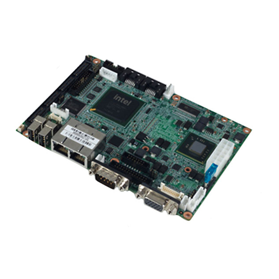
- Page 1 User Manual PCM-9362 3.5" Biscuit with Intel® Atom® N450/D510, VGA, LVDS, 2 Giga- LAN, USB, SATA, Mini PCIe and...
- Page 2 The documentation and the software included with this product are copyrighted 2009 by Advantech Co., Ltd. All rights are reserved. Advantech Co., Ltd. reserves the right to make improvements in the products described in this manual at any time without notice.
- Page 3 Because of Advantech’s high quality-control standards and rigorous testing, most of our customers never need to use our repair service. If an Advantech product is defec- tive, it will be repaired or replaced at no charge during the warranty period. For out- of-warranty repairs, you will be billed according to the cost of replacement materials, service time and freight.
-
Page 4: Packing List
Packing List Before installation, please ensure the following items have been shipped: Item Part Number 1 PCM-9362 SBC 1 Startup manual 1 Utility CD 1 mini jumper pack Cables Part Number Description 1700006291 SATA cable 30cm 1703060191 Keyboard/mouse cable 1*6P-2.0/M-DIN 6P(F)*2 19cm... -
Page 5: Table Of Contents
Super I/O Configuration .............. 25 Figure 3.6 Super I/O Configuration..........25 3.3.4 Hardware Health Configuration........... 26 Figure 3.7 Hardware health configuration........26 3.3.5 ACPI Settings................27 Figure 3.8 ACPI Settings ............27 Figure 3.9 General ACPI Configuration ........28 PCM-9362 User Manual... - Page 6 Table A.1: CN1: Audio ............... 62 Table A.2: CN2: SATA............... 62 Table A.3: CN3: SATA............... 63 Table A.4: CN4: GPIO ............... 63 Table A.5: CN5: HDD & PWR LED..........64 Table A.6: CN6: 12V AT Power Input ........64 PCM-9362 User Manual...
- Page 7 Table A.25:CN25: External USB..........79 Table A.26:CN26: COM1 ............79 Table A.27:CN27: VGA............... 80 Table A.28:CN28: Mini PCIE lock..........81 Table A.29:CN29: Mini PCIE slot..........82 Table A.30:CN30: DDR2 SODIMM..........84 Table A.31:CN31: BIOS Socket..........89 Table A.32:CN32: CF..............89 PCM-9362 User Manual...
- Page 8 PCM-9362 User Manual viii...
-
Page 9: Chapter 1 General Introduction
Chapter General Introduction This chapter gives background information on the PCM-9362. Sections include: Introduction Product feature Specifications... -
Page 10: Introduction
2GB, has six USB 2.0 compatible ports, two Giga-LAN (1000Mbps) interface, LVDS and VGA support, HD (High Definition) Audio, and one Mini-PCIe expansion. In addi- tion, PCM-9362 also supports two SATA, four COM ports and one CF slot. Product Feature General CPU: Intel®... -
Page 11: Specifications
6 USB 2.0 ports which are high-speed, full- speed, and low-speed USB Interface capable USB Connector:(USB1~4) 2 set 5 x 2-pin Hirose DF13 type Full ACPI (Advanced Configuration andPower Interface) 2.0 Power Management Supports S0, S1, S3,S4, S5 BIOS AMI 16Mb Flash BIOS via SPI PCM-9362 User Manual... -
Page 12: Mechanical Specification
24.4mm (Heatsink with FAN for D510 SKU) 20mm (Heatsink without FAN for N450 SKU) 1.3.2.3 Height on Bottom (mm) 7.90 mm (CF Socket) 1.3.2.4 Weight (g) with Heatsink 110g(Heatsink with FAN for D510 SKU) 88g(Heatsink without FAN for N450 SKU) PCM-9362 User Manual... -
Page 13: Electrical Specification
Operating Humidity:10% ~ 90% Relative Humidity, non-condensing 1.4.0.2 Operating Temperature Operating temperature: 0 ~ 60°C (32~140°F) 1.4.0.3 Storage Humidity Standard products (0 ~ 60°C) Relative Humidity: 95% @ 60°C 1.4.0.4 Storage Temperature Standard products (0 ~ 60°C) Storage temperature: -20~70°C PCM-9362 User Manual... - Page 14 PCM-9362 User Manual...
-
Page 15: Chapter 2 H/W Installation
Chapter H/W installation This chapter explains the setup procedures of the PCM-9362 hard- ware, including instructions on setting jumpers and connecting peripherals, switches, indicators and mechanical drawings. Be sure to read all safety precautions before you begin the installation procedure. -
Page 16: Jumpers
(1-2) RS232 (3-4) RS485 (5-6) RS422 Table 2.3: J3: AT / ATX Power SEL Part Number 1653002101 Footprint HD_2x1P_79_D Description PIN HEADER 2*1P 180D(M)SQUARE 2.0mm DIP W/O Pb Setting Function (1-2) AT Power SEL EMPTY ATX Power PCM-9362 User Manual... -
Page 17: Table 2.4: J4: Clear Coms
PIN HEADER 3*1P 180D(M) 2.0mm DIP SQUARE W/O Pb Setting Function (1-2) Normal (2-3) Clear CMOS Table 2.5: J5: PAN VOL SEL Part Number 1653003101 Footprint HD_3x1P_79_D Description PIN HEADER 3*1P 180D(M) 2.0mm DIP SQUARE W/O Pb Setting Function (1-2) (2-3) PCM-9362 User Manual... -
Page 18: Jumper Description
Generally, you simply need a standard cable to make most connections. Warning! To avoid damaging the computer, always turn off the power supply before setting jumpers. Clear CMOS. Before turning on the power sup- ply, set the jumper back to 3.0 V Battery On. PCM-9362 User Manual... -
Page 19: Connectors
CN20 Power Switch (Low Active ) CN21 CN22 Standby Power Input CN23 Reset CN24 External USB CN25 External USB CN26 COM1 CN27 CN28 Mini PCIE lock CN29 Mini PCIE slot CN30 DDR2 SODIMM CN31 BIOS Socket CN32 PCM-9362 User Manual... -
Page 20: Connector Settings
2.2.2.7 COM Port Connector (CN7, CN12,CN26) The PCM-9362 provides 4 serial ports (COM1, COM3 & COM4: RS-232; COM2: RS- 232/422/485) in one DB-9 connector (CN26) for COM1 and one 7*2P pin header (CN12) for COM2 and one 10*2P pin header(CN7) for COM3 & COM4. It provides connections for serial devices (a mouse, etc.) or a communication network. - Page 21 2.2.2.10 Inverter Power Connector (CN13) PCM-9362 can provide +5 V and +12 V and signal to LCD inverter board via CN13. 2.2.2.11 USB Connectors (CN14, CN15, CN24, CN25) The board provides up to six USB (Universal Serial Bus) ports.
- Page 22 2.2.2.15 LPT Connector (CN21) PCM-9362 can support LPT via CN21. LPT (Line Print Terminal) is the original, yet still common, name of the parallel port interface on IBM PC-compatible computers. It was designed to operate a text printer that used IBM's 8-bit extended ASCII charac- ter set.
-
Page 23: Mechanical
Mechanical 2.3.1 Jumper and Connector Location Figure 2.1 Jumper and Connector layout (Component side) Figure 2.2 Jumper and Connector layout (Solder side) PCM-9362 User Manual... -
Page 24: Board Dimension
2.3.2 Board Dimension Figure 2.3 Board Dimension layout (Component side) PCM-9362 User Manual... -
Page 25: Figure 2.4 Board Dimension Layout (Solder Side)
Figure 2.4 Board Dimension layout (Solder side) Figure 2.5 Board Dimension layout (Coastline) PCM-9362 User Manual... - Page 26 PCM-9362 User Manual...
-
Page 27: Chapter 3 Bios Settings
Chapter BIOS settings... -
Page 28: Figure 3.1 Setup Program Initial Screen
AMIBIOS has been integrated into many motherboards for over a decade. With the AMIBIOS Setup program, you can modify BIOS settings and control the various sys- tem features. This chapter describes the basic navigation of the PCM-9362 BIOS setup screens. -
Page 29: Main Setup
Date using the <Arrow> keys. Enter new values through the keyboard. Press the <Tab> key or the <Arrow> keys to move between fields. The date must be entered in MM/DD/YY format. The time must be entered in HH:MM:SS format. PCM-9362 User Manual... -
Page 30: Advanced Bios Features Setup
Advanced BIOS Features Setup Select the Advanced tab from the PCM-9362 setup screen to enter the Advanced BIOS Setup screen. You can select any of the items in the left frame of the screen, such as CPU Configuration, to go to the sub menu for that item. You can display an Advanced BIOS Setup option by highlighting it using the <Arrow>... -
Page 31: Cpu Configuration
CPU speed is controlled by the operating system. Intel® C-STATE tech This item allows the CPU to save more power under idle mode. Enhanced C-States CPU idle set to enhanced C-States, disabled by Intel® C-STATE tech item. PCM-9362 User Manual... -
Page 32: Ide Configuration
Hard Disk Write Protect Disable/Enable device write protection. This will be effective only if the device is accessed through BIOS. IDE Detect Time Out (Sec) This item allows you to select the time out value for detecting ATA/ATAPI device(s). PCM-9362 User Manual... -
Page 33: Super I/O Configuration
This item allows you to select serial port1 ~ port4 of IRQ. RS-485 Control for SP2 This item allows you to select RS485 control. Auto Direction Control Select This item allows you to enable or disable auto flow control function. PCM-9362 User Manual... -
Page 34: Hardware Health Configuration
3.3.4 Hardware Health Configuration Figure 3.7 Hardware health configuration H/W Health Function This item allows you to control H/W monitoring. Temperature & Voltage show CPU/System Temperature Vcore / +3.3Vin / +5Vin / +12Vin / VBAT PCM-9362 User Manual... -
Page 35: Acpi Settings
3.3.5 ACPI Settings Figure 3.8 ACPI Settings PCM-9362 User Manual... -
Page 36: Figure 3.9 General Acpi Configuration
3.3.5.1 General ACPI Configuration Figure 3.9 General ACPI Configuration Suspend mode Select the ACPI state used for system suspend. Report Video on S3 Resume This item allows you to invoke VA BIOS POST on S3/STR resume. PCM-9362 User Manual... -
Page 37: Figure 3.10Advanced Acpi Configuration
This item allows you to enable RSDP pointers to 64-bit fixed system description tables. ACPI APIC support Include APIC table pointer to RSDT pointer list. AMI OEMB table Include OEMB table pointer to R(x)SDT pointer lists. Headless mode Enable / Disable Headless operation mode through ACPI. PCM-9362 User Manual... -
Page 38: Figure 3.11Chipset Acpi Configuration
Allows you to configure Intel's Energy Lake power management technology. APIC ACPI SCI IRQ Enable/Disable APIC ACPI SCI IRQ. USB Device Wakeup From S3/S4 Enable/Disable USB Device Wakeup from S3/S4. High Performance Event Timer Enable/Disable High performance Event timer. PCM-9362 User Manual... -
Page 39: Ahci Configuration
3.3.6 AHCI Configuration Figure 3.12 AHCI Configuration AHCI Port0 / Port1 While entering setup, BIOS auto detects the presence of IDE devices. This displays the status of auto detection of IDE device. PCM-9362 User Manual... -
Page 40: Apm Configuration
Resume On Ring Enable / Disable RI to generate a wake event. Resume On PME# Enable / Disable PME to generate a wake event. Resume On RTC Alarm Enable / Disable RTC to generate a wake event. PCM-9362 User Manual... -
Page 41: Event Log Configuration
Figure 3.14 Event Log Configuration View Event Log View all unread events on the event Log. Mark all events as read Mark all unread events as read. Clear Event Log Discard all events in the event Log. PCM-9362 User Manual... -
Page 42: Mps Configuration
3.3.9 MPS Configuration Figure 3.15 MPS Configuration MPS Revision This item allows you to select MPS reversion. PCM-9362 User Manual... -
Page 43: Smbios Configuration
3.3.10 Smbios Configuration Figure 3.16 Smbios Configuration Smbios Smi Support SMBIOS SMI wrapper support for PnP function 50h-54h. PCM-9362 User Manual... -
Page 44: Usb Configuration
EHCI driver. Hotplug USB FDD Support A dummy FDD device is created that will be associated with the hotplugged FDD later. Auto option creates this dummy device only if there is no USB FDD present. PCM-9362 User Manual... -
Page 45: Figure 3.18Usb Mass Storage Device Configuration
If Auto, USB devices less than 530MB will be emulated as a floppy drive and the remaining as hard drive. Force FDD option can be used to force a FDD formatted drive to boot as FDD (Ex. ZIP drive). PCM-9362 User Manual... -
Page 46: Advanced Pci/Pnp Settings
Advanced PCI/PnP Settings Select the PCI/PnP tab from the PCM-9362 setup screen to enter the Plug and Play BIOS Setup screen. You can display a Plug and Play BIOS Setup option by highlight- ing it using the <Arrow> keys. All Plug and Play BIOS Setup options are described in this section. -
Page 47: Boot Settings
When set to Reserved will specify which DMA will be reserved for use by legacy ISA devices. Reserved Memory Size This item allows you to reserve the size of memory block for legacy ISA device. Boot Settings Figure 3.20 Boot Setup Utility PCM-9362 User Manual... -
Page 48: Boot Settings Configuration
Hit "DEL' Message Display Displays -Press DEL to run Setup in POST. Interrupt 19 Capture This item allows options for ROMs to trap interrupt 19. Bootsafe function This item allows you to enable or disable the bootsafe function. PCM-9362 User Manual... -
Page 49: Security Setup
Security Setup Figure 3.22 Password Configuration Select Security Setup from the PCM-9362 Setup main BIOS setup menu. All Security Setup options, such as password protection and virus protection are described in this section. To access the sub menu for the following items, select the item and press <Enter>:... -
Page 50: Advanced Chipset Settings
Advanced Chipset Settings Figure 3.23 Advanced Chipset Settings PCM-9362 User Manual... -
Page 51: North Bridge Chipset Configuration
This item allows you to free 15MB-16MB of memory size for some ISA devices. Initate Graphic Aadapter This item allows you to select which graphics controller to use as the primary boot device. Internal Graphics Mode Select Select the amount of system memory used by the Internal graphics device. PCM-9362 User Manual... -
Page 52: Figure 3.25Video Function Configuration
Boot Display Device Select boot display device at post stage. Flat Panel Type This item allows you to select which panel resolution you want. Spread Spectrum Clock This item allows you to enable or disable the spread spectrum clock. PCM-9362 User Manual... -
Page 53: South Bridge Chipset Configuration
Enables or disables GbE LAN wake up from S5 function. HDA Controller Enables or disables the HDA controller. SMBUS Controller Enables or disables the SMBUS controller. SLP_S4# Min. Assertion Width This item allows you to set a delay of sorts. PCM-9362 User Manual... -
Page 54: Exit Option
Select Exit Discarding Changes from the Exit menu and press <Enter>. The following message appears: Discard Changes and Exit Setup Now? [Ok] [Cancel] Select Ok to discard changes and exit. Discard Changes Select Discard Changes from the Exit menu and press <Enter>. PCM-9362 User Manual... -
Page 55: Load Optimal Defaults
3.8.3 Load Optimal Defaults The PCM-9362 automatically configures all setup items to optimal settings when you select this option. Optimal defaults are designed for maximum system performance, but may not work best for all computer applications. In particular, do not use the Opti- mal Defaults if your computer is experiencing system configuration problems. - Page 56 PCM-9362 User Manual...
-
Page 57: Chapter 4 S/W Introduction & Installation
Chapter S/W Introduction & Installation... -
Page 58: S/W Introduction
S/W Introduction The mission of Advantech Embedded Software Services is to "Enhance quality of life with Advantech platforms and Microsoft Windows embedded technology.” We enable Windows embedded software products on Advantech platforms to more effectively support the embedded computing community. Customers are freed from the hassle of dealing with multiple vendors (Hardware suppliers, System integrators, Embedded OS distributor) for projects. -
Page 59: Software Apis
The benefit of using SUSI is portability. The same set of API is defined for different Advantech hardware platforms. Also, the same set of API is implemented in different Operating Systems including Windows XP and Windows CE. -
Page 60: Susi Utilities
However, due to the inaccuracy among many commercially available hardware mon- itoring chips, Advantech has developed a unique scheme for hardware monitoring - achieved by using a dedicated micro-processor with algorithms specifically designed for providing accurate, real-time and reliable data content; helping protect your sys- tem in a more reliable manner. -
Page 61: Susi Installation
If a previous version is located, please see the section of [Maintenance Setup]. If it is not located, the following screen shot opens. Click Next. PCM-9362 User Manual... -
Page 62: Susi Sample Programs
Windows CE In windows CE, there are three ways to install the SUSI Library, you can install it manually or use Advantech CE-Builder to install the library or just copy the programs and the library onto a compact flash card. - Page 63 The GPIO pin assignments of the supported platforms are located in Appendix B. Test Read Single Input Pin – Click the radio button- Single-Pin. – Key in the pin number to read the value of the input pin. The Pin number starts from '0'. PCM-9362 User Manual...
- Page 64 Key in the slave device address in Slave address field. – Key in the register offset in Register Offset field. – Click the READ A BYTE button and then a byte of data from the device will be shown on the Result field. PCM-9362 User Manual...
- Page 65 Key in the slave device address in the Slave address field. – Key in the register offset in the Register Offset field. – Click the READ SMBus DATA button and then a word of data from the device will be shown on the Result field. PCM-9362 User Manual...
- Page 66 The application can turn on or turn off the screen shot freely, and it also can tune the brightness of the panels if your platform is being supported. You can test the function- alities of VGA control as follows: PCM-9362 User Manual...
- Page 67 Before the timer counts down to zero, you can reset the timer by clicking the REFRESH button. After you click this button, the Timeout Countdown field will display the value of the SET TIMEOUT field. If you want to stop the watchdog timer, you just click the STOP button. PCM-9362 User Manual...
- Page 68 If certain data values are not supported by the platform, the correspondent data field will be grayed-out with a value of 0. For More detail PCM-9362 software API user manual, please contact your dealer or Advantech AE. We also include these manuals in this CD.
-
Page 69: Appendix Apin Assignments
Appendix PIN Assignments... -
Page 70: Pin Assignments
BOX HEADER SMD 5*2 180D (M) 2.0mm Pin Name LOUTR LINR LOUTL LINL MIC1R MIC1L Matching Cable : 1703100152 Table A.2: CN2: SATA Part Number 1654002320 Footprint FOX_LD1107V-S33T5 Description Serial ATA 7P 1.27 90D(M) SMD LD1107V-S33T5 Pin Name PCM-9362 User Manual... -
Page 71: Table A.3: Cn3: Sata
FOX_LD1107V-S33T5 Description Serial ATA 7P 1.27 90D(M) SMD LD1107V-S33T5 Pin Name Table A.4: CN4: GPIO Part Number 1653005261 Footprint HD_5x2P_79 Description PIN HEADER SMD 5*2P 180D(M) 2.0mm Pin Name GPIO4 GPIO0 GPIO5 GPIO1 GPIO6 GPIO2 GPIO7 GPIO3 PCM-9362 User Manual... -
Page 72: Table A.5: Cn5: Hdd & Pwr Led
WAFER BOX 2.0mm 6P 180D(M) W/LOCK Pin Name Power LED+ Power LED- HDD LED+ HDD LED- Table A.6: CN6: 12V AT Power Input Part Number 1655404090 Footprint ATXCON-2X2-42 Description ATX PWR CONN. 2*2P 180D 4.2mm 24W4310-04S10-01T Pin Name +12V +12V PCM-9362 User Manual... -
Page 73: Table A.7: Cn7: Com3/Com4
Table A.7: CN7: COM3/COM4 Part Number 1653210260 Footprint HD_10x2P_79_BOX Description BOX HEADER 10*2P 180D(M) 2.0mm SMD W/O Pb Pin Name DCD3# DSR3# RXD3 RTS3# TXD3 CTS3# DTR3# RI3# DCD4# DSR4# RXD4 RTS4# TXD4 CTS4# DTR4# RI4# PCM-9362 User Manual... -
Page 74: Table A.8: Cn8: At/Atx Power Input
Table A.8: CN8: AT/ATX Power Input Part Number 1655412090 Footprint ATXCON-2X6V-42 Description Power CONN.6*2P 180D(M) DIP W/Fixed Lock Pin Name +5VSB PSON# +12V Matching Cable : 1700000265 PCM-9362 User Manual... -
Page 75: Table A.9: Cn9: Mio 2.0
B/B CONN. 80*2P 180D SMD 0.8mm QSE-080-01-F-D-A Pin Name USB_OC# USB_D- USB_D+ LPC_CLK48M GPIO1 GPIO2 LPC_SUSCLK LPC_DRQ#0 Reserved CBE#0 AD10 AD11 AD12 AD13 AD14 AD15 CBE#1 SERR# PERR# STOP# PME# INTA# INTB# REQ0 REQ1 REQ2 REQA GNTA CLK0 PCM-9362 User Manual... - Page 76 Table A.9: CN9: MIO 2.0 PCIE_RX3- PCIE_RX3+ PCIE_TX3- PCIE_TX3+ PCIE_CLK3- PCIE_CLK3+ PCIE_RX1- PCIE_RX1+ PCIE_TX1- PCIE_TX1+ PCIE_CLK1- PCIE_CLK1+ PCIE_RST Reserved Reserved Reserved SDVO_CLK- SDVO_CLK+ SDVO_BLUE- SDVO_BLUE+ SDVO_GREEN- SDVO_GREEN+ SDVO_RED- SDVO_RED+ Reserved SMB_CLK SMB_DAT Global Reset PWROK_5V GPIO3 LPC_FRAME# LPC_AD0 LPC_AD1 LPC_AD2 PCM-9362 User Manual...
- Page 77 CBE#2 AD16 AD17 AD18 AD19 AD20 AD21 AD22 AD23 CBE#3 AD24 AD25 AD26 AD27 AD28 AD29 AD30 AD31 INTC# INTD# GNT0 GNT1 GNT2 PCIRST Ring Serial IRQ PCIE_RX4- PCIE_RX4+ PCIE_TX4- PCIE_TX4+ PCIE_CLK4- PCIE_CLK4+ PCIE_RX2- PCIE_RX2+ PCIE_TX2- PCIE_TX2+ PCM-9362 User Manual...
- Page 78 Table A.9: CN9: MIO 2.0 PCIE_CLK2- PCIE_CLK2+ PCIE_WAKE# ACPI_S3 ACPI_S5 Reserved SDVO_CLDAT SDVO_CLCLK SDVO_FLDSTALL+ SDVO_FLDSTALL- SDVO_TVCLKIN- SDVO_TVCLKIN+ SDVO_INT- SDVO_INT+ Reserved +12V +5VSB PCM-9362 User Manual...
-
Page 79: Table A.10:Cn10: Ps2
WAFER BOX 2.0mm 6P 180D(M) W/LOCK Pin Name KBCLK KBDAT MSCLK MSDAT Matching Cable: 1703060053 1700060202 Table A.11: CN11: SMBus Part Number 1655904020 Footprint FPC4V-125M Description Wafer SMT 1.25mmS/T type 4P 180D(M) 85205-04001 Pin Name SMB_DAT SMB_CLK PCM-9362 User Manual... -
Page 80: Table A.12:Cn17: Com2
DSR# RTS# CTS# DTR# 422/485TX+ 422/485TX- 422RX+ 422RX- Matching Cable : 1701140201 Table A.13: CN13: Inverter Power Output Part Number 1655000453 Footprint WHL5V-2M-24W1140 Description WAFER BOX 2.0mm 5P 180D(M) DIP WO/pb JIH VEI Pin Name +12V ENABKL PCM-9362 User Manual... -
Page 81: Table A.14:Cn14: Internal Usb
Pin Name A_D- B_D- A_D+ B_D+ Matching Cable : 1703100121 Table A.15: CN15: Internal USB Part Number 1653005260 Footprint HD_5x2P_79_N10 Description PIN HEADER 2*5P 180D(M) 2.0mm SMD IDIOT-PROOF Pin Name A_D- B_D- A_D+ B_D+ Matching Cable : 1703100121 PCM-9362 User Manual... -
Page 82: Table A.16:Cn16: 18 Bits Lvds Panel
Table A.16: CN16: 18 bits LVDS Panel Part Number 1653910261 Footprint SPH10X2 Description *CONN. SMD 10*2P 180D(M)DF13-20DP-1.25V(91) HRS Pin Name LVDS0_D0+ LVDS0_D0- LVDS0_D1+ LVDS0_D1- LVDS0_D2+ LVDS0_D2- LVDS0_CLK+ LVDS0_CLK- +5V or +3.3V +5V or +3.3V PCM-9362 User Manual... -
Page 83: Table A.17:Cn17: Lan
PHONE JACK RJ45 28P DIP Gold flash RTB-19GB9J1A Pin Name TX+(10/100),BI_DA+(GHz) TX-(10/100),BI_DA-(GHz) RX+(10/100),BI_DB+(GHz) BI_DC+(GHz) BI_DC-(GHz) RX-(10/100),BI_DB-(GHz) BI_DD+(GHz) BI_DD-(GHz) Table A.18: CN18: LAN1 Part Number 1652002996 Footprint RJ45_14P_RTA-195AAK1A Description Phone Jack RJ45 14P 90D(M) DIP RTA-195AAK1A Pin Name PCM-9362 User Manual... -
Page 84: Table A.19:Cn19: Lan2
1655302020 Footprint WF_2P_79_BOX_R1_D Description WAFER BOX 2P 180D(M) 2.0mm W/Lock Pin Name PSIN Table A.21: CN11: LPT Part Number 1653213260 Footprint HD_13x2P_79_BOX Description BOX HEADER 13*2P 180D(M) 2.0mm SMD Pin Name STROBE# AUTOFEED# ERROR# INIT# SLCT IN# PCM-9362 User Manual... -
Page 85: Table A.22:Cn22: Standby Power Input
Table A.21: CN11: LPT ACK# BUSY SLCT Matching Cable : 1700260250 1700001531 Table A.22: CN22: Standby Power Input Part Number 1655303020 Footprint WHL3V-2M Description WAFER BOX 2.0mm 3P 180D w/LOCK Pin Name +5VSB PSON# PCM-9362 User Manual... -
Page 86: Table A.23:Cn2: Reset
Table A.23: CN2: Reset Part Number 1655302020 Footprint WF_2P_79_BOX_R1_D Description WAFER BOX 2P 180D(M) 2.0mm W/Lock Pin Name RESET# Table A.24: CN24: External USB Part Number 1654904105 Footprint USB-V-4A Description USB CON. 4P 90D(F) DIP A TYPE RoHS Pin Name PCM-9362 User Manual... -
Page 87: Table A.25:Cn25: External Usb
1654904105 Footprint USB-V-4A Description USB CON. 4P 90D(F) DIP A TYPE RoHS Pin Name Table A.26: CN26: COM1 Part Number 1654000056 Footprint DBCOM-VM5MS Description D-SUB CON. 9P 90D(M)DIP 070241MR009S200ZU SUYIN Pin Name DCD# DTR# DSR# RTS# CTS# PCM-9362 User Manual... -
Page 88: Table A.27:Cn27: Vga
Table A.27: CN27: VGA Part Number 1654000055 Footprint DBVGA-VF5MS Description D-SUB Conn. 15P 90D(F) DIP 070242FR015S200ZU Pin Name GREEN BLUE DDAT HSYNC VSYNC DCLK PCM-9362 User Manual... -
Page 89: Table A.28:Cn28: Mini Pcie Lock
Table A.28: CN28: Mini PCIE lock Part Number 1654002539 Footprint FOX_AS0B226-S68K7F_HOLDER Description MINI PCI Express LATCH 52P 90D SMD 6.8mm Pin Name PCM-9362 User Manual... -
Page 90: Table A.29:Cn29: Mini Pcie Slot
MINI PCI express 52P 90D SMD H=6.8mm Pin Name WAKE# +3.3V or +3.3VSB +1.5V CLKREQ# REFCLK- REFCLK+ PERST# PERn0 +3.3VSB PERp0 +1.5V SMB CLK PETn0 SMB DAT PETp0 USB D- USB D+ +3.3V or +3.3VSB +3.3V or +3.3VSB PCM-9362 User Manual... - Page 91 Table A.29: CN29: Mini PCIE slot +1.5V +3.3V or +3.3VSB PCM-9362 User Manual...
-
Page 92: Table A.30:Cn30: Ddr2 Sodimm
Part Number 1651000087 Footprint DDR-SODIMM-STD65 Description SKT DIMM 200P DDR2 H=6.5mm STD SMD WO/Pb Pin Name VREF DQ59 DQ63 DQ58 DQ62 DQS#7 DQS7 DQ57 DQ56 DQ61 DQ60 DQ51 DQ50 DQ55 DQ54 DQS#6 DQS6 CK1# DQ53 DQ49 DQ52 DQ48 PCM-9362 User Manual... - Page 93 Table A.30: CN30: DDR2 SODIMM DQ47 DQ43 DQ46 DQ42 DQS#5 DQS5 DQ45 DQ41 DQ44 DQ40 DQ39 DQ35 DQ38 DQ34 DQS#4 DQS4 DQ37 DQ33 DQ36 DQ32 CKE0 CKE1 +1.8V +1.8V +1.8V +1.8V PCM-9362 User Manual...
- Page 94 Table A.30: CN30: DDR2 SODIMM +1.8V +1.8V +1.8V +1.8V RAS# SCS#0 +1.8V +1.8V CAS# ODT0 SCS#1 +1.8V +1.8V ODT1 DQ31 DQ27 DQ30 DQ26 DQS#3 DQS3 DQ25 DQ29 DQ24 PCM-9362 User Manual...
- Page 95 Table A.30: CN30: DDR2 SODIMM DQ28 DQ19 DQ23 DQ18 DQ22 DQS#2 DQS2 DQ21 DQ17 DQ20 DQ16 DQ15 DQ11 DQ14 DQ10 CK0# DQS#1 DQS1 DQ13 DQ12 PCM-9362 User Manual...
- Page 96 Table A.30: CN30: DDR2 SODIMM DQS#0 DQS0 +3.3V PCM-9362 User Manual...
-
Page 97: Table A.31:Cn31: Bios Socket
Part Number 1651000682 Footprint SOCKET_8P_ACA-SPI-004-K01 Description IC SKT 8P SMD WO/Pb C ACA-SPI-004-K01 Pin Name HOLD# +3.3V Table A.32: CN32: CF Part Number 1653002919 Footprint CF_50P_CFCMD-35T15W100 Description CF Type2 Conn.50P 90D(M) SMD WO/Pb CFCMD-35T15W1 Pin Name CS0# PCM-9362 User Manual... - Page 98 Table A.32: CN32: CF CD2# CD1# PCM-9362 User Manual...
- Page 99 PCM-9362 User Manual...
- Page 100 No part of this publication may be reproduced in any form or by any means, electronic, photocopying, recording or otherwise, without prior written permis- sion of the publisher. All brand and product names are trademarks or registered trademarks of their respective companies. © Advantech Co., Ltd. 2009...
Need help?
Do you have a question about the PCM-9362 Series and is the answer not in the manual?
Questions and answers