Table of Contents
Advertisement
Quick Links
Advertisement
Table of Contents

Subscribe to Our Youtube Channel
Related Manuals for Advantech PCM-9377


Summary of Contents for Advantech PCM-9377
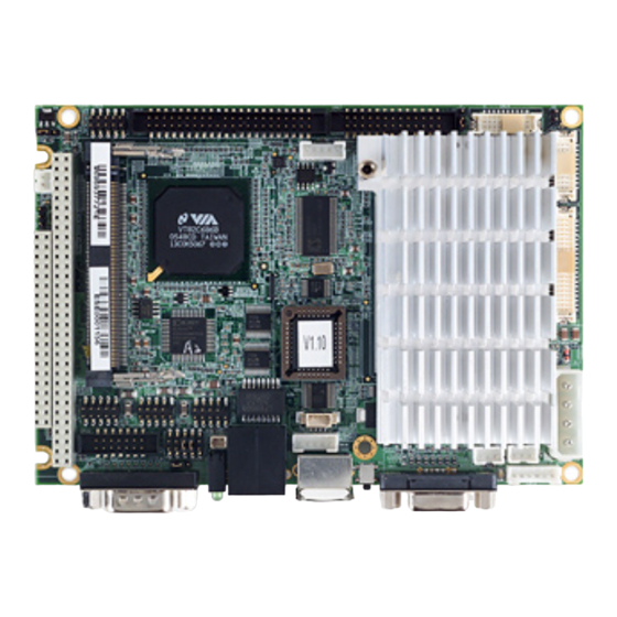
- Page 1 PCM-9377 3.5" SBC with VIA Mark, VGA/ LCD/LVDS/LAN/USB User Manual...
- Page 2 SMI is a trademark of Silicon Motion, Inc. Creative is a trademark of Creative Technology LTD. All other product names or trademarks are properties of their respective owners. For more information on this and other Advantech products, please visit our websites at: http://www.advantech.com http://www.advantech.com/eplatform For technical support and service, please visit our support website at: http://www.advantech.com/support...
- Page 3 Packing List Before you begin installing your card, please make sure that the following materials have been shipped: • 1 PCM-9377 SBC • 1 Startup manual • 1 Utility CD • 1 mini jumper pack p/n: 9689000002 • 1 Audio cable p/n: 1703100152 •...
- Page 4 Additional Information and Assistance 1.Visit the Advantech web site at www.advantech.com where you can find the latest information about the product. 2.Contact your distributor, sales representative, or Advantech's customer service center for technical support if you need additional assistance. Please have the following information ready before you call: •Product name and serial number...
- Page 5 This device complies with the requirements in part 15 of the FCC rules: Operation is subject to the fol- lowing two conditions: 1.This device may not cause harmful interference, 2.This device must accept any interference received, including interference that may cause undesired operation This equipment has been tested and found to com- ply with the limits for a Class A digital device, pursu-...
- Page 6 PCM-9377 User Manual...
-
Page 7: Table Of Contents
Contents Chapter 1 Introduction ............2 Introduction ............... 2 Features ................2 Specifications ..............2 1.3.1 Standard 3.5" Biscuit SBC Functions......2 1.3.2 VGA/LVDS Interface ............. 3 1.3.3 Ethernet Interface............3 1.3.4 Audio Function ............... 3 1.3.5 OS support ..............3 1.3.6 Mechanical and Environmental ........ - Page 8 Entering Setup ..............26 Figure 3.1:Award BIOS Setup initial screen ....27 Standard CMOS Setup ............ 27 Advanced BIOS Features ..........27 Figure 3.2:Advanced BIOS features screen....28 3.4.1 Virus Warning............... 28 3.4.2 CPU Internal Cache ............28 PCM-9377 User Manual viii...
- Page 9 3.4.3 External Cache.............. 28 3.4.4 CPU L2 cache ECC checking........28 3.4.5 Quick Power on Self Test ..........28 3.4.6 First/Second/Third/Other Boot Device......29 3.4.7 Swap Floppy Drive ............29 3.4.8 Boot up Floppy Seek............. 29 3.4.9 Boot Up NumLock Status..........29 3.4.10 Gate A20 Option............
- Page 10 Load fail-safe Defaults ............ 41 3.11 Load Optimized Defaults ..........41 3.12 Password Setting ............. 42 3.13 Save & Exit Setup ............42 3.14 Exit Without Saving ............43 Chapter 4 PCI SVGA/LCD Setup ........46 Introduction ..............46 PCM-9377 User Manual...
- Page 11 Display type and Dual Simultaneous Display ..... 46 4.1.2 CMOS setting for panel type ........46 Connections to Two Standard LCDs....... 47 4.2.1 TX26D01VM1CAA and PCM-9377......48 Table 4.1:Connections to TX26D01VM1CAA / PCM- 937748 Installation of the SVGA Driver ........49 4.3.1 Installation chipset ............
- Page 12 Table B.1:System I/O ports ........108 1st MB memory map............. 109 Table B.2:1st MB memory map ......... 109 DMA channel assignments..........109 Table B.3:DMA channel assignments ......109 Interrupt assignments ............ 110 Table B.4:Interrupt assignments ......... 110 PCM-9377 User Manual...
- Page 13 Appendix C Mechanical Drawings........112 Mechanical Drawings............ 112 Figure C.1:PCM-9377 Mechanical Drawing (Component Side)112 Figure C.2:PCM-9377 Mechanical Drawing (Solder Side)113 xiii...
- Page 14 PCM-9377 User Manual...
- Page 15 General Information This chapter gives background infor- mation on the PCM-9377. Sections include: • Introduction • Features • Specifications • Board layout and dimensions...
-
Page 16: Chapter 1 Introduction
LVDS interface or TV-out solution. For those who want superior performance for various low-power embed- ded application and PC/104 expansion slot, PCM-9377 uses an VIA Mark CPU processor clocked at 533 MHz and 800 MHz, in conjunction with graphic controller and DRAM memory through one SODIMM socket. -
Page 17: Vga/Lvds Interface
• Watchdog timer: 1~62 sec, 62-level time intervals system reset or IRQ11 • Expansion Interface: PC/104 and miniPCI type III • Battery: Lithium 3V/196 mAH • Power management: ACPI supported • Enhanced IDE interface: One channels supports up to two EIDE devices. BIOS auto-detect, PIO Mode 3 or Mode 4, supports UDMA 33/66 mode •... -
Page 18: Mechanical And Environmental
• For further information about OS support for this board, visit the fol- lowing web resource Advantech: website: www.advantech.com or please contact technical support center 1.3.6 Mechanical and Environmental • Dimensions: 145 x 102 mm (5.9"x 4.2") Mechanical Drawing (dxf file) is available. -
Page 19: Board Layout: Dimensions
1.4 Board layout: dimensions Figure 1.1: Board layout: Dimensions (Component Side) Figure 1.2: Board layout: Dimensions (Solder Side) Chapter 1... - Page 20 PCM-9377 User Manual...
- Page 21 Installation This chapter explains the setup proce- dures of the PCM-9377 hardware, including instructions on setting jump- ers and connecting peripherals, switches and indicators. Be sure to read all safety precautions before you begin the installation procedure.
-
Page 22: Chapter 2 Installation
Chapter 2 Installation 2.1 Jumpers The PCM-9377 has a number of jumpers that allow you to configure your system to suit your application. The table below lists the functions of the various jumpers. Table 2.1: Jumpers Label Function Clear CMOS... -
Page 23: Com2 & Wdg Select (J4)
+5 V *: default 2.2 Connectors On-board connectors link the PCM-9377 to external devices such as hard disk drives, a keyboard, or floppy drives. The table below lists the func- tion of each of the board’s connectors. Table 2.7: Connectors... - Page 24 LVDS Connector CN15 LCD Connector2 CN16 Inverter Power CN17 CN18 IrDA (SIP) CN20 Keyboard/ Mouse CN21 COM1 CN22 COM2 CN23 Print Port CN24 LAN1 CN25 miniPCI type III CN26 Audio CN27 GPIO CN28 SMBus CN29 USB1/2 CN30 USB3/4 PCM-9377 User Manual...
-
Page 25: Locating Connectors
2.3 Locating Connectors CN26 CN23 CN14 CN10 1 2 3 CN16 1 2 3 CN15 A2 B2 CN25 CN13 CN28 CN22 CN18 CN20 1 2 3 CN17 CN12 Figure 2.1: Connectors (component side) 1 2 3 1 2 3 Figure 2.2: Connectors (solder side) Chapter 2... - Page 26 Location Dimension Location Dimension A2 B2 CN10 1 2 3 PCM-9377 User Manual...
- Page 27 CN11 CN12 12 3 CN13 CN14 CN15 CN16 1 2 3 CN17 CN18 CN20 CN21 CN22 CN23 CN24 CN25 Chapter 2...
-
Page 28: Setting Jumpers
To “open” a jumper, you remove the clip. Sometimes a jumper will have three pins, labeled 1, 2 and 3. In this case you would connect either pins 1 and 2, or 2 and 3. PCM-9377 User Manual... - Page 29 open closed closed 2-3 The jumper settings are schematically depicted in this manual as follows:. open closed closed 2-3 A pair of needle-nose pliers may be helpful when working with jumpers. If you have any doubts about the best hardware configuration for your application, contact your local distributor or sales representative before you make any changes.
-
Page 30: Installing So-Dimm
Enhanced Integrated Device Electronics hard disk drives or CDROM to the board’s internal controller. Its IDE controller uses a PCI interface. This advanced IDE controller supports faster data transfer, PIO mode 3, mode 4 and up to UDMA33. PCM-9377 User Manual... -
Page 31: Connecting The Hard Drive
2.6.1 Connecting the hard drive Connecting drives is done in a daisy-chain fashion. This package includes One 44PIN IDE cable that can connect to 1.8" and 2.5" drives. Connect one end of the cable to Hard Drive connector. Make sure that the red (or blue) wire corresponds to pin 1 on the connector, which is labeled on the board (on the right side). -
Page 32: Power & Hdd Led Connector
Supplies main power to the board (+5 V), and to devices that require +12 2.11.3 ATX Feature connector (CN1) The PCM-9377 can support ATX power supply by CN1 connector. Note.: Be sure that the ATX power supply can take at least a 10 mA load on the 5 V standby lead (5VSB). -
Page 33: Audio Power Source Setting (J5)
2.12.2 Audio power source setting (J5) The board is designed to work with a single +5 volts power supply as audio interfaces usually function under +5 volts. However, most audio controllers require an independent +12 volts power source since this avoids noise interference from other digital circuits. -
Page 34: Crt Display Connector (Cn17)
2.14.3 Extension flat panel connector (CN15) CN15 consists of a 20-pin Hirose’s connector no. DF13A-20DP-1.25V. The PCM-9377 supports a 36-bit LCD panel which must be connected to both the CN13 (40-pin) and the CN15 (20-pin). The pin assignments for both CN13 and the CN15 can be found in Appendix C. -
Page 35: Watchdog Timer Action (J4)
The board provides optional TV-out module PCM-232 via CN13, CN15 and J3 jumper. To enable TV-out function, please connect PCM-232 module to PCM-9377 board and setup J3 jumper as bellow table. This module output supports composite video and S-video connectors. TC-out... -
Page 36: Floppy Drive Connector (Optional) (Cn11)
Appendix A. 2.21 IR connector (CN18) The board provides an IrDA port for transfer rates of 115 kbps. This con- nector supports the optional wireless infrared transmitting and receiving PCM-9377 User Manual... -
Page 37: Lcd Power Setting (J2)
SMBus is the System Management Bus and usually used it for low-speed system management communications. This Board supports SMBus for Advantech embedded API - SUSI (Secured and Unified Smart Interface). It allows a developer to interface a Windows XP or CE PC to a down- stream embedded system environment and transfer serial messages using the SMBus protocols. - Page 38 PCM-9377 User Manual...
- Page 39 Award BIOS Setup Chapter 3...
-
Page 40: Chapter 3 Award Bios Setup
If there is no number assigned to the patch code, please contact Advan- tech’s applications engineer to obtain an up-to-date patch code file. This will ensure that your CPU’s system status is valid. After ensuring that you PCM-9377 User Manual... -
Page 41: Standard Cmos Setup
have a number assigned to the patch code, press <Del> to allow you to enter the setup. Figure 3.1: Award BIOS Setup initial screen 3.3 Standard CMOS Setup Choose the “Standard CMOS Features” option from the “Initial Setup Screen” menu, and the screen below will be displayed. This menu allows users to configure system components such as date, time, hard disk drive, Video, Halt On, display, and memory. -
Page 42: Virus Warning
The commands are “Enabled” or “Disabled.” 3.4.5 Quick Power on Self Test Allows the system to skip certain tests while booting. This will decrease the time needed to boot the system. The commands are “Enabled” or “Disabled.” PCM-9377 User Manual... - Page 43 3.4.6 First/Second/Third/Other Boot Device Select your boot device priority. Choices are: Floppy, LS120, HDD-0, SCSI, CDROM, HDD-1, HDD-2, HDD-3, AIP100, LAN and disabled. 3.4.7 Swap Floppy Drive If the system has two floppy drives, choose enable to assign physical drive B to logical drive A and vice-versa. The commands are “enable” or “disable”.
- Page 44 To disable security, select “PASSWORD SET- TING” in the main menu. At this point, you will be asked to enter a password. Simply press <Enter> to disable security. When security is disabled, the system will boot, and you can enter Setup freely. PCM-9377 User Manual...
- Page 45 3.5 Advanced Chipset Feature Figure 3.3: Advanced Chipset Features screen 3.5.1 DRAM Timing by SPD 3.5.2 Memory Hole 3.5.3 P2C/C2P Concurrency 3.5.4 System BIOS Cacheable 3.5.5 Video RAM Cacheable Chapter 3...
- Page 46 3.5.16 OnChip modem The command is “Auto” or “Disable”. 3.5.17 CPU PCI Writer Buffer 3.5.18 PCI dynamic Bursting 3.5.19 PCI Master 0 WS Write 3.5.20 PCI Delay Transaction 3.5.21 PCI#2 Access#1 Retry 3.5.22 AGP Master 1 WS Write PCM-9377 User Manual...
- Page 47 3.5.23 AGP Master 1 WS Read The command for above items is “Enable” or “Disable”. 3.6 Integrated Peripherals Figure 3.4: Integrated Peripherals screen Chapter 3...
-
Page 48: Init Display First
This field allows you to set the operation mode of the parallel port. The setting “Normal” allows normal speed operation, but in one direction only. “EPP” allows bidirectional parallel port operation at maximum speed. “ECP” allows the parallel port to operate in bi-directional mode PCM-9377 User Manual... -
Page 49: Onboard Legacy Audio
and at a speed faster than the maximum data transfer rate. “ECP + EPP” allows normal speed operation in a two-way mode. 3.6.10 Onboard Legacy Audio Select Disable if you do not want to use AC-97 audio. The option is Dis- abled or Enabled. -
Page 50: Power Management Setup
3.7 Power Management Setup The power management setup controls the CPU card’s “green” features to save power. The following screen shows the manufacturer’s defaults: Figure 3.5: Power management setup screen 3.7.1 ACPI function The choice: Enabled, Disabled. PCM-9377 User Manual... -
Page 51: Power Management
3.7.2 Power Management This category allows you to select the type (or degree) of power saving and is directly related to the following modes: 1. Power Management 2. HDD Power Down 3. Doze Mode 4. Suspend Mode 3.7.2.1 Power Management There are four selections for Power Management, three of which have fixed mode settings Min. -
Page 52: Video Off Method
Resume Time. Date (of Month): Resume Time (hh: mm: ss). When Enabled, your can set the date and time at which the RTC (real- time clock) alarm awakens the system from Suspend mode. The choices: Enabled, Disabled. 3.7.9.7 Primary INTR-OFF, ON PCM-9377 User Manual... - Page 53 3.7.9.8 IRQs Activity Monitoring Figure 3.6: IRQs Activity Monitoring screen IRQ3 (COM 2) - Enabled, Disabled IRQ4 (COM 1) - Enabled, Disabled IRQ5 (LPT 2) - Enabled, Disabled IRQ6 (Floppy Disk) - Enabled, Disabled IRQ7 (LPT 1) - Enabled, Disabled IRQ8 (RTC Alarm) - Enabled, Disabled IRQ9 (IRQ2 Redir) - Enabled, Disabled IRQ10 (Reserved) - Enabled, Disabled...
-
Page 54: Pnp/Pci Configurations
Plug and Play devices but you must be using Windows 95 or above. 3.8.4 PCI/VGA Palette Snoop This is left at “Disabled.” 3.8.5 Assign IRQ for VGA 3.8.6 Assign IRQ for USB PCM-9377 User Manual... -
Page 55: Pc Health Status
3.9 PC Health Status Figure 3.8: PC Health Status screen You can see your system status from this section. Includes: Current CPU Temp. Current System Temp. Current CPUFAN1 Speed Current CPUFAN2 Speed VCore 2.5V 3.3V 3.10 Load fail-safe Defaults Yes/No 3.11 Load Optimized Defaults Yes/No Chapter 3... -
Page 56: Password Setting
CMOS memory of the chipset. The micropro- cessor will check this every time you turn your system on and compare this to what it finds as it checks the system. This record is required for the system to operate. PCM-9377 User Manual... -
Page 57: Exit Without Saving
3.14 Exit Without Saving Selecting this option and pressing <Enter> lets you exit the setup program without recording any new values or changing old ones. Chapter 3... - Page 58 PCM-9377 User Manual...
- Page 59 PCI SVGA/LCD Setup This chapter details the software con- figuration information. It shows you how to configure the card to match your application requirements. The AWARD System BIOS is covered in Chapter 4. Sections include: • Installation of SVGA drivers -for Window XP •...
-
Page 60: Chapter 4 Pci Svga/Lcd Setup
"CRT+LCD","CRT+TV", and "CRT+LVDS". This system is initially set to dual display mode. If you want to enable other display model, please set them up from the BIOS screen, or contact Advantech technical sup- port center. 4.1.2 CMOS setting for panel type The board system BIOS and custom drivers are located in a 512 Kbyte, Flash ROM device. -
Page 61: Connections To Two Standard Lcds
18-bit LCD 24-bit LCD (CN13, CN15) (CN13) 24-bit LVDS (CN14) 4.2 Connections to Two Standard LCDs Connector Table of 12.1" TTL Sharp LQ121S1DG31 800 x 600 5/3.3V (18 Bit) for PCM-9377 AMD Geode LX. Chapter 4... -
Page 62: Tx26D01Vm1Caa And Pcm-9377
TX26D01VM1CAA and PCM-9377 4.2.1 Table 4.1: Connections to TX26D01VM1CAA / PCM-9377 TX26D01VM1CAA PCM-9377 FH12-32S-0.5SH DF13A-40DP-1.25V Function Function DCLK SHFCLC DTMG M/DE VDD (3.3) 3.3V VDD (3.3) 3.3V TEST PCM-9377 User Manual... -
Page 63: Installation Of The Svga Driver
Table 4.1: Connections to TX26D01VM1CAA / PCM-9377 4.3 Installation of the SVGA Driver Complete the following steps to install the SVGA driver. Follow the pro- cedures in the flow chart that apply to the operating system that you are using within your board. - Page 64 1. Open “my computer”, right click on properties 2. Right click “Hardware/Device Manager” and add new device. PCM-9377 User Manual...
- Page 65 3. Find the chipset driver on driver CD and double click it to start installa- tion process. 4.Click on welcome, then click next. Chapter 4...
- Page 66 5.Click on next. 6.Click on finish. PCM-9377 User Manual...
-
Page 67: Installation Of Vga Driver
4.3.2 Installation of VGA driver 1. Install driver CD, find VGA folder and enter it. 2. Double click setup and start to run installation process. 3. Select “YES” to restart your computer after installation is finished. Chapter 4... -
Page 68: Dual Simultaneous Display
4.3.3 Dual Simultaneous Display To set up dual display under 2000/XP follow these steps: 1. Select “Control panel”, “Display” “Setting” 2. Click “Advanced”, “S3 display setting”. PCM-9377 User Manual... -
Page 69: Further Information
4.4 Further Information For further information about the AGP/VGA installation in your PCM- 9377, including driver updates, troubleshooting guides and FAQ lists, visit the following web resources: Intel website: www.intel.com Advantech websites: www.advantech.com www.advantech.com.tw Chapter 4... - Page 70 PCM-9377 User Manual...
- Page 71 Audio Setup The board is equipped with an audio interface that records and plays back CD-quality audio. This chapter pro- vides instructions for installing the soft- ware drivers included on the audio driver diskettes.
-
Page 72: Chapter 5 Audio Setup
Note: The files on the software installation diskette are compressed. Do not attempt to install the drivers by copying the files manually. You must use the supplied SETUP program to install the drivers. 5.2.2 Windows XP drivers PCM-9377 User Manual... - Page 73 Open device manage, right click on audio and click on properity. Chapter 5...
- Page 74 Find the Audio folder in the driver CD and start to run the “setup” program. PCM-9377 User Manual...
- Page 75 Please click “YES” to restart the computer after installation is fin- ished. Chapter 5...
- Page 76 PCM-9377 User Manual...
- Page 77 Ethernet Interface This chapter provides information on Ethernet configuration. Sections include: • Introduction • Installation of Ethernet drivers for Windows XP • Further information...
-
Page 78: Chapter 6 Ethernet Interface
You will quickly and successfully complete the installation, even if you are not familiar with instructions for MS-DOS or Windows. Note: The windows illustrations in this chapter are examples only. Follow the steps and pay atten- tion to the instructions which appear on your screen. PCM-9377 User Manual... -
Page 79: Install Realtek Rtl8100 Chipset
6.2.1 Install Realtek RTL8100 chipset It is auto-detec RTL8100 LAN chipset under Win XP OS without any driver installation. Hereby, we would like to introduce the installation step when user run Win 2000 OS at their computing system. Find “ RTL8100” folder at driver CD, click “setup” for installation Chapter 6... - Page 80 Click “Finish” when the installation program is completed and restart the computing system. PCM-9377 User Manual...
-
Page 81: Installation For Windows Xp
6.2.2 Installation for Windows XP a. Select "Start", "Settings". "Control Panel". b. Double click "Network". Chapter 6... - Page 82 Click “Add new hardware wizard” and prepare to install network function PCM-9377 User Manual...
- Page 83 Choose Hardware Device “Ethernet Controller” Chapter 6...
- Page 84 Insert the CD into D: drive a. Fill in the Find the LAN chipset folder at the driver CD. b. Click “OK”. PCM-9377 User Manual...
- Page 85 Choose the "Intel(R) GD82559ER PCI Adapter" item Click “Next” Chapter 6...
-
Page 86: Further Information
Make sure the configurations of relative items are set correctly b. Click “OK” 6.3 Further information Intel website: www.intel.com Advantech websites:www.advantech.com www.advantech.com.tw PCM-9377 User Manual... - Page 87 Pin Assignments This appendix contains information of a detailed or specialized nature. It includes: • Stand-by Power Input • Power Input • SODIMM (H:5.6mm) • Power Switch • CPU_FAN • External Battery • ISA -5V & -12V Input • CF (Compact Flash ) •...
-
Page 88: Appendix A Pin Assignments
Wafer Box 2.0mm 3P180D w/Lock Pin Name Signal Type +5 V A.2 Power Input (CN2) Table A.2: Power Input (CN2) Part Number 1655204030 Description Housing 5.08mm 4P 180D Male w/o Lock Pin Name Signal Type +12 V +5 V PCM-9377 User Manual... -
Page 89: Sodimm (Cn3)
A.3 SODIMM (CN3) Table A.3: SODIMM (CN3) Part Number 1651500002 Description *S.O.DIMM SKT 0.8mm 144P (N=30, M=42) H=5.6180D Pin Name Signal Type MD32 MD33 MD34 MD35 +3.3 V +3.3 V MD36 MD37 MD38 MD39 DQM0 DQM4 DQM1 DQM5 +3.3V Appendix A... - Page 90 Table A.3: SODIMM (CN3) Part Number 1651500002 Description *S.O.DIMM SKT 0.8mm 144P (N=30, M=42) H=5.6180D Pin Name Signal Type +3.3V MD40 MD41 MD10 MD42 MD11 MD43 +3.3V +3.3V MD12 MD44 MD13 MD45 MD14 MD46 MD15 MD47 PCM-9377 User Manual...
- Page 91 Table A.3: SODIMM (CN3) Part Number 1651500002 Description *S.O.DIMM SKT 0.8mm 144P (N=30, M=42) H=5.6180D Pin Name Signal Type M_CLK0 M_CKE0 +3.3V +3.3V M_RAS M_CAS M_WE M_CKE1 M_CS0 MA14 M_CS1 M_OE M_CLK1 +3.3V +3.3V MD16 Appendix A...
- Page 92 Table A.3: SODIMM (CN3) Part Number 1651500002 Description *S.O.DIMM SKT 0.8mm 144P (N=30, M=42) H=5.6180D Pin Name Signal Type MD48 MD17 MD49 MD18 MD50 MD19 MD51 MD20 MD52 MD21 MD53 MD22 MD54 MD23 MD55 +3.3V +3.3V MA11 MA12 MA10 PCM-9377 User Manual...
- Page 93 Table A.3: SODIMM (CN3) Part Number 1651500002 Description *S.O.DIMM SKT 0.8mm 144P (N=30, M=42) H=5.6180D Pin Name Signal Type MA13 +3.3V +3.3V DQM2 DQM6 DQM3 DQM7 MD24 MD56 MD25 MD57 MD26 MD58 MD27 MD59 +3.3V +3.3V MD28 MD60 MD29 MD61 MD30 MD62 MD31...
-
Page 94: Power Switch (Cn4)
*S.O.DIMM SKT 0.8mm 144P (N=30, M=42) H=5.6180D Pin Name Signal Type SMB_DAT SMB_CLK +3.3V +3.3V A.4 Power Switch (CN4) Table A.4: Power Switch (CN4) Part Number 1655302020 Description Wafer box 2P 180D 2.0mm MALE W/Lock Pin Name Signal Type PWRBTN PCM-9377 User Manual... -
Page 95: Cpu Fan (Cn5)
A.5 CPU FAN (CN5) Table A.5: CPU FAN (CN5) Part Number 1655303020 Description Wafer box 2.0mm 3P 180D w/Lock Pin Name Signal Type FAN-10 +5 V A.6 External Battery (CN6) Table A.6: External Battery (CN6) Part Number 1655902032 Description Wafer Box 2P 180D(M) Pin Name Signal Type VBAT... -
Page 96: Cf (Compact Flash) (Cn9)
A.8 CF (Compact Flash) (CN9) Table A.8: CF (Compact Flash) (CN9) Part Number 1653025215 Description Header for CF Type II 50P 90D(M) Standoff 2.0mm Pin Name Signal Type CS#1 IOCS16# CF-CD#2 CF-CD#1 PCM-9377 User Manual... - Page 97 Table A.8: CF (Compact Flash) (CN9) Part Number 1653025215 Description Header for CF Type II 50P 90D(M) Standoff 2.0mm Pin Name Signal Type CS#3 IOR# IOW# IRQ15 CF-CSEL# RST# IORDY DREQ DACK# CF-S66DET# Appendix A...
-
Page 98: Ide (Cn10)
A.9 IDE (CN10) Table A.9: IDE (CN10) Part Number 1653222262 Description Box header SMD 22*2P 180D(M) 2.0mm IDIOT-PROOF Pin Name Signal Type RST# DREQ IOW# IOR# IORDY PCM-9377 User Manual... - Page 99 Table A.9: IDE (CN10) Part Number 1653222262 Description Box header SMD 22*2P 180D(M) 2.0mm IDIOT-PROOF Pin Name Signal Type CSEL# DACK# IRQ14 D66DET# CS#1 CS#3 ASP# Appendix A...
-
Page 100: Slim Fdd (Floppy Disk Array) (Cn11)
A.10 Slim FDD (Floppy Disk Array) (CN11) Table A.10: Slim FDD (Floppy Disk Array) (CN11) Part Number 1651626991 Description FPC ZIF SKT 26P W/LOCK SMD PFPC-3C26FS Pin Name Signal Type INDEX# DSA# DSKCHG# MOA# DIR# STEP# TRAK0# RDATA# HEAD# PCM-9377 User Manual... -
Page 101: Hdd & Power Led (Cn12)
A.11 HDD & Power LED (CN12) Table A.11: HDD & Power LED (CN12) Part Number 1655306020 Description Wafer box 2.0mm 6P 180D MALE w/Lock Pin Name Signal Type HDLED Appendix A... -
Page 102: Lcd Connector1 (Cn13)
A.12 LCD Connector1 (CN13) Table A.12: LCD Connector1 (CN13) Part Number 1653920200 Description *CONN.DF13-40DP-1.25V Pin Name Signal Type +3.3V +3.3V TV-CLK CLK48M PCM-9377 User Manual... - Page 103 Table A.12: LCD Connector1 (CN13) Part Number 1653920200 Description *CONN.DF13-40DP-1.25V Pin Name Signal Type DOTCLK FP-ENVEE Appendix A...
-
Page 104: Lvds Connector (Cn14)
Table A.13: LVDS Connector (CN14) Part Number 1653910261 Description *CONN. SMD 10*2P 180D(M) DF13-20DP-1.25V HRS Pin Name Signal Type LVDS0- D0+ LVDS1-D0+ LVDS0-D0- LVDS1-D0- LVDS0-D1+ LVDS1-D1+ LVDS0-D1- LVDS1-D1- LVDS0-D2+ LVDS1-D2+ LVDS0-D2- LVDS1-D2- LVDS0-CLK+ LVDS1-CLK+ LVDS0-CLK- LVDS1-CLK- V-LCD V-LCD PCM-9377 User Manual... -
Page 105: Lcd Connector2 (Cn15)
A.14 LCD Connector2 (CN15) Table A.14: LCD Connector2 (CN15) Part Number 1653910261 Description *CONN. SMD 10*2P 180D(M) DF13-20DP-1.25V HRS Pin Name Signal Type SMB-CLK RST-TV SMB-DAT Appendix A... -
Page 106: Inverter (Cn16)
A.15 Inverter (CN16) Table A.15: Inverter (CN16) Part Number 1655305020 Description Wafer box 2.0mm 5P 180D MALE W/LOCK Pin Name Signal Type +12V ENABKL N16675769 PCM-9377 User Manual... -
Page 107: Vga (Cn17)
A.16 VGA (CN17) Table A.16: VGA (CN17) Part Number 1654000055 Description D-SUB CONN. 15P 90D(F) DIP 070242FR015S200ZU Pin Name Signal Type VGA-R VGA-G VGA-B +5V-CRT VGA-DDAT OD I/O VGA-HS VGA-VS VGA-DCLK OD I/O Appendix A... -
Page 108: Irda (Sip) (Cn18)
Signal Type SIR-IRRX SIR-IRTX A.18 USB 1/2, USB 3/4 (CN29, CN30) Table A.18: USB 1/2, USB 3/4 (CN29, CN30) Part Number 1653005260 Description Pin Header 5*2P 180D(M) 2.0mm SMD IDIOT-Proof Pin Name Signal Type +5 V +5 V PCM-9377 User Manual... -
Page 109: Keyboard / Mouse (Cn20)
A.19 Keyboard / Mouse (CN20) Table A.19: Keyboard / Mouse (CN20) Part Number 1654606203 Description Mini DIN 6P 90D(F) D Short body W/Shielding W/Pb Pin Name Signal Type KB-DAT MS-DAT KB-CLK MS-CLK Appendix A... -
Page 110: Com1 (Cn21)96
A.20 COM1 (CN21) Table A.20: COM1 (CN21) Part Number 1654000056 Description D-SUB CONN 9P 90D(M) DIP 070241 MR009 S200ZU SUYIN Pin Name Signal Type DCD# RXD# TXD# DTR# DSR# RTS# CTS# PCM-9377 User Manual... -
Page 111: Com2 (Cn22)
A.21 COM2 (CN22) Table A.21: COM2 (CN22) Part Number 1653207260 Description Box Header SMD 7*2P 180DMALE 2.0mm Pin Name Signal Type DCD# DSR# RTS# SOUT CTS# DTR# TXD485P-422P TXD485N-422N RXD422P RXD422N Appendix A... -
Page 112: Print Port (Cn23)
A.22 Print Port (CN23) Table A.22: Print Port (CN23) Part Number 1653213260 Description Box Header 13*2P 180D(M) 2.0mm SMD Pin Name Signal Type STB# AFD# ERR# INIT# SLIN# ACK# BUSY SLCT PCM-9377 User Manual... -
Page 113: Lan1 (Cn24)
A.23 LAN1 (CN24) Table A.23: LAN1 (CN24) Part Number 1652508200 Description Phone Jack RJ-45 8P 90D(F) DIP 677-088-D06 Pin Name Signal Type LAN1-TX+ LAN1-TX- LAN1-RX+ LAN1-LCT LAN1-LCT LAN1-RX- LAN1-LCT LAN1-LCT Appendix A... -
Page 114: Minipci (Cn25)
A.24 MiniPCI (CN25) Table A.24: MiniPCI (CN25) Part Number 1652508200 Description Mini PCI 124PIN 180D(F) SMD TYPE 3 H=7.95mm Pin Name Signal Type INTC +3.3V INTB +3.3VSB PCI_CLK PCI_RST +3.3V PCM-9377 User Manual... - Page 115 Table A.24: MiniPCI (CN25) Part Number 1652508200 Description Mini PCI 124PIN 180D(F) SMD TYPE 3 H=7.95mm Pin Name Signal Type +3.3V AD31 AD29 AD30 AD27 +3.3V AD25 AD28 AD26 C/BE3 AD24 AD23 IDSEL AD21 AD22 AD19 AD20 Appendix A...
- Page 116 Table A.24: MiniPCI (CN25) Part Number 1652508200 Description Mini PCI 124PIN 180D(F) SMD TYPE 3 H=7.95mm Pin Name Signal Type AD17 AD18 C/BE2 AD16 IRDY +3.3V FRAME CLKRUN TRDY SERR STOP +3.3V DEVSEL C/BE1 AD14 AD15 AD13 AD12 AD11 AD10 PCM-9377 User Manual...
- Page 117 Table A.24: MiniPCI (CN25) Part Number 1652508200 Description Mini PCI 124PIN 180D(F) SMD TYPE 3 H=7.95mm Pin Name Signal Type C/BE0 +3.3V +3.3V Appendix A...
- Page 118 Table A.24: MiniPCI (CN25) Part Number 1652508200 Description Mini PCI 124PIN 180D(F) SMD TYPE 3 H=7.95mm Pin Name Signal Type +3.3V_AUX PCM-9377 User Manual...
-
Page 119: Audio (Cn26)
A.25 Audio (CN26) Table A.25: Audio (CN26) Part Number 1653005261 Description Pin Header SMD 5*2P 180D(M) 2.0mm Pin Name Signal Type LOUT_R LIN_R LOUT_L LIN_L MIC1 MIC2 Appendix A... -
Page 120: Gpio (Cn27)
Pin Name Signal Type GPIO4 GPIO0 GPIO5 GPIO1 GPIO6 GPIO2 GPIO7 GPIO3 A.27 SMBus (CN28) Table A.27: CN28 CN28 SMBus Part Number 1655904020 Description Wafer,85205-0400,SMT-1.25mm,S/T type,4Pin,180DM Pin Name Signal Type Signal Level SMB_DAT DATA +3.3V SMB_CLK +3.3V PCM-9377 User Manual... - Page 121 System Assignments This appendix contains information of a detailed nature. It includes: • System I/O ports • 1st MB memory map • DMA channel assignments • Interrupt assignments...
-
Page 122: Appendix B System Assignments
Reserved 3D0-3DF Color/graphics monitor adapter 3E8-3EF Reserved (Series port 3) 3F0-3F7 Diskette controller 3F8-3FF Serial port 1 * PNP audio I/O map range from 220 ~ 250H (16 bytes) MPU-401 select from 300 ~ 330H (2 bytes) PCM-9377 User Manual... -
Page 123: 1St Mb Memory Map
B.2 1st MB memory map Table B.2: 1st MB memory map Addr. range (Hex) Device F0000h - FFFFFh System ROM *CC000h - EFFFFh Unused (reserved for Ethernet ROM) C0000h - CBFFFh Expansion ROM (for VGA BIOS) B8000h - BFFFFh CGA/EGA/VGA text B0000h - B7FFFh Unused A0000h - AFFFFh... -
Page 124: Interrupt Assignments
IRQ 15 Secondary IDE for CFC * Ethernet interface IRQ select: 9, 11, 15 * PNP audio IRQ select: 9, 11, 15 * PNP USB IRQ select: 9, 11, 15 * PNP ACPI IRQ select: 9, 11, 15 PCM-9377 User Manual... - Page 125 Mechanical Drawings...
- Page 126 Appendix C Mechanical Drawings C.1 Mechanical Drawings Figure C.1: PCM-9377 Mechanical Drawing (Component Side) PCM-9377 User Manual...
- Page 127 Figure C.2: PCM-9377 Mechanical Drawing (Solder Side) Appendix C...
- Page 128 PCM-9377 User Manual...
Need help?
Do you have a question about the PCM-9377 and is the answer not in the manual?
Questions and answers