
Related Manuals for Advantech PCM-9365


Summary of Contents for Advantech PCM-9365
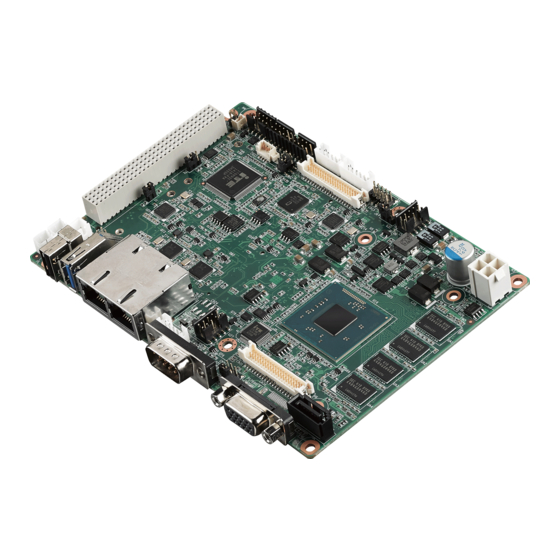
- Page 1 User Manual PCM-9365 ® ® ™ Intel Celeron N2930 & Atom E3825, 3.5" SBC, 2GB/4GB On-board Memory, VGA, 48-bit LVDS, 2GbE, Mini PCIe, PCI-104, SUSI 4...
- Page 2 No part of this manual may be reproduced, copied, translated or transmitted in any form or by any means without the prior written permission of Advantech Co., Ltd. Information provided in this manual is intended to be accurate and reliable. How- ever, Advantech Co., Ltd.
- Page 3 Because of Advantech’s high quality-control standards and rigorous testing, most of our customers never need to use our repair service. If an Advantech product is defec- tive, it will be repaired or replaced at no charge during the warranty period. For out- of-warranty repairs, you will be billed according to the cost of replacement materials, service time and freight.
-
Page 4: Declaration Of Conformity
Please use the public collection system to return, recycle, or treat them in compliance with the local regulations. Technical Support and Assistance Visit the Advantech website at http://support.advantech.com where you can find the latest information about the product. Contact your distributor, sales representative, or Advantech's customer service center for technical support if you need additional assistance. -
Page 5: Packing List
Packing List Before you begin installing your card, please make sure that the following materials have been shipped: 1 x PCM-9365 SBC 1 x SATA Cable 32cm (p/n: 1700008941) 1 x SATA Power Cable 35cm (p/n: 1700018785) ... - Page 6 PCM-9365 User Manual...
-
Page 7: Table Of Contents
Electrical Specifications ..............4 1.2.5 Environmental ................4 Block Diagram................... 5 Board layout: dimensions................6 Figure 1.1 PCM-9365 Mechanical Drawing (Top Side) ....6 Figure 1.2 PCM-9365 Mechanical Drawing (Bottom Side) ..7 Figure 1.3 PCM-9365 Mechanical Drawing (Coastline)....7 Chapter Installation..........9 Jumpers &... - Page 8 1st MB Memory Map................68 Table B.2: 1st MB Memory Map ..........68 Interrupt Assignments ................69 Table B.3: Interrupt assignments..........69 Appendix C EC Watchdog Timer Sample Code .. 71 EC Watchdog Timer sample code ............72 PCM-9365 User Manual viii...
-
Page 9: Chapter 1 General Information
Chapter General Information This chapter gives background information on the PCM-9365. Sections include: Introduction Specifications Block diagram Board layout and dimensions... -
Page 10: Introduction
Introduction PCM-9365 is 3.5" form factor (146 x 102 mm) and powered by the latest generation ® ® of Intel Celeron N2930 and Atom™ E3825 processors which have low power fea- tures but also good performance computing, especially for multimedia capabilities compared to earlier generations. -
Page 11: Os Support
UEFI is needed, that can be done by T-P/N 1.2.2 OS support PCM-9365 supports Win8, Win7, WES8, WES7, WEC7, Linux kernel 3.x, VxWorks 6.9.3.3, Android Kit Kat 4.4 Win7 only supports Legacy mode and Win8 for UEFI mode. -
Page 12: Mechanical Specifications
Normal discharge capacity: 210 mAh 1.2.5 Environmental Operating Temperature: 0 ~ 60°C (32 ~ 140°F) Operating Humidity: 40°C @ 85% RH Non-Condensing Storage Temperature: Storage temperature: -40~85°C Storage Humidity: Relative humidity: 95% @ 60°C PCM-9365 User Manual... -
Page 13: Block Diagram
1 x USB2.0 USB2.0 Bridge IT8892 PCI-104 PCIex1 1 x USB3.0 USB2.0/USB3.0 USB HUB 2 x USB2.0 ALC888S-VD2-GR USB2.0 HD Audio USB2.0 USB2514B Line-in/out 8-bit GPIO Mic-in ITE 8528 SMBus/ I COM 2/3/4: RS-232 ITE 8768 COM1: RS-232/422/485 PCM-9365 User Manual... -
Page 14: Board Layout: Dimensions
Board layout: dimensions Figure 1.1 PCM-9365 Mechanical Drawing (Top Side) PCM-9365 User Manual... -
Page 15: Figure 1.2 Pcm-9365 Mechanical Drawing (Bottom Side)
BOT H<10 Figure 1.2 PCM-9365 Mechanical Drawing (Bottom Side) Figure 1.3 PCM-9365 Mechanical Drawing (Coastline) PCM-9365 User Manual... - Page 16 PCM-9365 User Manual...
-
Page 17: Chapter 2 Installation
Chapter Installation This chapter explains the setup procedures of the PCM-9365 hard- ware, including instructions on setting jumpers and connecting peripherals, switches and indica- tors. Be sure to read all safety pre- cautions before you begin the installation procedure. -
Page 18: Jumpers & Switches
Jumpers & Switches The PCM-9365 has a number of jumpers that allow you to configure your system to suit your application. The table below lists the functions of the various jumpers. Table 2.1: Jumpers & Switches Auto Power On PCI-104 VIO... -
Page 19: Locating Connectors
Table 2.2: Connectors CN33 SMBus CN37 COM3/COM4 PCI-104 -12V Input * represents default configuration Locating Connectors Figure 2.1 PCM-9365 Connector Locations (Top Side) PCM-9365 User Manual... -
Page 20: Setting Jumpers
Figure 2.2 PCM-9365 Connector Locations (Bottom Side) Setting Jumpers You may configure your card to match the needs of your application by setting jump- ers. A jumper is a metal bridge used to close an electric circuit. It consists of two metal pins and a small metal clip (often protected by a plastic cover) that slides over the pins to connect them. -
Page 21: Pci-104 Vio (J2)
Function (1-2) (2-3)* +3.3V (default) 2.4.3 LVDS1 Power (J4) Table 2.5: LVDS1 Power (J4) Setting Function (1-3)* +3.3V (default) (3-5) (3-4) +12V 2.4.4 LVDS2 Power (J5) Table 2.6: LVDS2 Power (J5) Setting Function (1-3)* +3.3V (default) (3-5) PCM-9365 User Manual... -
Page 22: Clear Cmos (J6)
LVDS1 Pull-low to GND (default, JEIDA or VESA based on panel definition) (2-4) LVDS2 Pull-high to +3.3V (JEIDA or VESA based on panel defini- tion) (4-6)* LVDS2 Pull-low to GND (default, JEIDA or VESA based on panel definition) PCM-9365 User Manual... -
Page 23: Chapter 3 Ami Bios Setup
Chapter AMI BIOS Setup... - Page 24 With the AMIBIOS Setup program, you can modify BIOS settings and control the var- ious system features. This chapter describes the basic navigation of the PCM-9365 BIOS setup screens. AMI BIOS ROM has a built-in Setup program that allows users to modify the basic system configuration.
-
Page 25: Entering Setup
BIOS supports your CPU. If there is no number assigned to the patch code, please contact an Advantech application engineer to obtain an up-to-date patch code file. This will ensure that your CPU‘s system status is valid. -
Page 26: Advanced Bios Features Setup
3.1.2 Advanced BIOS Features Setup Select the Advanced tab from the PCM-9365 setup screen to enter the Advanced BIOS Setup screen. You can select any of the items in the left frame of the screen, such as CPU Configuration, to go to the sub menu for that item. You can display an Advanced BIOS Setup option by highlighting it using the <Arrow>... - Page 27 OS. ACPI Sleep State Select the highest ACPI sleep state the system will enter when the SUSPEND button is pressed. Lock Legacy Resources Enables or Disables Lock of Legacy Resources PCM-9365 User Manual...
- Page 28 Set Parameters of Serial Port 1 (COM1). Serial Port 2 Configuration Set Parameters of Serial Port 2 (COM2). Serial Port 3 Configuration Set Parameters of Serial Port 3 (COM3). Serial Port 4 Configuration Set Parameters of Serial Port 4 (COM4). PCM-9365 User Manual...
- Page 29 This item allows users to set backlight mode. EC Power Saving Mode This item allows users to set the board’s power saving mode when off. EC Watch Dog Function This item allows users to select the EC watchdog timer. PCM-9365 User Manual...
- Page 30 3.1.2.4 S5 RTC Wake Settings Wake system from S5 Enable or disable System wake on alarm event. Select FixedTime, system will wake on the hr:min:sec specified. PCM-9365 User Manual...
- Page 31 Serial Port Console Redirection Console Redirection This item allows users to enable or disable console redirection for Microsoft Windows Emergency Management Services (EMS). Console Redirection This item allows users to configuration console redirection detail settings. PCM-9365 User Manual...
- Page 32 OS (Windows Server 2003 SP1, Windows XP SP2, SuSE Linux 9.2, RedHat Enterprise 3 Update 3.) Intel Virtualization Technology When enabled, a VMM can utilize the additional hardware capabilities provided by Vanderpool Technology. Power Technology Enable the power management features. PCM-9365 User Manual...
- Page 33 3.1.2.7 PPM Configuration CPU C state Report Enable/Disable CPU C state report to OS. Max CPU C-state This option controls Max C state that the processor will support. S0ix Enable/Disable CPU S0ix state. PCM-9365 User Manual...
- Page 34 SATA Speed Support Gen1 or Gen2. SATA ODD Port SATA ODD is Port0 or Port1. SATA Mode Select IDE / AHCI. Serial-ATA Port 0 / Port1 Enable / Disable Serial ATA Port0 / Port1. PCM-9365 User Manual...
- Page 35 Storage Controls the execution of UEFI and Legacy Storage OpROM. Video Controls the execution of UEFI and Legacy Video OpROM. Other PCI devices Determines OpROM execution policy for devices other than Network, Storage, or Video. PCM-9365 User Manual...
- Page 36 Maximum time the device will take before it properly reports itself to the Host Controller. 'Auto' uses default value: for a Root port it is 100 ms, for a Hub port the delay is taken from Hub descriptor. PCM-9365 User Manual...
- Page 37 3.1.2.11 Security Configuration TXE HMRFPO Disable TXE Firmware Update TXE EOP Message Send EOP Message Before Enter OS TXE Unconfiguration Perform Revert TXE settings to factory defaults PCM-9365 User Manual...
-
Page 38: Chipset Configuration
3.1.3 Chipset Configuration North Bridge Details for North Bridge items. South Bridge Details for South Bridge items. PCM-9365 User Manual... - Page 39 3.1.3.1 North Bridge Intel IGD Configuration Config Intel IGD Settings. LCD Control Config LCD Setting. Max TOLUD Maximum Value of TOLUD. PCM-9365 User Manual...
- Page 40 Select DVMT 5.0 Total Graphic Memory size used by the Internal Graphics Device. Aperture Size Select the Aperture Size. DOP CG Enable/Disable DOP clock gating. GTT Size Select the GTT Size IGD Thermal Enable/Disable IGD Thermal. Spread Spectrum clock Enable/Disable Spread Spectrum clock. PCM-9365 User Manual...
- Page 41 Secondary boot display selection will appear based on your selection. VGA modes will be supported only on primary display. LVDS / LVDS 2 Panel Type This item allow user to select LVDS panel type. PCM-9365 User Manual...
- Page 42 Select AC power state when power is re-applied after a power failure. Serial IRQ Mode Configure Serial IRQ Mode. Global SMI Lock Enable or Disable SMI lock. BIOS Read/Write Protection Enable or Disable BIOS SPI region read/write protect. PCM-9365 User Manual...
- Page 43 Enabled = Azalia will be unconditionally Enabled. Auto = Azalia will be enabled if present disabled otherwise. Azalia HDMI Codec Enable/Disable internal HDMI codec for Azalia HDMI Port B Enable/Disable HDMI Port B HDMI Port C Enable/Disable HDMI Port C PCM-9365 User Manual...
- Page 44 Control the USB EHCI (USB 2.0) functions. One EHCI controller must always be enabled. USB Per Port Control Control each of the USB ports (0~3). Enable: Enable USB per port; Disable: Use USB port X settings. PCM-9365 User Manual...
- Page 45 3.1.3.7 PCI Express Configuration PCI Express Port0 / Port2 Enable or Disable the PCI Express Port0 / Port 2 in the Chipset. Speed Configure PCIe Port Speed. PCM-9365 User Manual...
-
Page 46: Security
3.1.4 Security Select Security Setup from the PCM-9365 Setup main BIOS setup menu. All Security Setup options, such as password protection and virus protection are described in this section. To access the sub menu for the following items, select the item and press <Enter>:... -
Page 47: Boot
This means the default boot selec- tion is not automatically started by the firmware. Bootup NumLock State Select the keyboard NumLock state. Quiet Boot Enables or disables Quiet Boot option. Boot Option #1 Sets the system boot order. PCM-9365 User Manual... -
Page 48: Save & Exit
This item allows you to save the changes done so far as user defaults. Restore User Defaults This item allows you to restore the user defaults to all the options. Boot Override Boot device select can override your boot priority. PCM-9365 User Manual... -
Page 49: Appendix A Pin Assignments
Appendix Pin Assignments This appendix contains informa- tion of a detailed or specialized nature. Sections include: Jumper and Connector Tables... -
Page 50: Jumper List
PIN HEADER 3x1P 2.0mm 180D(M) DIP 2000-13 WS Setting Function (1-2) (2-3)* +3.3V LCD Power Part Number 1653003260 Footprint HD_3x2P_79 Description PIN HEADER 3x2P 2.0mm 180D(M) SMD 21N22050 Setting Function (1-3)* +3.3V (3-5) (3-4) +12V LCD Power Part Number 1653003260 Footprint HD_3x2P_79 PCM-9365 User Manual... - Page 51 Pull-High to +V3.3(JEIDA or VESA base on panel definition) (3-5)* Pull-Low to GND (JEIDA or VESA base on panel definition) (2-4) Pull-High to +V3.3(JEIDA or VESA base on panel definition) (4-6)* Pull-Low to GND (JEIDA or VESA base on panel definition) PCM-9365 User Manual...
-
Page 52: Connector Pin Definition
12V Power Input Part Number 1655004509-01 Footprint WF_2x2P_165_BOX_D Description ATX PWR Conn. 2x2P 4.2mm 180D(M) DIP 740-81-04GW Pin Name +12V +12V Battery Part Number 1655902032 Footprint WHL2V-125 Description WAFER BOX 2P 1.25mm 180D(M) DIP 53047-0210 Pin Name PCM-9365 User Manual... - Page 53 1654009557 Footprint FPC24H-05M Description FFC/FPC Conn. 24P 0.5mm 90D(F) SMD 52435-2471 Pin Name EC_KSI7 EC_KSI6 EC_KSI5 EC_KSI4 EC_KSI3 EC_KSI2 EC_KSI1 EC_KSI0 EC_KSO15 EC_KSO14 EC_KSO13 EC_KSO12 EC_KSO11 EC_KSO10 EC_KSO9 EC_KSO8 EC_KSO7 EC_KSO6 EC_KSO5 EC_KSO4 EC_KSO3 EC_KSO2 EC_KSO1 EC_KSO0 PCM-9365 User Manual...
- Page 54 Footprint WF_2P_79_BOX_R1_D Description WAFER BOX 2P 2.0mm 180D(M) DIP A2001WV2-2P Pin Name RESET# GPIO Part Number 1653004099 Footprint HD_5x2P_79_23N685B-10M10 Description BOX HEADER 5x2P 2.00mm 180D(M) SMD 23N685B-10M10 Pin Name GPIO4 GPIO0 GPIO5 GPIO1 GPIO6 GPIO2 GPIO7 GPIO3 PCM-9365 User Manual...
- Page 55 Part Number 1654000055 Footprint DBVGA-VF5MS Description D-SUB Conn. 15P 90D(F) DIP 070242FR015S200ZU Pin Name GREEN BLUE DDAT HSYNC VSYNC DCLK NL/HDMI_19H Part Number 1654011175-01 Footprint HDMI_19P_QJ51191-LFB4-7F Description HDMI Conn. 19P 0.5mm 90D(F) SMD QJ51191-LFB4-7F HDMI_TX2+ PCM-9365 User Manual...
- Page 56 HDMI_HPD SATA Part Number 1654004659 Footprint SATA_7P_WATM-07DBN4A3B8UW_D Description Serial ATA 7P 1.27mm 180D(M) DIP WATM-07DBN4A3B8 Pin Name CN10 HDD & PWR LED Part Number 1655306020 Footprint WHL6V-2M Description WAFER BOX 6P 2.0mm 180D(M) DIP A2001WV2-6P Pin Name PCM-9365 User Manual...
- Page 57 SATA Power Part Number 1655001154 Footprint WF_4P_98_BOX_R1_D Description WAFER BOX 4P 2.50mm 180D(M) DIP 24W1170-04S10-01 Pin Name +12V CN12 Mini PCIE Part Number 1654002538 Footprint MINIPCIE_HALF_PICO_ITX Description MINI PCI E 52P 6.8mm 90D SMD AS0B226-S68Q-7H Pin Name WAKE# PCM-9365 User Manual...
- Page 58 +3.3VSB +1.5V UIM_PWR UIM_DATA REFCLK- UIM_CLK REFCLK+ UIM_RESET UIM_VPP W_DISABLE# PERST# PERn0 +3.3VSB PERp0 +1.5V SMB_CLK PETn0 SMB_DAT PETp0 USB D- USB D+ +3.3VSB +3.3VSB +1.5V PCM-9365 User Manual...
- Page 59 +3.3VSB CN13 mSATA Part Number 1654002538 Footprint MINIPCIE_HALF_PICO_ITX Description MINI PCI E 52P 6.8mm 90D SMD AS0B226-S68Q-7H Pin Name +3.3V +1.5V PCM-9365 User Manual...
- Page 60 +3.3V +1.5V SMB_CLK SMB_DAT USB D- USB D+ +3.3V +3.3V +1.5V +3.3V CN14 Internal USB Part Number 1653005260 Footprint HD_5x2P_79_N10 Description PIN HEADER 2x5P 2.0mm 180D(M) SMD 21N22050 Pin Name A_D- B_D- A_D+ PCM-9365 User Manual...
- Page 61 HD_5x2P_79_N10 Description PIN HEADER 2x5P 2.0mm 180D(M) SMD 21N22050 Pin Name A_D- B_D- A_D+ B_D+ CN16 External USB3.0 Part Number 1654010026 Footprint USB_9P_UEA3119C-4FB1-4F Description USB 3.0 CONN 9P 90D(F) DIP UEA3119C-4FB1-4 Pin Name SSRX- SSRX+ SSTX- SSTX+ PCM-9365 User Manual...
- Page 62 Footprint USB_4P_22-0403N-4-1T-R Description USB CONN. 4P 90D(F) DIP 22-0403N-4-1T-R Pin Name CN18 COM1 Part Number 1654000056 Footprint DBCOM-VM5MS Description D-SUB Conn. 9P 90D(M) DIP 070241MR009S200ZU Pin Name DCD# DTR# DSR# RTS# CTS# CN19 COM2 Part Number 1653004099 PCM-9365 User Manual...
- Page 63 1652002996 Footprint RJ45_14P_RTA-195AAK1A Description PHONE JACK RJ45 14P 90D(M) DIP RTA-195AAK1A Pin Name LAN1_MDI0+ LAN1_MDI0- LAN1_MDI1+ LAN1_MDI1- LAN1CONN LAN1_GND LAN1_MDI2+ LAN1_MDI2- LAN1_MDI3+ LAN1_MDI3- LAN1_ACT# +V3.3_VDD_LAN1 LAN1_LINK100# LAN1_LINK1000# CN23 LAN1 & LAN2 (Dual LAN connector) Part Number 1652003274 PCM-9365 User Manual...
- Page 64 LAN2_MDI1- LAN2CONN LAN2_GND LAN2_MDI2+ LAN2_MDI2- LAN2_MDI3+ LAN2_MDI3- LAN2_ACT# +V3.3_VDD_LAN2 LAN2_LINK100# LAN2_LINK1000# CN24 Internal LAN LED Part Number 1653004260 Footprint HD_4x2_79 Description PIN HEADER 4x2P 2.0mm 180D(M) SMD 21N22050 Pin Name +V3.3SB +V3.3SB LAN1_ACT# LAN2_ACT# LAN1_LINK100# LAN2_LINK100# LAN1_LINK1000# PCM-9365 User Manual...
- Page 65 LAN2_MDI0+ LAN2_MDI0- LAN2_MDI1+ LAN2_MDI1- LAN2CONN LAN2_GND LAN2_MDI2+ LAN2_MDI2- LAN2_MDI3+ LAN2_MDI3- LAN2_ACT# +V3.3_VDD_LAN2 LAN2_LINK100# LAN2_LINK1000# CN26 Audio Part Number 1653004099 Footprint HD_5x2P_79_23N685B-10M10 Description BOX HEADER 5x2P 2.00mm 180D(M) SMD 23N685B-10M10 Pin Name LOUTR LINR LOUTL LINL MIC1R MIC1L PCM-9365 User Manual...
- Page 66 AD11 AD14 +3.3V SERR# PA10 PA11 STOP# PA12 +3.3V PA13 FRAME# PA14 PA15 AD18 PA16 AD21 PA17 +3.3V PA18 IDSEL0 PA19 AD24 PA20 PA21 AD29 PA22 PA23 REQ0# PA24 PA25 GNT1# PA26 PA27 CLK2 PA28 PA29 +12V PCM-9365 User Manual...
- Page 67 AD30 PB23 PB24 REQ2# PB25 VI/O (+5V or +3.3V) PB26 CLK0 PB27 PB28 INTD# PB29 INTA# PB30 REQ3# AD01 AD04 AD08 AD10 AD15 PC10 +3.3V PC11 LOCK# PC12 PC13 IRDY# PC14 +3.3V PC15 AD17 PC16 PC17 AD22 PCM-9365 User Manual...
- Page 68 PD11 PD12 DEVSEL# PD13 +3.3V PD14 C/BE2# PD15 PD16 AD19 PD17 +3.3V PD18 IDSEL2 PD19 IDSEL3 PD20 PD21 AD27 PD22 AD31 PD23 VI/O (+5V or +3.3V) PD24 GNT0# PD25 PD26 CLK1 PD27 PD28 RESET# PD29 INTC# PD30 PCM-9365 User Manual...
- Page 69 ENABKL CN29 48 bits LVDS Panel1 Part Number 1653920200 Footprint SPH20X2 Description B/B Conn. 40P 1.25mm 90D SMD DF13-40DP-1.25V(91) Pin Name +5V or +3.3V +5V or +3.3V +5V or +3.3V +5V or +3.3V LVDS0_D0- LVDS1_D0- LVDS0_D0+ LVDS1_D0+ PCM-9365 User Manual...
- Page 70 LVDS1_D1+ LVDS0_D2- LVDS1_D2- LVDS0_D2+ LVDS1_D2+ LVDS0_CLK- LVDS1_CLK- LVDS0_CLK+ LVDS1_CLK+ LVDS0_D3- LVDS1_D3- LVDS0_D3+ LVDS1_D3+ LVDS1_VCCON CN30 Inverter Power Output2 Part Number 1655000453 Footprint WHL5V-2M-24W1140 Description WAFER BOX 2.0mm 5P 180D(M) DIP WO/Pb JIH VEI Pin Name +12V ENABKL PCM-9365 User Manual...
- Page 71 Description B/B Conn. 40P 1.25mm 90D SMD DF13-40DP-1.25V(91) Pin Name +5V or +3.3V +5V or +3.3V +5V or +3.3V +5V or +3.3V LVDS0_D0- LVDS1_D0- LVDS0_D0+ LVDS1_D0+ LVDS0_D1- LVDS1_D1- LVDS0_D1+ LVDS1_D1+ LVDS0_D2- LVDS1_D2- LVDS0_D2+ LVDS1_D2+ LVDS0_CLK- LVDS1_CLK- LVDS0_CLK+ PCM-9365 User Manual...
- Page 72 Part Number 1655904020 Footprint FPC4V-125M Description WAFER 4P 1.25mm 180D(M) SMD 85205-04001 Pin Name SMB_DAT SMB_CLK CN37 COM3/COM4 Part Number 1653004793 Footprint HD_10x2P_79_23N685B-20M10 Description BOX HEADER 10x2P 2.0mm 180D(M)SMD 23N685B-20M10B Pin Name DCD3# DSR3# RXD3 RTS3# TXD3 PCM-9365 User Manual...
- Page 73 CTS3# DTR3# RI3# DCD4# DSR4# RXD4 RTS4# TXD4 CTS4# DTR4# RI4# PCI-104 -12V Input Part Number 1653002101 Footprint HD_2x1P_79_D Description PIN HEADER 2*1P 180D(M)SQUARE 2.0mm DIP W/O Pb Pin Name -12V PCM-9365 User Manual...
- Page 74 PCM-9365 User Manual...
-
Page 75: Appendix B System Assignments
Appendix System Assignments This appendix contains informa- tion of a detailed nature. Sections include: System I/O Ports 1st MB Memory Map Interrupt Assignments... -
Page 76: System I/O Ports
Addr. Range (Hex) Device A0000h - BFFFFh Intel® HD Graphics A0000h - BFFFFh PCI Bus C0000h - DFFFFh PCI Bus E0000h - FFFFFh PCI Bus D0400000 – D05FFFFF Intel® Trusted Execution Engine Interface E0000000 - FEFFFFFF System resources PCM-9365 User Manual... -
Page 77: Interrupt Assignments
IRQ6 Available IRQ7 Communications Port (COM3) / iManager WatchDog IRQ IRQ8 Internal RTC or HPET IRQ9 Microsoft ACPI-Compliant System IRQ10 Available IRQ11 Communications Port (COM4) IRQ12 Available IRQ13 Numeric data processor IRQ14 SATA controller IRQ15 SATA controller PCM-9365 User Manual... - Page 78 PCM-9365 User Manual...
-
Page 79: Appendix Cec Watchdog Timer Sample Code
Appendix EC Watchdog Timer Sample Code... -
Page 80: Ec Watchdog Timer Sample Code
;Write EC HW ram. out dx,al mov dx, EC_Data_Port mov al, 57h ;Watch dog event flag. out dx,al mov dx, EC_Data_Port mov al, 04h ;Reset event. out dx,al mov dx, EC_Command_Port mov al,28h ;Start WDT function. out dx,al .exit PCM-9365 User Manual... - Page 81 PCM-9365 User Manual...
- Page 82 No part of this publication may be reproduced in any form or by any means, electronic, photocopying, recording or otherwise, without prior written permis- sion of the publisher. All brand and product names are trademarks or registered trademarks of their respective companies. © Advantech Co., Ltd. 2015...
Need help?
Do you have a question about the PCM-9365 and is the answer not in the manual?
Questions and answers