Table of Contents
Advertisement
Quick Links
Z8F80306082
EB 2ED2410 3M/3D Family
Evaluation mother/daughterboards
About this document
Scope and purpose
This user guide is intended to enable users to easily "plug and play" evaluation board EB 2ED2410 3M
"motherboard" with its daughterboards:
•
EB 2ED2410 3D 1BCD
•
EB 2ED2410 3D 1BCS
•
EB 2ED2410 3D 1BCDP
•
EB 2ED2410 3D 1BCSP
and assesses the features it offers.
This document describes functionalities, set-up protections, layout choices that have been implemented, and
shows how to test them.
Intended audience
This document is intended for qualified electronic engineers who need a smart N-channel MOSFET gate driver
with integrated bi-directional current sense, wire protection and strong gate drive capability for automotive or
industrial fail safe and fail operational applications.
User guide
www.infineon.com
Please read the Important notice and the Safety precautions and the Warnings
page 1 of 30
Rev.1.00
2022-08-05
Advertisement
Table of Contents

Related Manuals for Infineon EB 2ED2410 3D 1BCD


Summarization of Contents
1 Overview
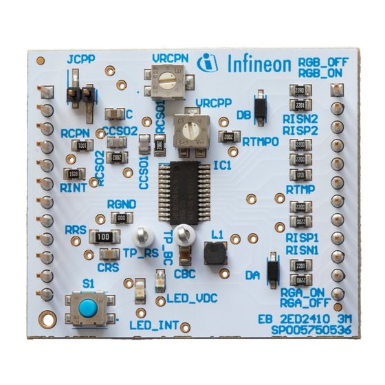
1.1 Motherboard EB 2ED2410 3M
Details the EB 2ED2410 3M motherboard's features, components, and diagnostic capabilities.
1.2 Daughterboards EB 2ED2410 3D
Describes the EB 2ED2410 3D daughterboards, their topologies, and connection to the motherboard.
1.3 High level diagrams
Presents block diagrams of the motherboard and daughterboards, illustrating interconnections and signal flow.
2 Connecting and operating the board
2.1 Boards assembly
Step-by-step guide for physically connecting the motherboard and daughterboards for initial setup.
2.2 Power connection
Instructions and diagrams for properly connecting power sources to the evaluation boards.
2.3 Pin assignment and pin ratings
Details pin assignments and electrical ratings for all headers and connectors on the evaluation board.
2.4 Jumpers
Explains the function and usage of jumpers for configuring board features and operational modes.
2.5 Voltage ranges
Specifies acceptable voltage ranges for motherboard and daughterboards as per ISO16750-2.
2.6 Operation to avoid
Highlights critical operational restrictions and actions to prevent damage to the 2ED2410-EM.
2.7 Quiescent current
Details test setup and typical values for quiescent current in SLEEP, IDLE, and ON modes.
3 Switching behavior
3.1 Basic switching
Illustrates switching waveforms from SLEEP to IDLE and IDLE to ON modes.
3.2 Short-circuit event
Demonstrates response to a short circuit, triggering SAFESTATE mode and the INT signal.
3.3 Pre-charge for capacitive loads (daughterboards -1BCSP / -1BCDP only)
Explains pre-charge circuitry for specific daughterboards to manage inrush current for capacitive loads.
4 Protections
4.1 2ED2410-EM short-circuit protection
Details internal short-circuit protection, its settings, and current limits based on ENABLE voltage.
4.2 I-t wire protection with comparator CP
Describes I-t wire protection, adjustable settings using VRCPN and VRCPP potentiometers.
4.3 Overtemperature protection with comparator CP
Explains overtemperature check via TMPO to CPP connection and threshold setting.
5 Electrical schematic
5.1 BOM
Provides the Bill of Materials (BOM) listing all components for the EB 2ED2410 3M evaluation board.
5.2 Electrical diagrams
Presents the detailed electrical schematic diagrams for the EB 2ED2410 3M evaluation board.
6 PCB details
6.1 Layers EB 2ED2410 3M
Illustrates the layer stack-up and signal routing for the EB 2ED2410 3M PCB.
6.2 Layers EB 2ED2410 3D 1BCD
Shows top and bottom layer signal paths and layout for the EB 2ED2410 3D 1BCD daughterboard.
6.3 Layers EB 2ED2410 3D 1BCDP
Displays top and bottom layer signal paths and layout for the EB 2ED2410 3D 1BCDP daughterboard.
Need help?
Do you have a question about the EB 2ED2410 3D 1BCD and is the answer not in the manual?
Questions and answers