Table of Contents
Advertisement
Quick Links
Z8F80306082
EB 2ED2410 3M/3D Family
Evaluation mother/daughterboards
About this document
Scope and purpose
This user guide is intended to enable users to easily "plug and play" evaluation board EB 2ED2410 3M
"motherboard" with its daughterboards:
•
EB 2ED2410 3D 1BCD
•
EB 2ED2410 3D 1BCS
•
EB 2ED2410 3D 1BCDP
•
EB 2ED2410 3D 1BCSP
and assesses the features it offers.
This document describes functionalities, set-up protections, layout choices that have been implemented, and
shows how to test them.
Intended audience
This document is intended for qualified electronic engineers who need a smart N-channel MOSFET gate driver
with integrated bi-directional current sense, wire protection and strong gate drive capability for automotive or
industrial fail safe and fail operational applications.
User guide
www.infineon.com
Please read the Important notice and the Safety precautions and the Warnings
page 1 of 30
Rev.1.00
2022-08-05
Advertisement
Table of Contents

Subscribe to Our Youtube Channel
Related Manuals for Infineon EB 2ED2410 3M Series


Summary of Contents for Infineon EB 2ED2410 3M Series
-
Page 1: About This Document
User guide Please read the Important notice and the Safety precautions and the Warnings Rev.1.00 www.infineon.com page 1 of 30 2022-08-05... -
Page 2: Table Of Contents
EB 2ED2410 3M/3D Family Evaluation mother/daughterboards Table of contents Table of contents About this document ........................1 Table of contents ..........................2 Overview ..........................3 Motherboard EB 2ED2410 3M ........................3 Daughterboards EB 2ED2410 3D ......................4 1.2.1 Daughterboards current rating......................5 High level diagrams .......................... -
Page 3: Overview
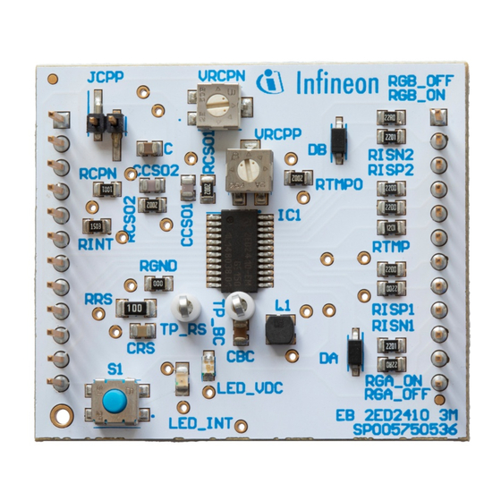
Note: Failure mode analysis of connected MOSFET needs a specific set-up: it is not treated in this document and will be described in a separate Infineon Application Note The gate driver is protected against overvoltage by a 100 nF (C ) plus optional 1 W zener (Z1) on pin VS. -
Page 4: Daughterboards Eb 2Ed2410 3D
Common source with pre-charge Mandatory connection with pre-charge circuit to load side Figure 2 Top (main switch path) & back view of daughterboards EB 2ED2410 3D-1BCD and -1BCDP Table 3 Infineon parts used in EB 2ED2410-EM 3D Type Reference Comment MOSFET... -
Page 5: Daughterboards Current Rating
EB 2ED2410 3M/3D Family Evaluation mother/daughterboards Overview 1.2.1 Daughterboards current rating The daughterboards are designed for continuous 20 A operation, 30 A for 10 minutes and 60 A for one minute without the I-t wire protection. See Chapter 4.2 for I-t wire protection adjustment. Short-circuit limit is by default using 5 V Enable from TLE42926GV50 @ 80 A, see Chapter 4.1 for details. - Page 6 EB 2ED2410 3M/3D Family Evaluation mother/daughterboards Overview EB 2ED2410 3D 1B D hunt Figure 4 Overview of daughterboard -1BCD EB 2ED2410 3D 1B D hunt re charge path evel shi er re charge Figure 5 Overview of daughterboard -1BCDP User guide 6 of 30 Rev.1.00 2022-08-05...
- Page 7 EB 2ED2410 3M/3D Family Evaluation mother/daughterboards Overview EB 2ED2410 3D 1B hunt B T 4 21 Figure 6 Overview of daughterboard -1BCS EB 2ED2410 3D 1B hunt B T 4 21 re charge path evel shi er Figure 7 Overview of daughter board -1BCSP User guide 7 of 30 Rev.1.00...
-
Page 8: Connecting And Operating The Board
EB 2ED2410 3M/3D Family Evaluation mother/daughterboards Connecting and operating the board onnecting and operating the board This chapter describes how to connect the motherboard with the daughterboard and gives a non-exhaustive list of actions to avoid in order to keep 2ED2410-EM and the board operational. Boards assembly Step1: Bring the boards together, so top overlay (text) can be read on both boards. -
Page 9: Power Connection
EB 2ED2410 3M/3D Family Evaluation mother/daughterboards Connecting and operating the board ower connection Refer to table 2 for connection options for each daughterboard. Figure 10 Power connection diagrams with 3D-1BCD Figure 11 Power connection diagram with 3D-1BCDP, 3D-1BCS, 3D-1BCSP LOAD: Electronic loads as well as classical passive elements are usable. - Page 10 EB 2ED2410 3M/3D Family Evaluation mother/daughterboards Connecting and operating the board The right pin headers allow readings of all signals from and to the MOSFET and shunt for observation purposes, for example an oscilloscope. Figure 12 Pin header details with top view Refer to 2ED2410-EM datasheet [1] for detailed operating modes in Chapter 5.1 Operating modes.
-
Page 11: Jumpers
EB 2ED2410 3M/3D Family Evaluation mother/daughterboards Connecting and operating the board Jumpers Two 2 mm jumpers are present on the board. Table 5 Jumpers Location Comment JCPP On the top Enables or disables the I-t wire protection. When taken off, RCPP and C are disconnected from CSO2. -
Page 12: Quiescent Current
EB 2ED2410 3M/3D Family Evaluation mother/daughterboards Connecting and operating the board Quiescent current Quiescent current of 2ED2410-EM can easily be verified with back-to-back demoboard. The quiescent current is measured in SLEEP mode, the consumption is measured in IDLE mode and in ON mode in open load (to simulate no current drawn by load and consider only the consumption by the driver itself). -
Page 13: Switching Behavior
EB 2ED2410 3M/3D Family Evaluation mother/daughterboards Switching behavior witching behavior Note: Values shown in this chapter are measured under lab conditions and will vary for different cooling conditions and setups, and samples used. Basic switching Next figure shows switching behavior from SLEEP to IDLE mode. As soon as V threshold is met, 2ED2410-EM powers up and the boost converter charges the driver supply C (monitored by V... -
Page 14: Short-Circuit Event
EB 2ED2410 3M/3D Family Evaluation mother/daughterboards Switching behavior Figure 18 Waveforms from ON to IDLE [Yellow V ; Green V ; Purple V ; Blue I LOAD hort circuit event Next figure shows switching behavior from ON to SAFESTATE mode. SAFESTATE mode is triggered here by a short circuit across the load resistor made by a loose wire, manually. -
Page 15: Pre-Charge For Capacitive Loads (Daughterboards -1Bcsp / -1Bcdp Only)
MOSFET is driven by a push-pull providing the boosted BC voltage to the M_pch MOSFET gate. This circuit is an example of circuit re-using the 2ED2410-EM boost converter (BC) voltage and small signal Infineon MOSFET BSS83P and 2N7002. Note: There is no specific protection for the resistor R_pwr (6W resistor, see BOM). - Page 16 EB 2ED2410 3M/3D Family Evaluation mother/daughterboards Switching behavior Waveform generator Pre-ch. starts Pre-ch. is off, main switch starts & V PRE-CH. 4 Ω LOAD 150ms max. Battery Figure 21 Test circuit of pre-charge control The figure below shows a 150 ms pre-charge of a capacitor C = 6.8 mF.
-
Page 17: Protections
EB 2ED2410 3M/3D Family Evaluation mother/daughterboards Protections rotections 2ED2410 EM short circuit protection Note: The EB 2ED2410-EM 3D boards are not designed for repetitive short-circuit operation. Short-circuit energy dissipation relies on MOSFET avalanche performance. Therefore the number of short- circuit cycles possible have to be calculated based on the customer’s short-circuit test set-up 2ED2410-EM has an internal short-circuit protection. -
Page 18: Overtemperature Protection With Comparator Cp
The following graph shows the I-t wire protection curve adjustment area (in orange color) with VRCPN and VRCPP given the default short-circuit value and components on EB 2ED2410 3M/3D (EiceDRIVER 2ED2410 Tool, ™ downloadable from the 2ED2410-EM website [3]or Infineon Development Center [4] in future). Figure 24 I-t wire setting range Overtemperature protection with comparator To simply check overtemperature protection, disconnect JCPP and connect TMPO pin header to CPP pin header with a jump wire. - Page 19 EB 2ED2410 3M/3D Family Evaluation mother/daughterboards Protections Connecting TMPO J1-3, directly to CPP J1-8 Figure 25 How to wire overtemperature protection The threshold of overtemperature can be set with V on CPN pin, same operation as I-t wire threshold. CP(REF) The below graph shows the implemented temperature curve in the EB 2ED2410 3M/3D boards, given V = 5 V, RTMP, RNTC and RTMPO as described in the BOM chap.
-
Page 20: Electrical Schematic
EB 2ED2410 3M/3D Family Evaluation mother/daughterboards Electrical schematic Electrical schematic 5.1.1 EB 2ED2410 3M Reference Description Designator 10 µF / 10 V Capacitor 1 µF / 25 V Capacitor 100 pF/10 V Capacitor CCSO1, CCSO2 100 nF / 100 V Capacitor CREG_in, CVS 4.7 µF / 10 V... -
Page 21: Eb 2Ed2410 3D 1Bcd Or 1Bcs
EB 2ED2410 3M/3D Family Evaluation mother/daughterboards Electrical schematic 5.1.2 EB 2ED2410 3D 1B D or 1B Reference Description Designator 973582101 - red Connector JA/BA, JB/BB BAV23C-Q Diode (1BCS only) MMSZ5245BT1G Zener Diode DA, DB TSW-112-07-G-S Connector J1, J2 973582101 Connector JA, JB IAUC120N06S5N011 MOSFET (N-Channel) -
Page 22: Electrical Diagrams
EB 2ED2410 3M/3D Family Evaluation mother/daughterboards Electrical schematic Electrical diagrams Figure 27 EB 2ED2410 3M User guide 22 of 30 Rev.1.00 2022-08-05... - Page 23 EB 2ED2410 3M/3D Family Evaluation mother/daughterboards Electrical schematic Figure 28 EB 2ED2410 3D 1BCD User guide 23 of 30 Rev.1.00 2022-08-05...
- Page 24 EB 2ED2410 3M/3D Family Evaluation mother/daughterboards Electrical schematic Figure 29 EB 2ED2410 3D 1BCDP User guide 24 of 30 Rev.1.00 2022-08-05...
-
Page 25: Pcb Details
EB 2ED2410 3M/3D Family Evaluation mother/daughterboards PCB details B details EB 2ED2410 3M PCB is a 4-layers, HTG-150 material board. EB 2ED2410 3M PCB is a 2-layers, HTG-150 material board. Figure 30 EB 2ED2410 3M PCB layers 4 * 35µm Figure 31 EB 2ED2410 3D PCB layers 2 * 70µm User guide... -
Page 26: Layers Eb 2Ed2410 3M
EB 2ED2410 3M/3D Family Evaluation mother/daughterboards PCB details ayers EB 2ED2410 3M Figure 32 Top layer signal [35 µm] and Bottom layer signal [35 µm] Figure 33 Mid layers Vref [35 µm] and GND [35 µm] User guide 26 of 30 Rev.1.00 2022-08-05... -
Page 27: Layers Eb 2Ed2410 3D 1Bcd
EB 2ED2410 3M/3D Family Evaluation mother/daughterboards PCB details ayers EB 2ED2410 3D 1B D Figure 34 Top Layer [70 µm] and bottom layer [70 µm] ayers EB 2ED2410 3D 1B D Figure 35 Top Layer [70µm] and bottom layer [70µm] User guide 27 of 30 Rev.1.00... -
Page 28: References
EB 2ED2410 3M/3D Family Evaluation mother/daughterboards References eferences EiceD I E ™ D 2ED2410-EM Datasheet, https://www.infineon.com/dgdl/Infineon-2ED2410-EM- DataSheet-v02_00-EN.pdf Getting started with 2ED2410-EM, https://www.infineon.com/dgdl/Infineon-2ED2410-EM- ApplicationNotes-v01_00-EN.pdf 2ED2410-EM website, https://www.infineon.com/cms/en/product/power/gate-driver-ics/automotive- gate-driver-ics/2ed2410-em/ Infineon Development Center, https://softwaretools.infineon.com/welcome User guide 28 of 30 Rev.1.00 2022-08-05... -
Page 29: Revision History
EB 2ED2410 3M/3D Family Evaluation mother/daughterboards References evision history Document Date of release Description of changes version V 1.00 2022-08-05 First release User guide 29 of 30 Rev.1.00 2022-08-05... - Page 30 With respect to any examples, hints or any typical 81726 Munich, Germany values stated herein and/or any information WARNINGS regarding the application of the product, Infineon Technologies hereby disclaims any and all Due to technical requirements products may contain warranties and liabilities of any kind, including dangerous substances.
Need help?
Do you have a question about the EB 2ED2410 3M Series and is the answer not in the manual?
Questions and answers