Table of Contents
Advertisement
Quick Links
Z8F80306082
EB 2ED2410 3M/3D Family
Evaluation mother/daughterboards
About this document
Scope and purpose
This user guide is intended to enable users to easily "plug and play" evaluation board EB 2ED2410 3M
"motherboard" with its daughterboards:
•
EB 2ED2410 3D 1BCD
•
EB 2ED2410 3D 1BCS
•
EB 2ED2410 3D 1BCDP
•
EB 2ED2410 3D 1BCSP
and assesses the features it offers.
This document describes functionalities, set-up protections, layout choices that have been implemented, and
shows how to test them.
Intended audience
This document is intended for qualified electronic engineers who need a smart N-channel MOSFET gate driver
with integrated bi-directional current sense, wire protection and strong gate drive capability for automotive or
industrial fail safe and fail operational applications.
User guide
www.infineon.com
Please read the Important notice and the Safety precautions and the Warnings
page 1 of 30
Rev.1.00
2022-08-05
Advertisement
Table of Contents

Related Manuals for Infineon EB 2ED2410 3D 1BCS


Summarization of Contents
Document Overview and Purpose
Scope and Purpose
Details the user guide's intent to facilitate easy plug-and-play evaluation of the EB 2ED2410 3M motherboard.
Intended Audience
Identifies the target audience as qualified electronic engineers requiring a smart N-channel MOSFET gate driver for automotive applications.
1 Overview of EB 2ED2410 Family
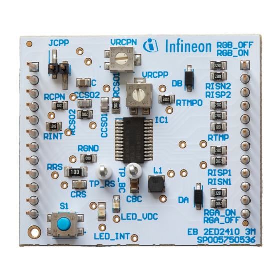
1.1 Motherboard EB 2ED2410 3M
Describes the EB 2ED2410 3M motherboard, its driver, control interface, and integrated protection logic.
1.2 Daughterboards EB 2ED2410 3D
Details the EB 2ED2410 3D daughterboards, featuring N-channel MOSFETs and options for pre-charge functionality.
1.3 High Level Diagrams
Presents diagrams illustrating motherboard and daughterboard connections for testing basic functionality.
2 Connecting and Operating the Board
2.1 Boards Assembly
Provides step-by-step instructions for physically assembling the motherboard and daughterboards.
2.2 Power Connection
Illustrates power connection diagrams and outlines guidelines for connecting boards to power sources and loads.
2.3 Pin Assignment and Ratings
Details pin header assignments, their functions, and crucial operational voltage and current ratings.
2.4 Jumpers
Explains the function and use of the two 2 mm jumpers present on the evaluation board.
2.5 Voltage Ranges
Outlines the supported voltage ranges for both the motherboard and the various daughterboards.
2.6 Operation to Avoid
Highlights critical operations to prevent, detailing potential damage to the 2ED2410-EM driver.
2.7 Quiescent Current Measurement
Describes the procedure and presents results for measuring quiescent current in SLEEP, IDLE, and ON modes.
3 Switching Behavior
3.1 Basic Switching Waveforms
Shows waveforms detailing the driver's transitions between SLEEP, IDLE, and ON operational modes.
3.2 Short-Circuit Event Response
Presents waveforms illustrating the driver's reaction to a short circuit, including SAFESTATE mode activation.
3.3 Pre-Charge for Capacitive Loads
Explains the pre-charge circuit's function and presents test results for managing inrush current with capacitive loads.
4 Board Protections
4.1 Short-Circuit Protection
Details the internal short-circuit protection of the 2ED2410-EM and its configurable set-up parameters.
4.2 I-t Wire Protection
Describes the I-t wire protection setup using the comparator CP, including adjustment possibilities.
4.3 Overtemperature Protection
Outlines the method to check overtemperature protection by linking TMPO pin to CPP pin.
5 Electrical Schematic
5.1 Bill of Materials (BOM)
Provides the comprehensive Bill of Materials for the EB 2ED2410 3M motherboard and daughterboards.
5.1.1 EB 2ED2410 3M BOM
Presents the detailed component list for the EB 2ED2410 3M motherboard.
5.1.2 EB 2ED2410 3D 1BCD/1BCS BOM
Lists the components for the EB 2ED2410 3D 1BCD and 1BCS daughterboard variants.
5.1.3 EB 2ED2410 3D 1BCDP/1BCSP BOM
Lists the components for the EB 2ED2410 3D 1BCDP and 1BCSP daughterboard variants.
5.2 Electrical Diagrams
Includes detailed schematic diagrams for the EB 2ED2410 3M motherboard.
6 PCB Details
6.1 EB 2ED2410 3M PCB Layers
Details the PCB layer structure for the EB 2ED2410 3M, including copper weight and layer types.
6.2 EB 2ED2410 3D 1BCD PCB Layers
Presents the PCB layer information for the EB 2ED2410 3D 1BCD daughterboard.
6.3 EB 2ED2410 3D 1BCDP PCB Layers
Presents the PCB layer information for the EB 2ED2410 3D 1BCDP daughterboard.
Need help?
Do you have a question about the EB 2ED2410 3D 1BCS and is the answer not in the manual?
Questions and answers