Table of Contents
Advertisement
Quick Links
UM3345
User manual
STM32WB09 Nucleo-64 board (MB1801 and MB2032)
Introduction
®
NUCLEO-WB09KE
is a Bluetooth
Low Energy wireless and ultra-low-power board embedding a powerful and ultra-low-power
®
radio compliant with the Bluetooth
Low Energy SIG specification v5.4.
®
The ARDUINO
Uno V3 connectivity support and the ST morpho headers allow the easy expansion of the functionality of the
STM32 Nucleo open development platform with a wide choice of specialized shields.
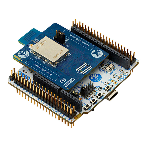
Figure 1.
NUCLEO-WB09KE global view
Picture is not contractual.
UM3345 - Rev 1 - July 2024
www.st.com
For further information contact your local STMicroelectronics sales office.
Advertisement
Table of Contents

Subscribe to Our Youtube Channel
Related Manuals for ST NUCLEO-WB09KE


Summary of Contents for ST NUCLEO-WB09KE
-
Page 1: Figure 1. Nucleo-Wb09Ke Global View
Low Energy SIG specification v5.4. ® The ARDUINO Uno V3 connectivity support and the ST morpho headers allow the easy expansion of the functionality of the STM32 Nucleo open development platform with a wide choice of specialized shields. Figure 1. -
Page 2: Features
USB Type-C ® – ARDUINO Uno V3 expansion connector – ST morpho headers for full access to all STM32 I/Os • Flexible power-supply options: ST-LINK USB V or external sources • On-board STLINK-V3EC debugger/programmer with USB re-enumeration capability: mass storage, Virtual COM port, and debug port •... -
Page 3: Ordering Information
UM3345 Ordering information Ordering information To order the NUCLEO-WB09KE board, refer to Table 1. Additional information is available from the datasheet and reference manual of the target STM32. Table 1. Ordering information Order code Board references Target STM32 • MB1801... -
Page 4: Development Environment
UM3345 Development environment Development environment System requirements ® ® ® • Multi‑OS support: Windows 10, Linux 64-bit, or macOS ® ® • USB Type-A or USB Type-C to USB Type-C cable Note: ® macOS is a trademark of Apple Inc., registered in the U.S. and other countries and regions. ®... -
Page 5: Conventions
UM3345 Conventions Conventions Table 3 provides the conventions used for the ON and OFF settings in the present document. Table 3. ON/OFF convention Convention Definition Jumper JPx ON Jumper fitted Jumper JPx OFF Jumper not fitted Jumper JPx [1-2] Jumper fitted between Pin 1 and Pin 2 Solder bridge SBx ON SBx connections closed by 0 Ω... -
Page 6: Safety Recommendations
UM3345 Safety recommendations Safety recommendations Targeted audience This product targets users with at least basic electronics or embedded software development knowledge like engineers, technicians, or students. This board is not a toy and is not suited for use by children. Handling the board This product contains a bare printed circuit board. -
Page 7: Quick Start
USB Type-C through the ST-LINK USB connector (CN15). The green LEDs LD4 (5V) and LD5 (STLINK power status), and the red LED (LD6, STLINK COM status) light up. For more information about STLINK PWR and COM LEDs. Refer to the technical note Overview of ST-LINK derivatives (TN1235). -
Page 8: Hardware Layout And Configuration
UM3345 Hardware layout and configuration Hardware layout and configuration NUCLEO-WB09KE is designed around the STM32WB09KEV6. NUCLEO-WB09KE includes a mezzanine board and an MCU RF board. The hardware block diagram in Figure 2 illustrates the connection between ® STM32WB09KE and peripherals (ARDUINO Uno V3 connectors, ST morpho connector, and embedded ST- LINK). -
Page 9: Figure 3. Nucleo-Wb09Ke Pcb Top View
User LEDs (B1, B2, and B3) (LD1, LD2, and LD3) 5V Power LED (LD4) Reset push-button (B4) Figure 4. NUCLEO-WB09KE PCB details of the MCU RF board RF connector not mounted Matching network (CN4) (R2, C2, R10, and C1) Jumper for Boot mode... -
Page 10: Figure 5. Nucleo-Wb09Ke Pcb Bottom View
UM3345 Hardware layout and configuration Figure 5. NUCLEO-WB09KE PCB bottom view Printed antenna area MB2032B board MIPI10/STDC14 connector footprint MB1801D board (CN17) LDO 5V LVDO 3V3 (U3) (U4) Voltage level shifter (U9) Voltage level shifter (U15) STLINK MCU STM32F7 (U5) -
Page 11: Figure 6. Nucleo-Wb09Ke Mechanical Dimensions (In Millimeters)
UM3345 Hardware layout and configuration Figure 6. NUCLEO-WB09KE mechanical dimensions (in millimeters) UM3345 - Rev 1 page 11/50... -
Page 12: Power Supply
* OVCP: Over Voltage and Current Protection 7.1.2 7 to 12 V power supply A 7 to 12 V DC power source can power NUCLEO-WB09KE. There are three accesses for this type of level: ® • Pin VIN of the ARDUINO connector (CN5-8). -
Page 13: Power Supply
7.1.3 5 V power supply A 5 V DC power source can power NUCLEO-WB09KE. The 5 V can come from several connectors: • External input (CN10). Be careful, in this case, the states of the jumpers and solder bridge are significant. A solder bridge configuration might allow a direct supply of STM32WB09KE, with a high risk of destruction if above 3.3 V. -
Page 14: Current Measurement
All supply sources can be used except the AVDD coming from the ARDUINO connector. Figure 8 shows the configuration. Figure 8. Current measurement with an ammeter MB1801D MB2032B AVDD (CN11-1) ARDUINO® AVDD (CN6-8) ST morpho AVDD (CN4-7) VDDA VDD1 VDDRF 3V3_STLK LDO_3V3 STM32F7 VDD2 VDD2 STM32WB09 VDD3... -
Page 15: Sw1 Switch Use
1V8 and 3V3. AVDD input (CN6-8) must not be used during this measurement. Figure 9. Current measurement with an external power supply MB1801D MB2032B AVDD (CN11-1) ARDUINO® AVDD (CN6-8) ST morpho AVDD (CN4-7) VDDA VDD1 VDDRF 3V3_STLK LDO_3V3 STM32F7 VDD2... -
Page 16: Clock Sources
LSE not used: PB12 and PB13 are used as GPIOs instead of the low-speed clock. The configuration must – SB1 and SB2 ON Reset sources The reset signal of NUCLEO-WB09KE is active LOW. The internal PU forces the RST signal to a high level. The sources of reset are: • Reset push-button (B4) •... -
Page 17: Embedded Stlink-V3Ec
Two tricolor LEDs (green, orange, and red) provide information about the STLINK-V3EC communication status (LD6) and STLINK-V3EC power status (LD5). For detailed information about the management of these LEDs, refer to the technical note Overview of ST-LINK derivatives (TN1235). 7.4.2 Drivers ®... -
Page 18: Using An External Debug Tool To Program And Debug Nucleo-Wb09Ke
LINK is always supplied by 3V3 sources. By default, the STM32WB09KE is supplied by the same voltage value as ST-LINK, but it is possible to supply the SoC with another value. It accepts voltage between 1.8 and 3.3 V trust to a specific component (U9 level shifter). -
Page 19: Leds
The LED is orange: The requested board power budget is higher than the USB power budget. The ST-LINK starts working normally, but there is a risk of exceeding the USB budget to supply the ST- LINK and the target application. Connect the board to a more powerful USB port for correct functioning. - Page 20 The LED is blinking red: the first USB enumeration with the PC is taking place. If an ST-LINK upgrade application is running, the firmware is being programmed. – The LED is red: ST-LINK is in the idle state (the USB enumeration with the PC is finished and ST- LINK is waiting for an application to connect). –...
-
Page 21: Push-Buttons
UM3345 Hardware layout and configuration Push-buttons 7.6.1 Description NUCLEO-WB09KE provides two types of buttons: • USER1 push-button (B1) • USER2 push-button (B2) • USER2 push-button (B3) • Reset push-button (B4), used to reset the Nucleo board. Figure 12. Push-button location... -
Page 22: User Push-Buttons
Note that PA0 is also connected to the ARDUINO and ST morpho connectors as a GPIO, depending on the use case that can generate conflict with B1. In this case, it is possible to remove the connection of B1 (SB2 OFF on the MB1801 mezzanine board). -
Page 23: Arduino ® Connectors
ARDUINO interface and pinout ® Figure 14 shows the position of the ARDUINO shield when it is plugged into NUCLEO-WB09KE with the pinout. ® The pinout shown in Figure 14 corresponds to standard ARDUINO naming. To see the correspondence with the... -
Page 24: Table 8. Pinout Of The Arduino ® Connectors
UM3345 Hardware layout and configuration ® Table 8. Pinout of the ARDUINO connectors Connector Pin number Signal name STM32 port GPIO Comment NC (reserved for tests) IOREF V_TARGET IOREF = 3V3 by default NRST NRST NRST External supply input (+12 V) GPIO11 Not connected by default (SB15 OFF) GPIO12... -
Page 25: Operating Voltage
UM3345 Hardware layout and configuration 7.8.3 Operating voltage ® The ARDUINO Uno V3 connectors support 5 V, 3.3 V, and VDD for I/O compatibility. Caution: ® ® Do not supply 3.3 V or 5 V from the ARDUINO shield. Supplying 3.3 V or 5 V from the ARDUINO shield might damage the Nucleo board. -
Page 26: St Morpho Interface And Pinout
ST morpho interface and pinout The ST morpho connectors (CN3 and CN4) are male pin headers accessible on both sides of the board. All signals and power pins of the MCU are available on the ST morpho connectors. An oscilloscope, logical analyzer, or voltmeter can also probe these connectors. -
Page 27: Table 9. Pinout Of The St Morpho Connector (Cn3)
UM3345 Hardware layout and configuration Table 9. Pinout of the ST morpho connector (CN3) STM32W STM32W Main B09 pin GPIO GPIO ARDUINO B09 pin Main function function number name name GPIO0 GPIO2 LPUART_RTS GPIO1 GPIO4 BOOT0 PA10 GPIO3 T_SWDIO GPIO5... -
Page 28: Table 10. Pinout Of The St Morpho Connector (Cn4)
UM3345 Hardware layout and configuration Table 10. Pinout of the ST morpho connector (CN4) STM32W STM32W Main Main B09 pin ARDUINO GPIO Pin number GPIO B09 pin function function name name GPIO26 GPIO25 I2C_SCL GPIO28 GPIO27 I2C_SDA GPIO29 GPIO30 LED1... -
Page 29: Mcu Rf Board Interface And Pinout
UM3345 Hardware layout and configuration 7.10 MCU RF board interface and pinout The MCU RF board connectors (CN1 and CN2) are accessible on the bottom side of the board. They are used to plug the MCU RF board into the mezzanine board. Figure 16. - Page 30 UM3345 Hardware layout and configuration STM32WB09KE STM32WB09KE STM32WB09KE STM32WB09KE number pin name number pin name number pin name number pin name (I2C1_SCL) (LPUART_RTS) BOOT0 (I2C1_SDA) VDD2 NRST (SPI3_SCK) (T_SWDIO) (SPI3_MISO) PA11–PB1 (T_SWCLK) (SPI3_MOSI) VFBSD PA10 (SPI3_NSS) - PB3 (ARD_A0) - PB2 PB15 (ARD_A1) VDD1...
-
Page 31: Solder Bridge Configuration And Purpose
(risk of conflict with other power sources and destructive damage if the voltage is too high). None The VDD supply domain is disconnected from the VDDA and CN11 connector (not mounted). AVDD provided by the ST morpho, ® ARDUINO , or CN11 connectors (unrecommended configuration). -
Page 32: Figure 7. Stm32Wb09Ke Power Tree
Connection of the SWD bus - clock signal. It is connected to the CN3 (ST morpho) pin 9 and pin 13 of CN1 (mini board connector). Il allows the debug and the firmware load of the None target (STM32WB09). - Page 33 System cannot be supplied using VEXT or 5V_EXT. STM32WB09 can be directly supplied using VEXT or 5V_EXT (provided by pin 6 of the CN3 ST morpho connector) when SB22 is ON and SW1 is in [2‑3] position. Be very careful with this setting as it can inject a destructive power supply in STM32WB09.
-
Page 34: Table 13. Solder Bridges For Mb2032
6 of the CN3 ST morpho connector. None The 5V_EXT voltage provided by pin 6 of the CN3 ST morpho connector cannot be used to supply the system. 1. Depending on the solder bridge configuration of the MB2032. Refer to Table 13 below. - Page 35 UM3345 Hardware layout and configuration MB2032 SB number Value Purpose Mutual exclusivity ADC2 is not connected from CN1 pin 36 to the PB1 pin of SB9, SB10, SB22 STM32WB09. T_SWDIO is connected from CN1 pin 13 to the PA2 pin of STM32WB09.
- Page 36 UM3345 Hardware layout and configuration MB2032 SB number Value Purpose Mutual exclusivity I2C1_SCL is connected from CN1 pin 44 to PA0 pin of STM32WB09. Be sure to leave SB4, SB6, and SB12 OFF. SB4, SB6, SB12 I2C1_SCL is not connected from CN1 pin 24 to PA0 pin of STM32WB09.
- Page 37 UM3345 Hardware layout and configuration MB2032 SB number Value Purpose Mutual exclusivity ® ARDUINO digital 7 (ARD_D2) output is not connected from SB36, SB37 CN2 pin 41 to the PB14 pin of STM32WB09. Button 3 (USER3) is connected from CN2 pin 42 to the PB14 pin of STM32WB09.
- Page 38 UM3345 Hardware layout and configuration MB2032 SB number Value Purpose Mutual exclusivity BOOT0 is connected form CN1 pin 9 to PA10 pin of STM32WB09. Be sure to leave SB49 OFF. SB48, SB49 BOOT0 is not connected form CN1 pin 9 to PA10 pin of STM32WB09.
-
Page 39: Boot Control
Jumper connects 2 and 1: The bootloader is activated and the user can download a new application. Note: Note: With the BLE_p2pserver demo programmed in the NUCLEO-WB09KE, the low‑power mode is enabled to offer the best low‑power performances. Therefore, on STM32WB09KE, the SWD lines are OFF and the tool cannot connect with the device anymore. -
Page 40: Nucleo-Wb09Ke Product Information
B01. The second line shows the board serial number used for traceability. Parts marked as “ES” or “E” are not yet qualified and therefore not approved for use in production. ST is not responsible for any consequences resulting from such use. In no event will ST be liable for the customer using any of these engineering samples in production. -
Page 41: Board Revision History
UM3345 NUCLEO-WB09KE product information Board revision history Table 15. Board revision history Board reference Board variant and revision Board change description Board limitations MB1801 MB1801-NoUSB-D03 Initial revision No limitation (mezzanine board) MB2032 MB2032-WB09-B02 Initial revision No limitation (MCU RF board) -
Page 42: Federal Communications Commission (Fcc) And Ised Canada Compliance
Federal Communications Commission (FCC) and ISED Canada Compliance Statements FCC Compliance Statement Identification of product: NUCLEO-WB09KE FCC ID: YCP-MB203201 Radio Frequency (RF) Exposure Compliance of Radio communication: To satisfy FCC RF Exposure requirements, a separation distance of 20cm or more should be maintained between the antenna of this device and persons during operation. -
Page 43: Ised Compliance Statement
UM3345 Federal Communications Commission (FCC) and ISED Canada Compliance Statements ISED Compliance Statement Identification of product: NUCLEO-WB09KE IC: 8976A-MB203201 Compliance Statement Notice: This device complies with ISED Canada licence-exempt RSS standard(s). Operation is subject to the following two conditions: (1) this device may not cause interference, and (2) this device must accept any interference, including interference that may cause undesired operation of the device. -
Page 44: Red Compliance Statement
Bande de fréquence : 2400-2483.5 MHz (Bluetooth • Puissance maximale : 8 mW p.i.r.e Simplified EC compliance statement Hereby, STMicroelectronics declares that the radio equipment type "NUCLEO-WB09KE" is in compliance with Directive 2014/53/EU. Frequency range used in transmission and maximal radiated power in this range: ®... -
Page 45: Revision History
UM3345 Revision history Table 16. Document revision history Date Revision Changes 03-Jul-2024 Initial release. UM3345 - Rev 1 page 45/50... -
Page 46: Table Of Contents
STLINK-V3EC firmware upgrade ......... . . 17 7.4.4 Using an external debug tool to program and debug NUCLEO-WB09KE ... . . 18 7.4.5 STLINK-V3EC USB connector (CN15) . - Page 47 NUCLEO-WB09KE product information ........
-
Page 48: List Of Tables
Pinout of the ST morpho connector (CN3) ........ -
Page 49: List Of Figures
NUCLEO-WB09KE mechanical dimensions (in millimeters) ........ - Page 50 ST’s terms and conditions of sale in place at the time of order acknowledgment. Purchasers are solely responsible for the choice, selection, and use of ST products and ST assumes no liability for application assistance or the design of purchasers’...
Need help?
Do you have a question about the NUCLEO-WB09KE and is the answer not in the manual?
Questions and answers