Table of Contents
Advertisement
Quick Links
UM3276
User manual
STM32H7Rx/7Sx Nucleo-144 board (MB1737)
Introduction
The STM32H7Rx/7Sx Nucleo-144 board based on the MB1737 reference board (order code NUCLEO-H7S3L8) provides an
affordable and flexible way for users to try out new concepts and build prototypes by choosing from the various combinations of
performance and power consumption features, provided by the STM32H7S3L8H6 microcontroller.
®
The ST Zio connector, which extends the ARDUINO
Uno V3 connectivity, and the ST morpho headers provide easy expansion
of the functionality of the STM32 Nucleo open development platform with a wide choice of specialized shields.
The STM32H7Rx/7Sx Nucleo-144 board does not require any separate probe as it integrates the STLINK-V3EC debugger/
programmer.
The STM32H7Rx/7Sx Nucleo-144 board comes with the STM32 comprehensive free software libraries and examples available
with the STM32Cube MCU Package.
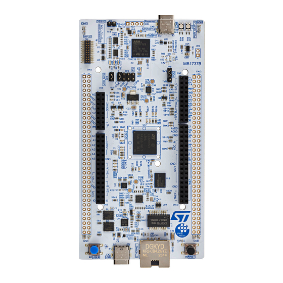
Figure 1.
NUCLEO-H7S3L8 top view
Figure 2.
NUCLEO-H7S3L8 bottom view
Pictures are not contractual.
UM3276 - Rev 1 - February 2024
www.st.com
For further information contact your local STMicroelectronics sales office.
Advertisement
Table of Contents

Related Manuals for ST NUCLEO-H7S3L8


Summary of Contents for ST NUCLEO-H7S3L8
-
Page 1: Figure 1. Nucleo-H7S3L8 Top View
STM32H7Rx/7Sx Nucleo-144 board (MB1737) Introduction The STM32H7Rx/7Sx Nucleo-144 board based on the MB1737 reference board (order code NUCLEO-H7S3L8) provides an affordable and flexible way for users to try out new concepts and build prototypes by choosing from the various combinations of performance and power consumption features, provided by the STM32H7S3L8H6 microcontroller. -
Page 2: Features
® – ST Zio expansion connector including ARDUINO Uno V3 – ST morpho extension pin headers for full access to all STM32 I/Os • Flexible power-supply options: ST-LINK USB V , USB connector, or external sources • On-board STLINK-V3EC debugger/programmer with USB re-enumeration capability: mass storage, Virtual COM port, and debug port •... -
Page 3: Ordering Information
The meaning of the codification is explained in Table Table 2. Codification explanation NUCLEO-XXYYZT Description Example: NUCLEO-H7S3L8 MCU series in STM32 32-bit Arm Cortex MCUs STM32H7 series MCU product line in the series STM32H7R3/7S3 includes the STM32H7S3L8 MCU STM32 package pin count: 225 pins •... -
Page 4: Development Environment
STM32 flash memory for easy demonstration of the device peripherals in standalone mode. The latest versions of the demonstration source code and associated documentation can be downloaded from www.st.com. UM3276 - Rev 1 page 4/40... -
Page 5: Conventions
UM3276 Conventions Conventions Table 3 provides the conventions used for the ON and OFF settings in the present document. Table 3. ON/OFF convention Convention Definition Jumper JPx ON Jumper fitted Jumper JPx OFF Jumper not fitted Jumper JPx [1-2] Jumper fitted between Pin 1 and Pin 2 Solder bridge SBx ON SBx connections closed by 0 Ω... -
Page 6: Quick Start
Table Table 4. Default jumper configuration Jumper Definition Default position Comment External debugger selection Debug with internal ST-LINK IDD measurement VDD_MCU current measurement 5 V power source selection (user USB power source [1-2] 5V source from STLINK-V3EC selection) VDD voltage selection [1-2] The VDD voltage selection is 3V3. -
Page 7: Figure 3. Default Board Configuration
UM3276 Quick start Figure 3. Default board configuration JP1 OFF JP3 [1-2] JP5 [1-2] JP2 ON UM3276 - Rev 1 page 7/40... -
Page 8: Table 5. Jumper Configuration
Table 5. Jumper configuration Jumper Definition Setting Comment Debug with internal ST-LINK External debugger selection Debug with an external debugger MCU is powered by the on-board power supplies. Use an ammeter to measure the MCU power consumption, or connect an... -
Page 9: Hardware Layout And Configuration
TFBGA225 package. Figure 4 shows the connections between the STM32 and its peripherals (STLINK-V3EC, flash memory, push- button, LEDs, USB, ST Zio expansion connectors, and ST morpho headers). Figure 5 shows the location of these features on the STM32H7Rx/7Sx Nucleo-144 board. -
Page 10: Pcb Layout
Power status LED (LD9) MIPI20 (CN1) 5V Power sources (JP3) Green/yellow/red user 3.3 V/1.8 V LEDs (LD1/LD2/LD3) VDD selection (JP5) VDD_MCU (JP2) ST Zio connector ST Zio connector supporting supporting ® ® ARDUINO Uno V3 ARDUINO Uno V3 (CN8/CN9) (CN7/CN10) -
Page 11: Mechanical Drawing
UM3276 Hardware layout and configuration Mechanical drawing Figure 6. STM32H7Rx/7Sx Nucleo-144 board mechanical drawing (in millimeters) UM3276 - Rev 1 page 11/40... -
Page 12: Embedded Stlink-V3Ec
STLINK-V3EC product (for example to add new functionalities, fix bugs, and support new microcontroller families), it is recommended to keep the STLINK-V3EC firmware up to date before starting to use the NUCLEO-H7S3L8 board. The latest version of this firmware is available from the www.st.com website. -
Page 13: Using An External Debug Tool To Program And Debug The On-Board Stm32
UM3276 Hardware layout and configuration 6.3.3 Using an external debug tool to program and debug the on-board STM32 The STM32H7Rx/7Sx Nucleo-144 board supports an external debug tool CN1 for SWD/JTAG and trace debugging. Keep the embedded STLINK-V3EC running. Power on the STLINK-V3EC at first until the COM LED turns red. -
Page 14: Power Supply And Power Selection
The STLINK-V3EC MCU (U14) determines the maximum current. The NUCLEO-H7S3L8 Nucleo board with its shield can be powered from the STLINK-V3EC USB connector (CN5), but only the STLINK-V3EC circuit has the power before USB enumeration because the host PC only provides 100 mA to the board at that time. -
Page 15: Figure 7. Jp3 [1-2]: 5V_Stlk Power Source
UM3276 Hardware layout and configuration 5V_STLK configuration: The JP3 jumper is set on [1-2] as shown in Figure Figure 7. JP3 [1-2]: 5V_STLK power source STLINK-V3EC ® USB Type-C (CN5) Green LED (LD5) JP3 [1-2] UM3276 - Rev 1 page 15/40... -
Page 16: Figure 8. Jp3 [3-4]: 5V_Vin Power Source
VIN (5VIN) is the 7 to 12 V DC power from the ARDUINO the connector silkscreen or from the ST morpho connector (CN11) pin 24. The JP3 jumper must be on pin [3-4] to select the 5V_VIN power source. In this case, the DC power comes from the power supply through the ®... -
Page 17: Figure 9. Jp3 [5-6]: 5V_Ext Power Source
5V_EXT 5V_EXT is the DC power coming from an external 5 V DC power from the ST morpho connector (CN11) pin 6. In this case, the JP3 jumper must be set on [5-6] to select the EXT power source. The green LED (LD5) is turned... -
Page 18: Figure 10. Jp3 [7-8]: 5V_Ucpd Power Source
UM3276 Hardware layout and configuration 5V_UCPD ® 5V_UCPD is the DC power supply connected to the USB Type-C user connector (CN2) when it is used as a sink port. In this case, the JP3 jumper must be set on [7-8] to select the UCPD power source. The green LED (LD5) is turned ON. -
Page 19: Programming/Debugging When The Power Supply Is Not From Stlink-V3Ec (Stlk)
3. Power on the external power supply. 4. Check that the 5 V green LED (LD5) is turned ON. 5. Connect the PC to the USB ST-LINK connector (CN5). If this sequence is not respected, the V from STLINK-V3EC might power the board first, and the following risks might be encountered: •... -
Page 20: Vdd_Mcu Idd Measurement
The user green LED (LD1) is connected to the PD10 STM32 I/O (SB50 ON and SB49 OFF, default configuration) or PA5 (SB50 OFF and SB49 ON, optional configuration corresponding to the D13 ST Zio expansion connector). A transistor is used to drive the LED whatever the MCU 1V8 or 3V3 voltage range is. -
Page 21: Push-Buttons
UM3276 Hardware layout and configuration Tricolor PWR status LED (LD9) The tricolor (green, orange, and red) LED (LD9) provides information about the STLINK-V3EC target power status. • LED OFF: The target is not powered by STLINK-V3EC. • Green: The Nucleo board power request is less or equal to the USB port power capability. •... -
Page 22: Osc Clock Supply
SB14 and SB15 OFF. The external crystal is not connected to HSE. • SB66 and SB67 ON. The ST morpho pins are connected as GPIOs. Reset sources The reset signal of the Nucleo board is active LOW and the reset sources include: •... -
Page 23: Bootloader
6.10 Bootloader The bootloader is located in the system memory, programmed by ST during production. It is used to reprogram the flash memory via USART, I C, SPI, CAN FD, or USB FS in device mode through the device firmware upgrade (DFU). -
Page 24: Ethernet
RMII interface. Table 10 describes the pinout of the Ethernet function. Table 10. Ethernet pinout Configuration when using Configuration when using ST Zio or ST STM32 pin Signal name Ethernet morpho connector RMII reference clock SB63 ON... -
Page 25: Expansion Connectors
® • Zio connectors (CN7, CN8, CN9, and CN10) supporting ARDUINO Uno V3 • ST morpho expansion connectors (CN11 and CN12). ® Zio connectors supporting ARDUINO Uno V3 ® The Zio connectors (CN7, CN8, CN9, and CN10) are female connectors supporting the ARDUINO ®... -
Page 26: Table 11. Arduino ® -Included Zio Connector (Cn7) Pinout
UM3276 Expansion connectors ® The related pinout for the Zio connectors supporting ARDUINO Uno V3 is listed in Table Table Table Table ® ‑included Zio connector (CN7) pinout Table 11. ARDUINO STM32 STM32 MCU function Signal name Pin number Signal name MCU function name name... -
Page 27: Table 14. Arduino ® -Included Zio Connector (Cn10) Pinout
UM3276 Expansion connectors STM32 STM32 MCU function Signal name Pin number Signal name MCU function name name ADC12_IN8 USART_B_CTS USART2 I2C1 I2C_A_SDA ADC1_IN2 PF11 I2C1 I2C_A_SCL COMP1 SAI_A_MCLK SAI1_A COMP2 SAI_A_FS SAI1_A I2C2 I2C_B_SMBA SAI_A_SCK SAI1_A I2C2 I2C_B_SCL SAI_A_SD SAI1_A I2C2 I2C_B_SDA SAI_B_SD... -
Page 28: St Morpho Headers (Cn7 And Cn10)
ST morpho headers (CN7 and CN10) The ST morpho consists of CN11 and CN12 male pin header footprints (not soldered by default). They can be used to connect the STM32 Nucleo-144 board to an extension board or a prototype/wrapping board placed on top of the STM32 Nucleo-144 board. -
Page 29: Table 15. St Morpho Connector Pin Assignment
UM3276 Expansion connectors Table 15 shows the pin assignments for the STM32 on the ST morpho connector. Table 15. ST morpho connector pin assignment CN7 odd pins CN7 even pins CN10 odd pins CN10 even pins Pin number Pin name... -
Page 30: Solder Bridge Configuration For The Expansion Connector
PC8 is connected to ST morpho CN12 pin 2 and Zio CN8 pin 2: SDMMC_D0 signal quality can be impacted. SB38 PC8 is not connected to ST morpho CN12 pin 2 to avoid stub on Zio CN8 SDMMC_D0. SDMMC IO PC8/PC9 PC9 is connected to ST morpho CN12 pin 1 and Zio CN8 pin 4. - Page 31 ST morpho CN12 pin 17: Ethernet signal RMII REF CLK quality can be impacted. SB52 PB6 is not connected to ST morpho CN12 pin 17 to avoid stub on Ethernet. 1. The default configuration is in bold. UM3276 - Rev 1...
-
Page 32: Nucleo-H7S3L8 Product Information
B01. The second line shows the board serial number used for traceability. Parts marked as “ES” or “E” are not yet qualified and therefore not approved for use in production. ST is not responsible for any consequences resulting from such use. In no event will ST be liable for the customer using any of these engineering samples in production. -
Page 33: Nucleo-H7S3L8 Product History
UM3276 NUCLEO-H7S3L8 product information NUCLEO-H7S3L8 product history Table 17. Product history Order Product Product details Product change description Product limitations code identification MCU: • STM32H7S3L8H6 silicon revision "Y" MCU errata sheet: NUH7S3L8$KR1 Initial revision No limitation • STM32H7Rxx/Sxx device errata (ES0596) Board: •... -
Page 34: Federal Communications Commission (Fcc) And Ised Canada Compliance
UM3276 Federal Communications Commission (FCC) and ISED Canada Compliance Statements Federal Communications Commission (FCC) and ISED Canada Compliance Statements FCC Compliance Statement Part 15.19 This device complies with Part 15 of the FCC Rules. Operation is subject to the following two conditions: (1) this device may not cause harmful interference, and (2) this device must accept any interference received, including interference that may cause undesired operation. -
Page 35: Revision History
UM3276 Revision history Table 19. Document revision history Date Revision Changes 08-Feb-2024 Initial release. UM3276 - Rev 1 page 35/40... -
Page 36: Table Of Contents
UM3276 Contents Contents Features................2 Ordering information . - Page 37 NUCLEO-H7S3L8 product information ........
-
Page 38: List Of Tables
ST morpho connector pin assignment........ -
Page 39: List Of Figures
ST morpho connectors (CN7 and CN10) ........ - Page 40 ST’s terms and conditions of sale in place at the time of order acknowledgment. Purchasers are solely responsible for the choice, selection, and use of ST products and ST assumes no liability for application assistance or the design of purchasers’...
Need help?
Do you have a question about the NUCLEO-H7S3L8 and is the answer not in the manual?
Questions and answers