Table of Contents
Advertisement
Quick Links
UM3301
User manual
STM32WBA Nucleo-64 board (MB1801 and MB1803)
Introduction
NUCLEO-WBA55CG
is a wireless and ultra-low-power board embedding a powerful and ultra‑low‑power radio compliant with
®
®
the Bluetooth
Low Energy SIG specification v5.4, IEEE 802.15.4-2015 PHY and MAC, supporting Thread
, Matter, and
®
Zigbee
.
®
The ARDUINO
Uno V3 connectivity support and the ST morpho headers allow the easy expansion of the functionality of the
STM32 Nucleo open development platform with a wide choice of specialized shields.
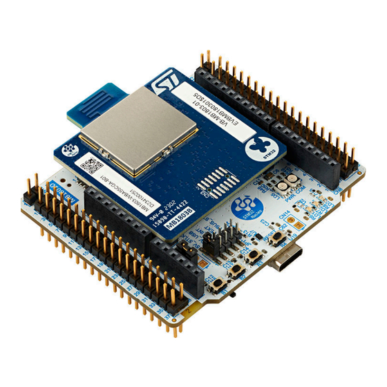
Figure 1.
NUCLEO-WBA55CG global view
Picture is not contractual.
UM3301 - Rev 2 - June 2024
www.st.com
For further information contact your local STMicroelectronics sales office.
Advertisement
Table of Contents

Subscribe to Our Youtube Channel
Related Manuals for ST MB1801


Summary of Contents for ST MB1801
-
Page 1: Figure 1. Nucleo-Wba55Cg Global View
® Zigbee ® The ARDUINO Uno V3 connectivity support and the ST morpho headers allow the easy expansion of the functionality of the STM32 Nucleo open development platform with a wide choice of specialized shields. Figure 1. NUCLEO-WBA55CG global view Picture is not contractual. -
Page 2: Features
USB Type-C ® ◦ ARDUINO Uno V3 expansion connector ◦ ST morpho headers for full access to all STM32 I/Os • Flexible power-supply options: ST-LINK USB V or external sources • On-board STLINK-V3EC debugger/programmer with USB re-enumeration capability: mass storage, Virtual COM port, and debug port •... -
Page 3: Ordering Information
1. Additional information is available from the datasheet and reference manual of the target microcontroller. Table 1. List of available products Order code Board reference Target STM32 • MB1801 NUCLEO-WBA55CG STM32WBA55CG • MB1803 1. Mezzanine board 2. MCU RF board Codification... -
Page 4: Development Environment
STM32 flash memory for easy demonstration of the device peripherals in standalone mode. The latest versions of the demonstration source code and associated documentation can be downloaded from www.st.com. UM3301 - Rev 2 page 4/45... -
Page 5: Conventions
UM3301 Conventions Conventions Table 3 provides the conventions used for the ON and OFF settings in the present document. Table 3. ON/OFF convention Convention Definition Jumper JPx ON Jumper fitted Jumper JPx OFF Jumper not fitted Jumper JPx [1-2] Jumper fitted between Pin 1 and Pin 2 Solder bridge SBx ON SBx connections closed by 0 Ω... -
Page 6: Safety Recommendations
UM3301 Safety recommendations Safety recommendations Targeted audience This product targets users with at least basic electronics or embedded software development knowledge like engineers, technicians, or students. This board is not a toy and is not suited for use by children. Handling the board This product contains a bare printed circuit board and as with all products of this type, the user must be careful about the following points:... -
Page 7: Quick Start
STLINK-V3MODS and STLINK-V3MINI debugger/programmer tiny probes for STM32 microcontrollers (UM2502) available at www.st.com. 5. Use the ST BLE Toolbox mobile application to detect the STM32WBA P2P server (P2PSRV) and connect it. The smartphone application displays the service and characteristics of the device. -
Page 8: Hardware Layout And Configuration
Figure 2 illustrates the connection between STM32WBA55CG ® and peripherals (ARDUINO Uno V3 connectors, ST morpho connector, and embedded ST-LINK). Figure 3 Figure 5 help users locate these features on the NUCLEO-WBA55CG board. The mechanical dimensions of the STM32WBA55CG product are shown in Figure Figure 2. -
Page 9: Figure 3. Nucleo-Wba55Cg Pcb Top View
Digital 0-7 (CN8) ® User push-buttons (B1, B2, and B3) User LEDs (LD1, LD2, and LD3) Reset push-button (B4) ST-LINK status LED (LD4) Figure 4. NUCLEO-WBA55CG PCB details of the MCU RF board PCB antenna C12/L1/C13/L2/C14 Matching network and filter... -
Page 10: Figure 5. Nucleo-Wba55Cg Pcb Bottom View
Figure 5. NUCLEO-WBA55CG PCB bottom view LDO 5V (U3) LDO 3V3 (U4) Level shifters (U6, U9, and U15) STM32F723 (core of ST-LINK) Power switch (U10) LDO 3V3 (U11) ® ST-LINK USB Type-C connector Figure 6. NUCLEO-WBA55CG (MB1801D) mechanical dimensions (in millimeters) -
Page 11: Figure 7. Nucleo-Wba55Cg (Mb1803B) Mechanical Dimensions (In Millimeters)
UM3301 Hardware layout and configuration Figure 7. NUCLEO-WBA55CG (MB1803B) mechanical dimensions (in millimeters) UM3301 - Rev 2 page 11/45... -
Page 12: Power Supply
® ARDUINO shield, which can deliver this type of voltage on the VIN pin • Pin VIN of the ST morpho connector (CN3-24). It is possible to apply until +12 V on this pin like for the ® ARDUINO connection •... -
Page 13: Power Supply
Section 7.1.2: 7 to 12 V power supply. • USB ST-LINK can supply the board directly (VBUS_STLK) or through the monitoring of STLINK-V3EC. The jumper (JP1) allows selecting the 5V source. Table 4 shows the configuration to apply the selected source. - Page 14 Hardware layout and configuration Jumper/solder bridge Setting Configuration 5V sources NUCLEO-WBA55CG is supplied through CN10 or through pin 6 of the ST morpho connector (CN3). Refer to the configuration details in the present Power supply section. 5V supply source selector...
-
Page 15: Current Measurement
SB1 must be ON. Figure 9 shows the configuration. Figure 9. Current measurement with an ammeter AVDDEXT (CN11-1) ARDUINO® AVDD (CN6-8) VDDA/VREF+ ST morpho AVDD (CN4-7) ARDUINO® VIN (CN5-8) JP1 [5-6] LDO 5V ST morpho VIN (CN3-24) STM32WBA55CG SB20 VEXT (CN10-1) -
Page 16: Figure 10. Current Measurement With An External Power Supply
3V3. AVDD input (CN1-8) must not be used during this measurement. Figure 10. Current measurement with an external power supply AVDDEXT (CN11-1) ARDUINO® AVDD (CN6-8) VDDA/VREF+ ST morpho AVDD (CN4-7) ARDUINO® VIN (CN5-8) JP1 [5-6] LDO 5V ST morpho VIN (CN3-24) STM32WBA55CG... -
Page 17: Figure 11. Current Measurement With Stlink-V3Pwr
The height of ® the connector is not compatible with the plug of the ARDUINO shield. Moreover, it is always possible to plug an ST morpho shield on the bottom side of MB1801. UM3301 - Rev 2 page 17/45... -
Page 18: Table 5. Components To Add To Support The Stlink-V3Pwr Configuration
UM3301 Hardware layout and configuration Figure 12. CN3 assembly for STLINK-V3PWR It is also necessary to add some components on the bottom side of MB1803. Table 5 explains the values of the components and Figure 13 shows the location of these components. Table 5. -
Page 19: Figure 14. Configuration For Current Measurement With Stlink-V3Pwr
With this configuration, the second Virtual COM port (VCP2) is not available from STLINK-V3PWR. Only VCP1 can be used. VCP1 is directly connected by the STDC14 ribbon (pins 13 and 14 on STDC14). After connection, download STM32CubeMonitor-Power from the www.st.com website and install it. This software allows doing easily dynamic current measurements. -
Page 20: Clock Sources
® www.st.com. For Windows 10 , it is not necessary to install the driver. ST-LINK is automatically identified. In case the NUCLEO-WBA55CG board is connected to the PC before the driver is installed, some board interfaces might be declared as Unknown in the PC device manager. In this case, the user must install the dedicated driver files and update the driver of the connected device from the device manager, as shown in Figure 16. -
Page 21: Stlink-V3Ec Firmware Upgrade
VCP1 of the STLINK-V3EC MCU (STM32F723IE). Access is possible on the CN3 connector of the mezzanine board (MB1801). Both signals Tx and Rx are available, and two solder bridges, SB3 and SB5, allow disconnecting the UART coming from the SoC. By default, VCP1 is connected to the USART1 of NUCLEO-WBA55CG. -
Page 22: Virtual Com Port Lpuart1 (Vcp2)
It is possible to replace the mass storage interface with a second Virtual COM port. To do so, the two solder bridges SB7 and SB8 (Tx and Rx on MB1801) must be ON. It is also necessary to do a firmware upgrade through STM32CubeProgrammer (refer to the technical note Overview of ST-LINK derivatives (TN1235) at www.st.com. -
Page 23: Leds
LD5: This LED gives information about the STLINK-V3EC target power. • LD6: This LED blinks during communication with the PC. For detailed information about the STLINK-V3EC LEDs, refer to the technical note Overview of ST-LINK derivatives (TN1235) at www.st.com. Table 9. -
Page 24: Push-Buttons
UM3301 Hardware layout and configuration Push-buttons 7.6.1 Description NUCLEO-WBA55CG provides two types of buttons: • USER1 push-button (B1) • USER2 push-button (B2) • USER2 push-button (B3) • Reset push-button (B4), used to reset the Nucleo board. Figure 18. Push-button location User push-button (B1) User push-button (B2) User push-button (B3) -
Page 25: Rf I/O Stage
This antenna is described in the application note Guidelines for meander design using low-cost PCB antennae with 2.4 GHz radio for STM32WB/WB0 MCUs (AN5129) available at www.st.com. Between the STM32WBA55CG and the antenna, there is a passive network. This network has two functions: makes a low pass filter and matches the impedance of the PCB antenna. -
Page 26: Connector Naming
Connector location and naming MCU RF board connector MCU RF board connector (CN2) (CN1) ARDUINO connector ® ARDUINO connector ® (CN6) (CN5) ST morpho connector ST morpho connector (CN4) MB1803 (CN3) ARDUINO connector ® ARDUINO connector ® (CN8) (CN7) MB1801 ®... -
Page 27: Figure 22. Arduino ® Connector Pinout
UM3301 Hardware layout and configuration ® Figure 20 shows the position of the ARDUINO shield when it is plugged into NUCLEO-WBA55CG. The pinout ® shown in Figure 22 corresponds to standard ARDUINO naming. To see the correspondence with the STM32, refer to Table ®... -
Page 28: Table 12. Pinout Of The Arduino ® Connectors
UM3301 Hardware layout and configuration ® Table 12. Pinout of the ARDUINO connectors Connector Pin number Signal name STM32 port Comment NC (reserved for tests) 3V3 (IOREF) IOREF 3V3 NRST NRST NRST External supply input (+12 V) ADC1_IN2 ADC1_IN3 ADC1_IN7 ADC1_IN8 PA5/PA8 ADC1_IN4/ADC1_IN1... -
Page 29: St Morpho Interface And Pinout
ST morpho interface and pinout The ST morpho connectors (CN3 and CN4) are male pin headers accessible on both sides of the board. All signals and power pins of the MCU are available on the ST morpho connectors. An oscilloscope, logical analyzer, or voltmeter can also probe these connectors. -
Page 30: Table 13. St Morpho Connector Pinout
PB9/PC13 PA11 PC14 /PB15 PC15 PB14 OSC_IN PA11 OSC_OUT VBAT PC13 PA5/PA8 PB12 PA0/PA5 PA10 1. Optional, need to change the state of solder bridges. 2. Not available on NUCLEO-WBA55CG (MB1801-NoUSB mezzanine board variant) UM3301 - Rev 2 page 30/45... -
Page 31: Mcu Rf Board Interface And Pinout
Hardware layout and configuration 7.11 MCU RF board interface and pinout The ST-MCU RF board connectors (CN1 and CN2) are accessible on the top side of the board. They are used to plug the MCU RF board into the mezzanine board. Figure 24. -
Page 32: Mipi10/Stdc14 Connector
By default, on this footprint (CN3), the connector is not assembled. If some features are not available on STLINK- V3EC embedded on the MB1801, it is possible to solder a MIPI10 or STDC14 connector. This enables the use of an external debugger. Nevertheless, it is necessary to disconnect the SWD (SB15 and SB17 OFF on the MB1801). -
Page 33: Table 15. Pinout Of The Mipi10/Stdc14 Connector (Cn3 Of The Mcu Rf Board)
UM3301 Hardware layout and configuration This description uses the standard name of the MIPI10 and STDC14 connectors. On the NUCLEO-WBA55CG T_VCP corresponding to T_VCP1 on STDC14 (T_VCP_TX is T_VCP1_TX and T_VCP_RX is T_VCP1_RX). Figure 25. Pinout of the MIPI10/STDC14 connector (CN3 of the MCU RF board) STDC14 MIPI10 Table 15. -
Page 34: Nucleo-Wba55Cg Product Information
B01. The second line shows the board serial number used for traceability. Parts marked as “ES” or “E” are not yet qualified and therefore not approved for use in production. ST is not responsible for any consequences resulting from such use. In no event will ST be liable for the customer using any of these engineering samples in production. -
Page 35: Nucleo-Wba55Cg Product History
MCU: STM32WBA55CGU6 silicon revision "B" MCU errata sheet: STM32WBA5x device errata (ES0592) NUWBA55CG$DT1 Initial revision No limitation Boards: • MB1801-NoUSB-D02 (mezzanine board) • MB1803-WBA55CGA- (MCU RF board) Board revision history Table 17. Board revision history Board reference Board variant and revision... -
Page 36: Federal Communications Commission (Fcc) And Ised Canada Compliance
UM3301 Federal Communications Commission (FCC) and ISED Canada Compliance Statements Federal Communications Commission (FCC) and ISED Canada Compliance Statements FCC Compliance Statement Identification of products: NUCLEO-WBA55CG Contains FCC ID: YCP-MB180300 Part 15.19 This device complies with Part 15 of the FCC Rules. Operation is subject to the following two conditions: (1) this device may not cause harmful interference, and (2) this device must accept any interference received, including interference that may cause undesired operation. -
Page 37: Ised Compliance Statement
UM3301 Federal Communications Commission (FCC) and ISED Canada Compliance Statements ISED Compliance Statement Identification of products: NUCLEO-WBA55CG Contains IC ID: 8976A-MB180300 Identification du produit : NUCLEO-WBA55CG Contient sous-ensemble certifié IC : 8976A-MB180300 Compliance Statement Notice: This device complies with ISED Canada licence-exempt RSS standard(s). Operation is subject to the following two conditions: (1) this device may not cause interference, and (2) this device must accept any interference, including interference that may cause undesired operation of the device. -
Page 38: Red Compliance Statement
Hereby, STMicroelectronics declares that the radio equipment type "NUCLEO-WBA55CG" is in compliance with Directive 2014/53/EU. The full text of the EU declaration of conformity is available at the following internet address: www.st.com. Déclaration de conformité UE simplifiée STMicroelectronics déclare que l'équipement radioélectrique du type "NUCLEO-WBA55CG" est conforme à la directive 2014/53/UE. -
Page 39: Ukca Compliance Statement
Hereby, the manufacturer STMicroelectronics, declares that the radio equipment type “NUCLEO-WBA55CG” is in compliance with the UK Radio Equipment Regulations 2017 (UK S.I. 2017 No. 1206). The full text of the UK Declaration of Conformity is available at the following internet address: www.st.com. UM3301 - Rev 2... -
Page 40: Revision History
UM3301 Revision history Table 18. Document revision history Date Revision Changes 02-Apr-2024 Initial release. Updated document title, Features, Hardware block diagram, NUCLEO- ® WBA55CG PCB details of the MCU RF board, and ARDUINO connector pinout figures, and Pinout of the MIPI10/STDC14 connector (CN3 of the MCU 04-Jun-2024 RF board) table. -
Page 41: Table Of Contents
UM3301 Contents Contents Features................2 Ordering information . - Page 42 ST morpho interface and pinout ........
-
Page 43: List Of Tables
ST morpho connector pinout ........ -
Page 44: List Of Figures
ST morpho connector pinout ........ - Page 45 ST’s terms and conditions of sale in place at the time of order acknowledgment. Purchasers are solely responsible for the choice, selection, and use of ST products and ST assumes no liability for application assistance or the design of purchasers’...
Need help?
Do you have a question about the MB1801 and is the answer not in the manual?
Questions and answers