Table of Contents
Advertisement
Quick Links
Evaluating the LTC3303A, 3.3 V to 1.2 V at 4 A, 2 MHz Synchronous Step-Down Regulator in a 2 mm × 2 mm SWF FCQFN
FEATURES
LTC3303A
evaluation board
►
Transient circuit included for load-transient evaluation
►
EMI filter included to reduce noise in EMI emission tests
►
EVALUATION KIT CONTENTS
DC3252A evaluation board
►
DOCUMENTS NEEDED
LTC3303A data sheet
►
EQUIPMENT NEEDED
One 5 V, 4 A, DC power supply
►
One 4 A, Electronic load
►
Three digital voltmeters
►
Two digital ammeters
►
GENERAL DESCRIPTION
Demonstration Circuit DC3252A features the LTC3303A, 5 V, 4 A
synchronous step-down silent switcher operating as a 2 MHz, 3.3
V to 1.2 V, 4 A buck regulator. The LTC3303A supports adjustable
output voltages from 0.5 V to V
high efficiency, and high-speed synchronous monolithic step-down
switching regulator. A minimum on-time of 27 ns enables high V
low V
conversion.
OUT
The DC3252A operating mode can be selected as Burst Mode
operation, skip (PS) or forced continuous (FC) mode. Setting JP1
to the SKIP position allows the LTC3303A to sync to a clock
frequency from 1.6 MHz to 2.4 MHz. The LTC3303A operates in
forced continuous mode when syncing to an external clock.
The DC3252A also has an EMI filter to reduce conducted EMI. This
EMI filter can be included by applying the input voltage at the V
EMI terminal. The EMI performance of the board is shown in the
EMI Test Results
section. The red lines in the EMI performance
graphs show the CISPR25 Class 5 peak limits for the conducted
and radiated emission tests.
PLEASE SEE THE LAST PAGE FOR AN IMPORTANT
WARNING AND LEGAL TERMS AND CONDITIONS.
Arrow.com.
Downloaded from
. The LTC3303A is a compact,
IN
User Guide | DC3252A
The LTC3303A data sheet gives a complete description of the
device, operation, and application information. Full specifications on
the LTC3303A are available in the LTC3303A data sheet available
from Analog Devices, Inc., and must be consulted with this user
guide when using the DC3252A evaluation board. The LTC3303A is
assembled in a 2 mm × 2 mm FCQFN package with side wettable
flanks (SWF) for visual solder inspection. The layout recommenda-
tions for low EMI operation and maximum thermal performance are
available in the data sheet section Low EMI PCB Layout.
Figure 7
shows the efficiency and the power loss of the circuit with
a 3.3 V input in Burst Mode operation.
to
IN
IN
UG-2106
Rev. 0 | 1 of 13
Advertisement
Table of Contents

Related Manuals for Analog Devices LTC3303A


Summary of Contents for Analog Devices LTC3303A
-
Page 1: Features
User Guide | DC3252A UG-2106 Evaluating the LTC3303A, 3.3 V to 1.2 V at 4 A, 2 MHz Synchronous Step-Down Regulator in a 2 mm × 2 mm SWF FCQFN The LTC3303A data sheet gives a complete description of the FEATURES device, operation, and application information. -
Page 2: Table Of Contents
Evaluation Board Hardware.........10 Documents Needed..........1 Introduction to the DC3252A......10 Equipment Needed..........1 Accurately Measuring Output Ripple of the General Description..........1 LTC3303A............10 DC3252A Evaluation Board Photograph....3 Evaluation Board Schematic........11 Performance Summary..........4 Ordering Information..........12 Quick Start Procedure........... 5 Bill of Materials..........12 Typical Performance Characteristics..... -
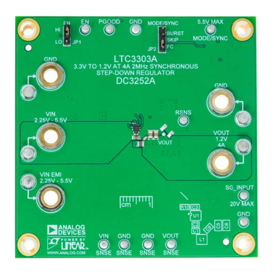
Page 3: Dc3252A Evaluation Board Photograph
User Guide DC3252A DC3252A EVALUATION BOARD PHOTOGRAPH Figure 1. DC3252A Evaluation Board Photograph analog.com Rev. 0 | 3 of 13 Arrow.com. Downloaded from... -
Page 4: Performance Summary
SWITCHING FREQUENCY > V TOP SWITCH MINIMUM ON-TIME TOP SWITCH DUTY CYCLE With 1% resistors. Accuracy improves to within 1% using 0.1% FB resistors or a fixed voltage version of the LTC3303A. analog.com Rev. 0 | 4 of 13 Arrow.com. -
Page 5: Quick Start Procedure
Demonstration circuit DC3252A is easy to set up and use to evalu- 11. If forced continuous or Burst Mode is required, set PS1 to 0 ate the performance of the LTC3303A. For the proper measurement V. Move JP1 to FC or BURST. Repeat steps 3 through 9. In... - Page 6 User Guide DC3252A QUICK START PROCEDURE Figure 2. DC3252A Simplified Schematic Figure 3. Test Setup for the DC3252A Demo Board Figure 4. Technique for Measuring Output Ripple and Step Response with a Scope Probe analog.com Rev. 0 | 6 of 13 Arrow.com.
- Page 7 User Guide DC3252A QUICK START PROCEDURE Figure 5. Technique for Measuring Output Ripple and Step Response with a Low Inductance Connector (Not Supplied) Figure 6. Optional Transient Response Circuit analog.com Rev. 0 | 7 of 13 Arrow.com. Downloaded from...
-
Page 8: Typical Performance Characteristics
User Guide DC3252A TYPICAL PERFORMANCE CHARACTERISTICS Figure 9. Load Transient Response Forced Continuous Mode Figure 7. Efficiency and Power Loss in Burst Mode Operation Figure 8. Buck Load Regulation analog.com Rev. 0 | 8 of 13 Arrow.com. Downloaded from... -
Page 9: Emi Test Results
User Guide DC3252A EMI TEST RESULTS Figure 10. Conducted EMI Performance (CISPR25 Conducted Emission Test Figure 12. Radiated EMI Performance (CISPR25 Radiated Emission Test with with Class 5 Peak Limits) Class 5 Peak Limits, Vertical) Figure 11. Radiated EMI Performance (CISPR25 Radiated Emission Test with Class 5 Peak Limits, Horizontal) analog.com Rev. -
Page 10: Evaluation Board Hardware
Current in the inductor then increases until the top switch comparator trips and turns off the top power switch. If the EN pin is low, the LTC3303A is in shutdown and in a low quiescent current state. When the EN pin is above its threshold, the switching regulator is enabled. -
Page 11: Evaluation Board Schematic
User Guide DC3252A EVALUATION BOARD SCHEMATIC Figure 15. DC3252A Schematic Diagram analog.com Rev. 0 | 11 of 13 Arrow.com. Downloaded from... -
Page 12: Ordering Information
Resistor, 20 kΩ, 1%, 1/16 W, 0402, AEC- Vishay, CRCW040220K0FKED Q200 Resistor, 10 Ω, 5%, 1/20 W, 0201 Vishay, CRCW020110R0JNED IC, 5 V, 4 A, 2 MHz, synchronous step- Analog Devices Inc., down regulator LTC3303ARUCM#TRPBF Additional Demo Board Circuit Components C7, C8 Capacitors, option, 0805... - Page 13 Evaluation Board until you have read and agreed to the Agreement. Your use of the Evaluation Board shall signify your acceptance of the Agreement. This Agreement is made by and between you (“Customer”) and Analog Devices, Inc. (“ADI”), with its principal place of business at Subject to the terms and conditions of the Agreement, ADI hereby grants to Customer a free, limited, personal, temporary, non-exclusive, non-sublicensable, non-transferable license to use the Evaluation Board FOR EVALUATION PURPOSES ONLY.
Need help?
Do you have a question about the LTC3303A and is the answer not in the manual?
Questions and answers