Table of Contents
Advertisement
Quick Links
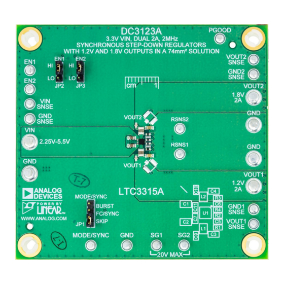
DESCRIPTION
Demonstration Circuit DC3123A features the
dual 5V, 2A Synchronous Step-Down DC/DC regulators
operating at 2MHz. One regulator provides a 1.2V output
and the other provides 1.8V, both up to a 2A load. The
LTC3315A supports adjustable output voltages from 0.5V
to V
, operating frequencies from 1MHz up to 3MHz. The
IN
LTC3315A is a compact, high efficiency, and high speed
synchronous monolithic step-down switching regulator.
Fast minimum on-time of 25ns enables high V
V
conversion at high frequency.
OUT
The DC3123A operating mode may be selected as Burst
Mode operation, Skip mode or Forced Continuous (FC)
mode. Setting JP1 to the FC/SYNC position will allow
PERFORMANCE SUMMARY
PARAMETER
Input Supply Range (V
)
IN
Internal Oscillator Frequency (f
SW
Top Switch On Time
V
OUT1
V
OUT2
V
IN
2.25V TO 5.5V
10µF
1µF
10µF
1µF
0.1µF
3.3V V
, Dual 2A, 2MHz Buck Regulators at
IN
1.2V and 1.8V Outputs in a 74mm
LTC©3315A
IN
Specifications are at T
CONDITIONS
)
0 to 2A
0 to 2A
680nH
V
SW1
IN
FB1
V
IN
LTC3315A
1µH
V
IN
SW2
FB2
EN1
EN2
MODE/SYNC
1M
PGOOD
GND
f
= 2MHz
dc3123a F01
SW
DEMO MANUAL DC3123A
the LTC3315A to sync to a clock frequency from 1MHz
to 3MHz. The LTC3315A operates in Forced Continuous
mode when syncing to an external clock.
The LTC3315A data sheet gives a complete description
of the device, operation and application information. The
data sheet must be read in conjunction with this demo.
The LTC3315A is assembled in a 1.6mm × 1.6mm WLCSP
package.
to low
The Efficiency vs Load graph shows the efficiency and
the power loss of the circuit with a 3.3V input in Burst
Mode operation.
Design files for this circuit board are
All registered trademarks and trademarks are the property of their respective owners.
= 25°C
A
V
OUT1
1.2V, 2A
3.3pF
140k
22µF
100k
V
OUT2
1.8V, 2A
3.3pF
261k
22µF
100k
V
IN
LTC3315A
2
Solution
available.
MIN
TYP
MAX
2.25
5.5
1.9
2.0
2.1
25
1.2
1.8
Efficiency vs Load Current Burst
Mode Operation
95
90
85
80
75
70
0.001
0.01
0.1
I
(A)
OUT
UNITS
V
MHz
ns
V
V
V
= 3.3V
IN
1.2 V
OUT
1.8 V
OUT
1
3
dc3123a TA01b
Rev. 0
1
Advertisement
Table of Contents

Related Manuals for Analog Devices LTC3315A


Summary of Contents for Analog Devices LTC3315A
- Page 1 DESCRIPTION Demonstration Circuit DC3123A features the LTC©3315A the LTC3315A to sync to a clock frequency from 1MHz dual 5V, 2A Synchronous Step-Down DC/DC regulators to 3MHz. The LTC3315A operates in Forced Continuous operating at 2MHz. One regulator provides a 1.2V output mode when syncing to an external clock.
-
Page 2: Board Photo
DEMO MANUAL DC3123A BOARD PHOTO BOARD PERFORMANCE LTC3315A Load Regulation LTC3315A Load Regulation 1.205 1.805 = 3.3V = 3.3V 1.204 1.804 = 1.2V = 1.8V OUT1 OUT2 FORCED CONTINUOUS MODE FORCED CONTINUOUS MODE 1.203 1.803 1.202 1.802 1.201 1.801 1.200 1.800... - Page 3 DEMO MANUAL DC3123A BOARD PERFORMANCE 1.2V Load Transient Response Forced Continuous Mode 2V/DIV RSNS1 50mV/DIV OUT1 50mV/DIV dc3123a G03 10µs/DIV 3.3V TO 1.2V LOADSTEP 0.4A TO 1.6A 1A/µs 1.8V Load Transient Response Forced Continuous Mode 2V/DIV RSNS2 50mV/DIV 50mV/DIV dc3132a G04 10µs/DIV 3.3V TO 1.8V LOADSTEP 0.4A TO 1.6A 1A/µs...
- Page 4 Observe load transient effect on V OUTx 7. Set LOAD1 to 500mA. 18. Refer to the LTC3315A data sheet for more details on 8. With power off, connect a second 0A to 2A load to how the LTC3315A operates. and GND with a series ammeter and a voltmeter OUT2 19.
-
Page 5: Quick Start Procedure
DEMO MANUAL DC3123A QUICK START PROCEDURE Figure 1. Proper Measurement Equipment Setup Figure 2. Measuring Input or Output Ripple Rev. 0... -
Page 6: Theory Of Operation
If the EN pin is Select an operating switching frequency below f SWMAX low, the LTC3315A is in shutdown and in a low quiescent The LTC3315A has a requirement that the magnitude of current state. When the EN pin is above its threshold, the the ripple current in the output inductor be greater than switching regulator will be enabled. - Page 7 DEMO MANUAL DC3123A THEORY OF OPERATION oscilloscope channel terminated to 50Ω at the scope. This The high frequency spikes are partially attributed to the will help to reduce the noise coupling onto and displaying interwinding capacitance of the inductor and the voltage on the scope.
-
Page 8: Parts List
VISHAY, CRCW0402100KFKED RES., 261k OHMS, 1%, 1/16W, 0402, AEC-Q200 VISHAY, CRCW0402261KFKED IC, DUAL 5V, 2A SYNCHRONOUS STEP-DOWN DC/DCs IN 1.6mm x ANALOG DEVICES, 1.6mm WLCSP LTC3315AECBZ-R7#PBF Additional Demo Board Circuit Components CAP ., 220uF , TANT. POSCAP , 6.3V, 20%, 7343, 18mOHMS, TPE... -
Page 9: Schematic Diagram
Devices for its use, nor for any infringements of patents or other rights of third parties that may result from its use. Specifications subject to change without notice. No license is granted by implication or otherwise under any patent or patent rights of Analog Devices. - Page 10 Board until you have read and agreed to the Agreement. Your use of the Evaluation Board shall signify your acceptance of the Agreement. This Agreement is made by and between you (“Customer”) and Analog Devices, Inc. (“ADI”), with its principal place of business at One Technology Way, Norwood, MA 02062, USA. Subject to the terms and conditions of the Agreement, ADI hereby grants to Customer a free, limited, personal, temporary, non-exclusive, non-sublicensable, non-transferable license to use the Evaluation Board FOR EVALUATION PURPOSES ONLY.
Need help?
Do you have a question about the LTC3315A and is the answer not in the manual?
Questions and answers