Table of Contents
Advertisement
Quick Links
DESCRIPTION
Demonstration circuit 2609A features the LTC6952, an
Ultralow Jitter, 4.5GHz PLL with 11 Outputs and JESD204B
Support.
By default, the DC2609A is powered from two supplies.
The 9V-12V supply input powers the onboard reference
and VCO circuitry, along with the LTC6952 5V supply pin.
The 4V-6V supply input powers the LTC6952 3.3V supply
pins. A reduced power option is provided that allows the
LTC6952's output supply pins to connect to an LTC Silent
Switcher
and the LTC6952 input supply pins to connect
®
to a low noise LDO.
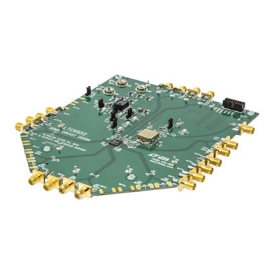
All differential inputs and six of the differential outputs are
populated with 0.5" spaced SMA connectors. These outputs
are AC-coupled with 50Ω transmission lines making them
suitable to drive 50Ω impedance instruments. The remain-
ing five differential outputs are terminated with 100Ω.
9-12V SUPPLY ,
BANANA JACK J30
4-6V SUPPLY,
BANANA JACK J32
POWER SUPPLY
SUPPORT CIRCUITRY
(TOP & BOTTOM SIDE)
STAT LED, D1
OUT9, CML
AC-COUPLED
OUTPUTS, SMA
OUT8, CML
AC-COUPLED
OUTPUTS, SMA
OUT5, CML
AC-COUPLED
OUTPUTS, SMA
Ultralow Jitter, 4.5GHz PLL with 11 Outputs
LTC6952
DEMO CIRCUIT 2609A
Figure 1. DC2609A Connections
DEMO MANUAL DC2609A
and JESD204B Support
The LTC6952's EZSync™ and SYSREF request func-
tions are made available via the LTC6952 SPI interface
or the EZS_SRQ SMA/turret connectors. The DC2609A,
DC2610A, and DC2611A SMA placement was designed
for ease of connection for all multi-part synchronization
and SYSREF request modes.
The V
and VCO SMAs can mate directly with the
TUNE
DC2664A VCO rider board. This options allows for a quick
method to evaluate multiple VCOs.
A DC2026 USB serial controller board is used for SPI
communication with the LTC6952, controlled by the sup-
plied LTC6952Wizard™ software.
DC2609 Design files are available.
All registered trademarks and trademarks are the property of their respective owners.
RIBBON CABLE CONNECTION
TO DC590 OR DC2026
ONBOARD REFERENCE
(BOTTOM SIDE)
ONBOARD VCO &
SUPPORT CIRCUITRY
OUT0, CML
AC-COUPLED
OUTPUTS, SMA
OUT1, CML
AC-COUPLED
OUTPUTS, SMA
OUT4, CML
AC-COUPLED
OUTPUTS, SMA
LTC6952
Rev 0
1
Advertisement
Table of Contents

Subscribe to Our Youtube Channel
Related Manuals for Analog Devices LTC6952


Summary of Contents for Analog Devices LTC6952
- Page 1 The 9V-12V supply input powers the onboard reference and SYSREF request modes. and VCO circuitry, along with the LTC6952 5V supply pin. The 4V-6V supply input powers the LTC6952 3.3V supply The V...
- Page 2 The LTC6952Wizard software is used to communi- The LTC6952Wizard and the DC2026 are required to con- cate with the LTC6952. It uses the DC2026 to translate trol the DC2609A through a personal computer (PC). between USB and SPI-compatible serial communications formats.
-
Page 3: Quick Start Procedure
Microsoft.NET and install the LTC6952Wizard. The DC2609A’s red STAT LED (D1) should illuminate. Refer to the LTC6952Wizard Help menu for software 5. Synchronize outputs by toggling the LTC6952 SSYNC operation. bit on then off from the LTC6952Wizard. 6. Connect desired output (OUT9, OUT8, OUT5, OUT4,... -
Page 4: Troubleshooting
1. Verify J32 measures between 4V and 6V (see the Typi- using Linduino. cal DC2609A Requirements and Characteristics) If DC2609A performance is less than the LTC6952 2. Verify JP4, JP6, and JP7 jumpers are installed correctly data sheet specifications: (refer to the DC2609A schematic sheet 3) 1. -
Page 5: Dc2609A Reconfiguration
Table 3 to identify the required DC2609A powers the higher current LTC6952 output supply pins board modifications. Refer to the LTC6952 data sheet for from an LTC Silent Switcher, such as the LT8609S. The SYNC timing and level requirements. -
Page 6: Frequently Asked Questions
Yes, follow these steps. Step 1: Configure the DC2026 for 3.3V SPI as shown in Figure 2 Step 2: Connect the DC2026 J1 connector SPI pins to the LTC6952 SPI pins. Refer to page two of the DC2609A sche- matic for pin assignments. -
Page 7: Typical Dc2609A Requirements And Characteristics
JP3 to position 2-3. 4V-6V Power Supply Input J32 Banana Jack Powers the LTC6952 3.3V supply pins (V , and V ). Option available to power supplies from single LDO, or an LDO and an LTC Silent Switcher. Refer to Table 1. -
Page 8: Parts List
DEMO MANUAL DC2609A PARTS LIST ITEM REFERENCE PART DESCRIPTION MANUFACTURER/PART NUMBER Required Circuit Components CI1_A, C3, CP_A (OPT) CAP ., OPTION, 0603 CI1_P CAP ., 0.68µF, X7R, 16V, 10%, 0603, AEC- SAMSUNG, CL10B684KO8VPNC Q200 CI2_A (OPT) CAP ., OPTION, 1206 CI2_P CAP ., 1µF, X7R, 25V, 10%, 1206, AEC-Q200 SAMSUNG, CL31B105KAPWPNE CP_P... - Page 9 DEMO MANUAL DC2609A PARTS LIST ITEM REFERENCE PART DESCRIPTION MANUFACTURER/PART NUMBER FB4, FB5 IND., 220Ω at 100MHz, FERRITE BEAD, 3A, TDK, MPZ2012S221AT000 0.04Ω, 0805 JP1, JP2, JP3, JP4, JP5, JP6, JP7 CONN., HDR, MALE, 1 × 3, 2mm, THT, STR Wurth Elektronik, 62000311121 J1, J2, J7, J8, J13, J14, J15, J16, CONN., SMA, JACK, RCPT, END LAUNCH,...
-
Page 10: Schematic Diagram
Note: The buffers shown on sheet 2 of 4 of the schematic are used to protect the LTC6952 when connected to the DC2026 before the LTC6952 is powered up. There is no need for such circuitry if the SPI bus is not active before powering up the LTC6952. The EEPROM is for identification and is not needed to program the LTC6952. - Page 11 DEMO MANUAL DC2609A SCHEMATIC DIAGRAM Rev 0...
- Page 12 DEMO MANUAL DC2609A SCHEMATIC DIAGRAM Rev 0...
- Page 13 DEMO MANUAL DC2609A SCHEMATIC DIAGRAM Rev 0...
- Page 14 DEMO MANUAL DC2609A SCHEMATIC DIAGRAM Rev 0...
-
Page 15: Layout Top Layer
Devices for its use, nor for any infringements of patents or other rights of third parties that may result from its use. Specifications subject to change without notice. No license is granted by implication or otherwise under any patent or patent rights of Analog Devices. - Page 16 Board until you have read and agreed to the Agreement. Your use of the Evaluation Board shall signify your acceptance of the Agreement. This Agreement is made by and between you (“Customer”) and Analog Devices, Inc. (“ADI”), with its principal place of business at One Technology Way, Norwood, MA 02062, USA. Subject to the terms and conditions of the Agreement, ADI hereby grants to Customer a free, limited, personal, temporary, non-exclusive, non-sublicensable, non-transferable license to use the Evaluation Board FOR EVALUATION PURPOSES ONLY.
Need help?
Do you have a question about the LTC6952 and is the answer not in the manual?
Questions and answers