Table of Contents
Advertisement
Quick Links
RC32508A
Evaluation Board
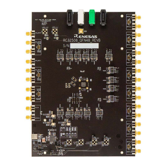
The RC32508A evaluation board (EVB) is designed
to help users evaluate the RC32508A Clock
Generator, also known as FemtoClock 2x2. The
RC32508A supports jitter attenuator and synthesizer
functionality.
When the evaluation board (EVB) is connected via
USB to a computer running the Renesas RICBox™
Software, FemtoClock 2x2 can be configured and
programmed to generate frequencies with best-in-
class performance. FemtoClock 2x2 has eight output
pairs that can be programmed to CMOS, LVDS, or
HCSL style outputs.
R31UH0024EU0100 Rev.1.00
Aug 11, 2023
Features
■
Develop configurations with Renesas RICBox
software and upload to the EVB through USB
■
Can be powered from the USB connection
■
EVB is a combination evaluation with Renesas
Low Noise power supply regulators
■
Clock input and output pairs are DC coupled
Board Contents
■
Renesas RC32508A ultra-low noise synthesizer
and jitter attenuator
■
Renesas RAA214020 low-noise power supply
regulators
■
FTDI FT232HQ USB-to-I2C bridge
Figure 1. RC32508A Board
Evaluation Board Manual
© 2023 Renesas Electronics
Page 1
Advertisement
Table of Contents

Related Manuals for Renesas RC32508A


Summary of Contents for Renesas RC32508A
-
Page 1: Figure 1. Rc32508A Board
Evaluation Board Manual RC32508A Evaluation Board Features The RC32508A evaluation board (EVB) is designed to help users evaluate the RC32508A Clock ■ Develop configurations with Renesas RICBox Generator, also known as FemtoClock 2x2. The software and upload to the EVB through USB RC32508A supports jitter attenuator and synthesizer ■... -
Page 2: Table Of Contents
Figure 18. RC32508A EVB – Block Diagram ....................... 12 Figure 19. RC32508A Board – Top View ......................13 Figure 20. RC32508A Evaluation Board Schematics – Page 1 ................15 Figure 21. RC32508A Evaluation Board Schematics – Page 2 ................16 Figure 22. -
Page 3: Functional Description
The board can fully function with just the USB cable to a computer. Renesas’ RICBox Software is used to control the RC32508A on the board. RICBox is compatible with both the on-board USB-to-I2C bridge and the Aardvark adapter. RICBox uses a software wizard for entering the overall configuration and has several tools to fine tune the configuration (for example, block diagram GUI). -
Page 4: Figure 3. Create New Project Window
RC32508A Evaluation Board Manual Figure 3. Create New Project Window 5. From the Select Product Family section, select the device family that is being used. From the Select a Product Variant section, select the working device. Click the OK button to open the new configuration. -
Page 5: Board Power Supply
RC32508A Evaluation Board Manual Board Power Supply The power source for each V pin can be selected with jumpers. The voltage for each pin, except two pins, is 1.8V. The exception is VDDD-0 and VDDD-1, which can be powered with 1.8V or 3.3V. -
Page 6: Differential Outputs
RC32508A Evaluation Board Manual Differential Outputs The right side of the board has eight SMA pairs for the eight differential outputs. See Figure 7 for an SMA pair example. Figure 7. Differential Output Pair Example The board is shipped with the SMA connectors DC coupled to the RC32508 output pins. Output pairs can be programmed to LVDS, HCSL or CMOS logic. -
Page 7: Differential Inputs
The SMA connector XIN_REF0 AC couples to the pin XIN/REF-0 and the SMA connector XIN_REF1 AC couples to the pin XIN/REF-1 of the RC32508A device. A clock can be used to overdrive XIN. When deciding to use an actual crystal for XIN/REF-0 / XOUT-0, ensure to remove the AC coupling capacitor assembled at R10 to disconnect the PCB trace to J25. -
Page 8: Setup And Configuration
RC32508A Evaluation Board Manual Setup and Configuration Complete the following steps to start the configuration of the board. 1. When creating a new configuration, the wizard page is the first screen to appear (see Figure 10). The wizard contains a pull-down list of configuration pages (located in the upper right-hand corner of the window) pertaining to different sections of the device that require overall configuring. -
Page 9: Figure 11. Jitter Attenuator Mode Settings Window
RC32508A Evaluation Board Manual Figure 11. Jitter Attenuator Mode Settings Window 3. The Output Clocks window (screen 3 of 3) sets up the outputs (see Figure 12). a. Fill in the desired output frequencies. Leave blank unused outputs. b. Click on Advanced Settings at the red arrow to select Logic Type and Signal Amplitude. -
Page 10: Figure 12. Output Settings Window
RC32508A Evaluation Board Manual Figure 12. Output Settings Window Figure 13. Block Diagram R31UH0024EU0100 Rev.1.00 Page 10 Aug 11, 2023... -
Page 11: Figure 14. Side Panel Buttons
RC32508A Evaluation Board Manual 4. The side panel consists of five separate buttons. The buttons on the top left are Control Panel (the above screen), Wizard, Configuration, Registers, and Block Diagram. For more information, see the Renesas IC Toolbox (RICBox) Software Manual. -
Page 12: Board Design
USB port from most of the supply current. The board has an FTDI USB-to-I2C bridge for programming FemtoClock 2x2 from a computer. Renesas RICBox software is available for easy development of configurations. -
Page 13: Figure 19. Rc32508A Board - Top View
RC32508A Evaluation Board Manual Figure 19. RC32508A Board – Top View R31UH0024EU0100 Rev.1.00 Page 13 Aug 11, 2023... - Page 14 RC32508A Evaluation Board Manual Table 1. RC32508A – EVB Pins and Functions Note: See Figure 19 for reference numbers in the following table. Ref. Name On-Board Connector Label Function Output0_0 J65, J66 Differential Clock Output 0-0 Output0_1 J63, J64 Differential Clock Output 0-1...
-
Page 15: Schematic Diagrams
Jack for external VEE connection For factory testing only. Is connected to GND by default. GND Jack Jack for external Power Supply Ground Schematic Diagrams Figure 20. RC32508A Evaluation Board Schematics – Page 1 R31UH0024EU0100 Rev.1.00 Page 15 Aug 11, 2023... -
Page 16: Figure 21. Rc32508A Evaluation Board Schematics
RC32508A Evaluation Board Manual Figure 21. RC32508A Evaluation Board Schematics – Page 2 R31UH0024EU0100 Rev.1.00 Page 16 Aug 11, 2023... -
Page 17: Figure 22. Rc32508A Evaluation Board Schematics
RC32508A Evaluation Board Manual Figure 22. RC32508A Evaluation Board Schematics – Page 3 R31UH0024EU0100 Rev.1.00 Page 17 Aug 11, 2023... -
Page 18: Ordering Information
RC32508A Evaluation Board Manual 3. Ordering Information Part Number Description RC32508A-EVK RC32508A Evaluation Board; A-male to USB-C cable. 4. Revision History Revision Date Description 1.00 Aug 11, 2023 Initial release. R31UH0024EU0100 Rev.1.00 Page 18 Aug 11, 2023... - Page 19 Renesas' products are provided only subject to Renesas' Terms and Conditions of Sale or other applicable terms agreed to in writing. No use of any Renesas resources expands or otherwise alters any applicable warranties or warranty disclaimers for these products.
- Page 20 Mouser Electronics Authorized Distributor Click to View Pricing, Inventory, Delivery & Lifecycle Information: Renesas Electronics RC32508A-EVK...
Need help?
Do you have a question about the RC32508A and is the answer not in the manual?
Questions and answers