Table of Contents
Advertisement
Quick Links
Advertisement
Table of Contents

Related Manuals for KStar YDC3300 Series


Summary of Contents for KStar YDC3300 Series
- Page 1 YDC3300 Maintenance manual Shenzhen Kstar Science & Technology Co.,Ltd...
-
Page 2: Table Of Contents
Contents Contents ............................. I FigureContents ......................... III Table contents .......................... IV Product introduction ......................1 Summary ......................1 Appearance ......................1 Features ......................2 Operating panel ....................2 System block diagram ......................4 block diagram ..................... 4 AC/DC & DC/DC principle circuit diagram ............4 Inverter DC/AC principle .................. - Page 3 5.10 USB interface board ..................32 5.11 parallel interface board ..................33 Inspection before installation..................34 Room environment inspection ................. 34 UPS location inspection ..................34 UPS visual inspection ..................34 External cables and switch capacity inspection..........34 External auto switching and generator power distribution inspection.... 35 Battery inspection ....................
-
Page 4: Figurecontents
Appendix A UPS fault judgment ..................65 FigureContents Figure 1 Appearance ......................... 2 Figure 2. Operating interface ....................3 Figure 3 block diagram ......................4 Figure 4 AC/DC & DC/DC principle .................... 5 Figure 5 Bypass and inverter principle ..................5 Figure 6. - Page 5 Figure 48 Inverter power board....................28 Figure 49 DSP board ........................ 29 Figure 50. adapter interface ....................31 Figure 51.RJ45 interface board interface ................31 Figure 52.EPO interface board interface ................. 32 Figure 53 .USB interface board interface ................33 Figure 54.parallel interface board interface ................
-
Page 6: Product Introduction
1. Product introduction 1.1 Summary YDC3300 Series is a kind of high-frequency online intelligent UPS and adopts double DSP control chips, advanced control technology and double conversion topology. It eliminates various interference of the grid and makes the output a stable and pure sine wave power with low noise, no interference and low distortion. -
Page 7: Features
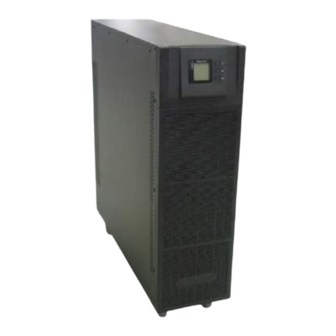
Figure 1 Appearance 1.3 Features ◆ Three-phase in to three-phase out UPS This series is three-phase in to three-phase out UPS with large capacity, the input current of three phase is balanced which can balance the load of each phase. ◆... - Page 8 Cycle button Status indicator 1. error alarm OFF button 2. bypass 3.battery 4. mains input ON button LCD display Figure 2. Operating interface Status indicator on front panel, LCD and other buttons LCD and indicator LED on front panel, cooperate with buttons, can view all the data, information and set parameters.
-
Page 9: System Block Diagram
System block diagram 2.1 block diagram Bps switch AC/DC DC/AC mains DC/DC output Output switch Battery fuse battery CHARGER fuse Figure 3 block diagram As shown above, there is a bypass switch. When switch on it, the power will go to the bypass road. -
Page 10: Inverter Dc/Ac Principle
Figure 4 AC/DC & DC/DC principle As shown above, A (yellow box) shows the rectifier circuit, B (blue box) shows the battery input circuit, C (other part) shows the boost circuit. A and C form the PFC rectifier circuit while B and C form the battery boost circuit. -
Page 11: Charging Principle
As shown above, A (yellow box) represents bypass circuit of UPS, B (blue box) shows the inverter circuit, which converts the Bus voltage into the AC output. 2.4 Charging principle battery Charging fuse Figure 6. Charging principle As shown above, charger reduces the Bus voltage to a suitable voltage to charge the battery. - Page 12 Power Factor 0.9/1.0 Voltage Regulation ±1% synchronize with input; when input frequency >±10% (± Utility 1%/±2%/±4%/±5% optional), Mode output (50/60±0.1%)Hz. Frequency Battery (50/60±0.1%)Hz Mode Crest Factor ≤2% with linear load ≤5% with non linear load ≥93.5% at ≥94.5% at normal mode Efficiency normal mode...
-
Page 13: Internal Structure
Altitude < 1500m.When>1500m,lower the rated power for use Standard unit:250×900×868 Unit Dimensions(W×D×H) Other Long run unit:250×580×655 Weight (Kg) 129/35 186/39 187/40 236/43 239/46 Safety Conformance IEC/EN62040-1,IEC/EN60950-1 IEC/EN62040-2,IEC61000-4-2,IEC61000-4-3,IEC61000-4-4,IEC61 000-4-5,IEC61000-4-6,IEC61000-4-8 4 Internal structure 4.1 The whole appearance Button Company LOGO Figure 7. UPS front view... - Page 14 Output Switch RS232 port REPO port Maintenance switch RS485 port Intelligent Slot 1 USB port (SNMP card) Intelligent Slot 2 Dry contact card (SNMP card) Parallel port 2 Input breaker Parallel port 1 Baffle for terminal block Figure 8. UPS rear view (10-20K)
- Page 15 Output Switch RS232 port REPO port Maintenance switch RS485 port Intelligent Slot 1 USB port (SNMP card) Dry contact port Intelligent Slot 2 (SNMP card) Parallel port 2 Input Switch Parallel port 1 Terminal block Figure 9. UPS rear view (30-40K) Terminal block Figure 10.
-
Page 16: Internal View Of Ups
Terminal block Figure 11. Terminal block (30-40K) 4.2 Internal view of UPS LCD display board PFC power board Control detection board INV. Power board Battery EMI board ( ) Figure 12.UPS left view... - Page 17 PFC inductor board INV inductor board Input/Output EMI board ( ) Figure 13.UPS right view LCD display board PFC power board Control detection board INV. Power board Battery EMI board ( ) Figure 14.UPS left view 15-20KVA...
- Page 18 PFC inductor board INV inductor board Input/Output EMI board ( ) Figure 15.UPS right view 15-20KVA LCD display board PFC power board Control detection board INV. Power board Battery EMI board Battery fuse ( ) Figure 16.UPS left view 30KVA...
- Page 19 PFC driver board PFC inductor board INV inductor board Input/Output EMI board ( ) Figure17.UPS right view 30KVA LCD display board PFC power board Control detection board INV. Power board Battery fuse Battery EMI board ( ) Figure18.UPS left view 40KVA...
- Page 20 PFC driver board PFC inductor board INV inductor board Input/Output EMI board ( ) Figure19.UPS right view 40KVA Battery fuse 6pcs PFC inductors 2pcs charging inductors ( ) Figure20.PFC inductor board 6pcs PFC inductors Battery fuse 2pcs charging inductors ( )...
- Page 21 6pcs PFC inductors 2pcs charging inductors ( ) Figure22.PFC inductor board 30-40K Radiator Charging fuse IGBT drive board ( ) Figure23.PFC power board Radiator Charging fuse IGBT drive board ( ) Figure24.PFC power board 15-20K Radiator Charging fuse IGBT drive board (...
- Page 22 BUS capacitor 6pcs inv. inductors 3pcs inv. capacitors Figure17. Inverter inductor board (10K) BUS capacitor 6pcs inv. inductors 3pcs inverter fuse 6pcs inv. capacitors Figure18. Inverter inductor board (15-20K) BUS capacitor 6pcs inv. inductors 3pcs inverter fuse 3pcs inv. capacitors Figure19.
- Page 23 BUS capacitor 6pcs inv. inductors 3pcs inverter fuse 3pcs inv. capacitors Figure20. Inverter inductor board (40K) Auxiliary power Radiator Figure 1. INV. Power board Figure 2. Control detection board Figure 3. Battery EMI board...
- Page 24 Figure 4. EMI board (10-20K) Figure 5. EMI board (30-40K) Figure 6.PFC drive board Figure 7. Adapter...
-
Page 25: Pcb Boards And Their Signals
Figure 8.RJ45 interface board Figure 9.EPO interface board Figure 10.USB interface board Figure 11. parallel interface board 5 PCB boards and their signals 5.1 PFC inductor board Function overview Mains rectifier Battery input circuit... - Page 26 Bypass static switch Boost inductor circuit Charging inductor circuit Figure 12. PFC inductor board Input and output interface definition Table 4 PFC inductor board interface Definition Specification Name Description Name: Copper connection Battery fuse lock BAT+ Description: HPM3350-RM Copper 1 red copper T2 BAT+ terminal T=1.5mm Fog tin...
-
Page 27: Pfc Drive Board
Definition Specification Name Description PIN white Name:neilsbed Neutral Description:4PIN 60A M4 threaded straight foot copper Neutral mist tin plating Name:neilsbed Main A phase input Description:4PIN 60A M4 threaded straight foot copper Main A phase input mist tin plating Name:neilsbed Main B phase input Description:4PIN 60A M4 threaded straight foot copper Main B phase input mist tin plating 9.2*11.1*10.5mm... - Page 28 Figure 13.PFC drive board interface Input and output interface definition Table 5 PFC drive board interface description Definition Specification Name Description Name:neilsbed PFC drive board PFC drive board signal Description:1121S-6P P=3.96mm 180 degree single row signal square PIN white Name:neilsbed positive charger SCR positive charger Description:2001R-1*2P 2PIN P=2.54mm 90 °...
-
Page 29: Pfc Power Board
Definition Specification Name Description drive3 Description: 1121R-1*2P 2PIN P=3.96mm 90 degree single SCR drive3 row PIN yellow Name:neilsbed A phase bypass SCR1 A phase bypass Description: 1121R-1*2P 2PIN P=3.96mm 90 degree single BPS_A_SCR1 drive SCR1 drive row PIN yellow Name:neilsbed A phase bypass SCR2 A phase bypass Description:... -
Page 30: Inv. Inductor Board
Definition Specification Name Description BUS+ Name:blade terminal Description:4PIN 10A M4 screw hole straight leg BUS+ BUS+ T=0.8mm BUS- Name:blade terminal Description:4PIN 10A M4 screw hole straight leg BUS- BUS- T=0.8mm 301S-2*15P 30PIN P=2.54mm 180° two rows square PIN PFC/charger drive PFC/charger drive signal black horn signal... - Page 31 Figure 16 Inv. Inductor board (15-20K) Figure 17 Inv. Inductor board (30K) Figure 18 Inv. Inductor board (40K) Input and output interface definition Table 7 Inv. Inductor board interface Definition Specification Name Description...
- Page 32 Definition Specification Name Description VOUT_A Name:blade terminal Output A phase Description:4PIN 10A M4screw hole straight leg VOUT_A Output A phase T0.8mm tinned copper BPS_A Name:blade terminal Bypass A phase Bypass A phase Description:4PIN 10A M4screw hole straight leg T0.8mm BPS_A Output Output tinned copper...
-
Page 33: Inverter Power Board
Definition Specification Name Description B phase inv.DC square PIN white Output voltage component and Output sampling voltage sampling PH3_INV_Q_C1E2&VO C phase inv.DC UT_C Name:neilsbed PH3_INV_Q_C1 component and C phase inv.DC Description:1121S-1*3P 3PIN P=3.96mm 180° single row E2&VOUT_C Output voltage component and Output square PIN white sampling voltage sampling... -
Page 34: Dsp Board
Definition Specification Name Description REC temperature Description:2001S-2P P=2.54mm 180 degree single row _SWITCH detection detection square PIN white Name:neilsbed upper half bridge INV upper half bridge Description:301S-2*6P 12PIN P=2.54mm 180 ° 2PIN Black drive signal INV drive signal horn ASSISTANT Name:neilsbed ASSISTANT POWER... - Page 35 Definition Specification Name Description A phase INV A phase INV Name:neilsbed voltage/output voltage/output voltage Vinv_A/Vout_A Description:Hip3340-RM M17.PCB HPM3340 voltage sampling sampling signal signal B phase INV B phase INV Name:neilsbed voltage/output voltage/output voltage Vinv_B/Vout_B Description:Hip3340-RM M17.PCB HPM3340 voltage sampling sampling signal signal C phase INV C phase INV...
-
Page 36: Adapter Board
Definition Specification Name Description drive signal Description:301S-2*6P 12PIN P=2.54mm 180° two rows drive signal square PIN black horn Name:neilsbed lower half bridge INV lower half bridge Description:301S-2*5P 10PIN P=2.54mm 180° two rows drive signal drive signal square PIN black horn 5.7 Adapter board Function overview:... -
Page 37: Epo Interface Board
Input and output interface definition Table 11 RJ45 interface board interface Definition Specification Name Description Name:neilsbed RJ45_2 signal Description:2001R-1*5P 5PIN P=2.54mm 90 degree single RJ45_2 RJ45_2 signal row square PIN beige Name:neilsbed RJ45_1 signal Description:2001R-1*5P 5PIN P=2.54mm 90 degree single RJ45_1 RJ45_1 signal row square PIN beige... -
Page 38: Parallel Interface Board
Figure 24 .USB interface board interface Input and output interface definition Table 13 USB interface board interface Definition Specification Name Description Name:neilsbed RS232(USB) signal Description:2001S-1*4P 4PIN P=2.54mm 180 degrees EPO signal single row PIN white Name:neilsbed Dry contact Dry contact signal Dry Contact Description:2001S-1*4P 4PIN P=2.54mm 180 degrees signal... -
Page 39: Inspection Before Installation
Definition Specification Name Description Name:PC interface Parallel Parallel signal2 Parallel signal2 Description:DB15 Male Seat P=2.29mm Black 90 ° signal2 Screw Separate with Serial Port 6 Inspection before installation 6.1 Room environment inspection UPS room: UPS should be installed in a cool, dry, clean and well-ventilated environment, such as the room temperature should be <... -
Page 40: External Auto Switching And Generator Power Distribution Inspection
For power cable selection and connection method, please refer to the user manual and related specification. Check if the breakers rated capacity of UPS input, Output and distribution cabinet are appropriate. Pay attention to the Neutral and Ground protection inspection: If the Neutral and Ground cable size meets the requirement? Neutral has separate input and output, connect to the same Neutral is not allowed. -
Page 41: Ups Maintenance
deal it according to the local regulations. If the electrolyte touches your skin, immediately wash it with a plenty of water. 10) The battery must be handled with reference to local environmental regulations. Focus on the following aspects: If the battery surface is clean, the appearance is damaged, deformed and leakage; Check if the connection among battery is reliable, if the screws are tightened, if there is corrosion and confirm that all battery terminals are coated with insulating material;... -
Page 42: Security Conditions
7.2 Security conditions Warning: When the UPS is operating, all the electronic parts connected directly to the power supply and all internal components including the battery exist high voltage. Even disconnected from the power supply, all internal parts including the battery still have dangerous voltage (except the communication output) . -
Page 43: Troubleshooting
3.1Please refer to the user’s manual on UPS installation content; 3.2 First read chapter 2 “Security conditions” 3.3 If the UPS is in need of repair, the process A operation is recommended(This is completely safe) : Disconnect all input power supply and battery. Load is allowed to turn off for process A. - Page 44 : Warning when UPS works, a large amount of energy is stored in the internal BUS capacitor, it cannot be guaranteed that there is no electricity inside the UPS with mains isolation, so it needs extra attention when maintenance. Disconnect all external input power of the fault machine for maintenance.
- Page 45 according to the “replace PCB”; 3. If fan doesn’t work with mains input, confirm that if the auxiliary power of the INV-POWER board is damaged and needs to be replaced 4. Charger shows abnormal, check if the charging circuit in the PFC power board is damaged and need to be replaced.
- Page 46 board control Inv. SCR short long INV inductor board detection beep Fault ON board control Inv. SCR break long INV inductor board detection beep Fault ON board control Bypass SCR short long PFC inductor board detection beep Fault ON board control Bypass SCR break long...
- Page 47 Rectifier PFC power board over-temperature twice/s Fault ON Inv. INV power board Over-temperature twice/s Fault ON Reserve twice/s Fault ON control Battery reverse connection wrong detection twice/s Fault ON board control Parallel connection Parallel cable not detection fault connected well twice/s Fault ON board...
-
Page 48: Battery Replacement
Redundancy control Overload in parallel once/2 output overload number setting detection INV flash is improper board Mains voltage once/2 Input voltage abnormal BATTERY ON abnormal Mains frequency once/2 Input frequency abnormal BATTERY ON abnormal Bypass ultra bypass abnormal protection BPS flash Bypass ultra tracking BPS flash bypass abnormal... -
Page 49: Pcb Replacement
5. Measure the total voltage of the battery; 6. Install all screws, baffles, switch on the battery switch (if have). 8.2 Single Battery cabinet: 1. Close the battery switch (if have) 2. Disconnect the connection between the UPS and the battery cabinet; 3. - Page 50 2. Operate according to the steps 1-3 of process A or steps 1-3 of process B in chapter 3. Remove the screws of left panel of UPS, remove the cover, use the bleeder resistor to release the energy stored in the Bus capacitor; 4.
- Page 51 3. Remove the screws of left panel of UPS, remove the cover, use the bleeder resistor to release the energy stored in the Bus capacitor; 4. Remove all the cables of the PFC power board 5. Remove all the screws of the PFC power board; 6.
-
Page 52: Replace Fan
3. Open the front panel, remove 4pcs of nuts of the rear panel and then remove the rear panel; 4. Remove all the cables of the PCB 5. Remove all the screws of the PCB; 6. Replace the PCB, package the old PCB; 7. -
Page 53: Stand-Alone Commissioning
BOOST IGBT Q1-12 E->C diode ≈0.4V open or short BOOST IGBT Q1-12 Ω ≈10KΩ open or short Charge FUSE F3-4 Ω 0Ω open Charge MOSFET Q13-14 S->D diode ≈0.46V open or short Charge MOSFET Q13-14 Ω ≈20KΩ open or short INV inductor board Description Type... -
Page 54: Shutdown Steps
Stand-alone mode Figure 21 YDC3300 settings Close the external battery breaker, check if the charge current on the LCD is normal Simulate mains power failure test: Disconnect external main input breaker and check if the UPS can transfer to battery inv. Mode and the output is uninterrupted. Then close the external mains breaker to confirm the UPS enter the line mode. - Page 55 Mode setting (Note: Inside the broken-line is the flashing part.) After entering the setting menu, its mode setting defaulted, and the mode setting line flashing as in above picture. ①Use button “” to choose different mode. There are 3 different modes for setting: ECO, PAL, NOR. ②Press “ON”...
- Page 56 When powered by inverter, it is necessary to turn off the inverter before setting voltage and frequency level. Frequency setting Frequency setting (Note: Inside the broken-line is the flashing part.) In the output voltage setting press “ON” or in battery capacity setting press “OFF”, it goes to the frequency setting.
- Page 57 In the frequency setting press “ON” or in battery quantity setting press “OFF”, it goes to the battery capacity setting. The battery capacity line flashes as in above picture. ①Use button “” to choose the different battery capacity. Battery capacity range is 1-999Ah. (Note: long-press of “”...
- Page 58 Bypass voltage lower limit setting (Note: Inside the broken-line is the flashing part.) In the bypass voltage upper limit setting press “ON” or in parallel ID setting press “OFF”, it goes to the bypass lower limit setting. The bypass lower limit line flashes as in above picture. (“-” for negative, positive does not have any symbol.) ①Use button “”...
- Page 59 state shows as the figure (Note: ON shows MUTE, OFF shows NO MUTE).①Press button “” for Mute Cycle Settings, mute choice has On and Off. ②Press button “ON” exits mute setting and save mute setting state and change to battery self-test settings. ③Press button “OFF” exits mute setting and change to bypass voltage lower limit setting.
- Page 60 Battery temperature compensation sensor switch setting (Note: the information in the red box will be flashing) Press “ON” under the periodical battery self-test setting or press “OFF” under device address setting, goes to the battery temperature compensation switch setting. The setting state flashes as above picture shows (Note: OFF means turn off the sensor switch, ON means turn on the sensor switch, send query command to sensor with address 11,12 every second.
- Page 61 device address is1~15, it is the MODBUS device address at RS232 & RS485 communication ports. ①Press “” to set the address, with options 1~15. When battery temperature sensor is open, can choose 1~10 & 13~15; If it’s parallel mode and device address <= parallel quantity, device address= parallel ID.
- Page 62 Parallel quantity setting (Note: Inside the broken-line is the flashing part.) When under the parallel ID setting press “ON” or when under parallel redundancy quantity setting press “OFF”, it goes to the parallel quantity setting. The parallel quantity flashes as in above picture. ①Use button “” to set the parallel quantity.
-
Page 63: Parallel System Commissioning
above picture. ①Use button “” to set the parallel redundancy quantity. The parallel redundancy quantity range is 0~3. ②press “ON” to exit the mode setting and save the mode setting value and then UPS LCD panel setting is accomplished. ③Press “OFF” to go to parallel quantity setting. 13 Parallel system commissioning Warning:... -
Page 64: Shutdown Steps
5) For Unit 3 and Unit 4 UPS , the operation setting are all the same as Unit 1 and 6) Turn on Bypass/input/output breaker of all the paralleled UPS , then confirm all the setting are correct. Each UPS has their owed different ID. 7) There are only one master in parallel system .The one has a dot behind parallel mode is the master. -
Page 65: Emergency Shutdown
13.3 Emergency shutdown Connect all the EPO ports to a key switch according to the following figure. When emergency occurs, switch on the key can turn off all the outputs of UPS in this parallel system. 14 Software upgrade There are two methods for software upgrade. 14.1 Use C2000 emulator to upgrade When shutdown the UPS, remove the right panel of UPS, burn the DSP in control detection... - Page 66 unsuccessful”. Switch off the UPS and then restart, click “Update” to re-burn. If it fails during the INV burning, it will show “Program was unsuccessful”. Switch off the UPS and then restart, modify the ID number to 1 in the software. Close the serial port and then open it, click “Re-Update”...
- Page 67 Figure(1) 14.2.1.5 After the above steps, it shows below Fig (2), pls click the “OK” button Figure(2) 14.2.1.6 Connect the UPS RS232 to the computer’s serial port, make sure the communication between them is good Figure(3) 14.2.1.7 After set up the communication between UPS and computer, click “Update” as...
- Page 68 shown in Figure (4) Figure(4) 14.2.1.8 Figure (5) shows the chip is preparing for the program Figure(5) 14.2.1.9 Figure (6) shows the program work is proceeding Figure(6)
- Page 69 14.2.1.10 Follow below Figs 7/8/9 to finish and exit. If need go on the programming, pls return to step 3. If finish and stop the programming, pls turn OFF the maintenance breaker, put on the panel, work the UPS to inverter power supply. Figure(7) Figure(8) Figure(9)
- Page 70 Appendix A UPS fault judgment Software judgment UPS Alarm Condition 1 Condition 2 Condition 3 Condition 4 Buzz long Rectifier fault DC BUS over-voltage DC BUS under-voltage Large bus difference beep Fault ON The absolute value of the output voltage >112.5% of rated Inv.
- Page 71 Software judgment UPS Alarm Condition 1 Condition 2 Condition 3 Condition 4 Buzz long Positive battery Charge fault beep Fault ON long Negative battery Charge fault beep Fault ON +bus voltage>470V -bus voltage>470V long Bus over-voltage Last time: 20ms Last time: 20ms beep Fault ON Bus voltage <280V...
- Page 72 Software judgment UPS Alarm Condition 1 Condition 2 Condition 3 Condition 4 Buzz Rectifier over-current once/s Fault flash Bypass over-current X phase Bypass Output current greater than the rated 125% once/s BPS flash INV or BPS Over load X phase load rate( Inv. or Bypass) greater than rated 105% once/s flash BATTERY...
- Page 73 Software judgment UPS Alarm Condition 1 Condition 2 Condition 3 Condition 4 Buzz g) battery reverse and shutdown h) user operation fault(maint. Bypass close) i) Auxiliary power power down and shutdown 2) manually start invalid Reserve Inverter not on Once per Output switch not ON seconds...
Need help?
Do you have a question about the YDC3300 Series and is the answer not in the manual?
Questions and answers