Table of Contents
Advertisement
1
Introduction
2
Related Documentation
Table 1. Related documentation
Document
LA1224 Reference Design Board
(LA1224-RDB-B) Reference
Manual
LA1224 Reference Design Board
(LA1224-RDB-B) Errata
LA1224 Product Brief
LA1224 Data Sheet
LA1224-RDB-B-GSG
LA1224 Reference Design Board Getting Started Guide
Rev. 1 — 4 August 2022
The Layerscape Access LA1224 reference design board (LA1224-RDB-B) is a
development board with a combination of NXP LX2160A CPU processor and NXP
LA1224 programmable baseband processor with 5G-NR fixed wireless access and 3GPP
infrastructure equipment.
The LA1224-RDB-B comes preloaded with a board support package (BSP) based on a
standard Linux kernel. The board is lead-free and RoHS-compliant.
The LA1224-RDB-B functions with an integrated development environment (IDE),
such as CodeWarrior Development Studio. For instructions on how to work with the
CodeWarrior Development Studio IDE, see
LS series - ARM V8 ISA, Targeting
This document supports LA1224-RDB-B board revision B. It provides details of different
board components and explains how to set up and boot the board.
Note:
This document describes usage of the LA1224-RDB-B in configurations for LA1215,
LA1225, and LA1235 products, which are defined with no support for low-speed (LS)
data conversion subsystem (DCS). LA1224 Rev. B0 silicon populated on current revision
of LA1224-RDB-B supports LS DCS.
The following table lists the additional documents that you can refer to for more
information about the LA1224-RDB-B.
Some of these documents may be available only under a non-disclosure agreement
(NDA). To request access to these documents, contact your local NXP field applications
engineer or sales representative.
Description
Provides a detailed description of the LA1224-RDB-B
Lists the details of all known LA1224-RDB-B errata and their
fixes
Provides a brief overview of the LA1224 processor
Provides information about LA1224 electrical characteristics,
hardware design considerations, and ordering information
CodeWarrior Development Studio for QorIQ
Manual.
User guide
COMPANY CONFIDENTIAL
Link / how to access
Contact NXP FAE /
sales representative
Contact NXP FAE /
sales representative
Contact NXP FAE /
sales representative
Contact NXP FAE /
sales representative
Advertisement
Table of Contents

Related Manuals for NXP Semiconductors LA1224


Summary of Contents for NXP Semiconductors LA1224
-
Page 1: Introduction
LA1224 programmable baseband processor with 5G-NR fixed wireless access and 3GPP infrastructure equipment. The LA1224-RDB-B comes preloaded with a board support package (BSP) based on a standard Linux kernel. The board is lead-free and RoHS-compliant. The LA1224-RDB-B functions with an integrated development environment (IDE), such as CodeWarrior Development Studio. -
Page 2: Hardware Kit Contents
(usually JTAG) while connected to a developer workstation through Ethernet or USB Hardware kit contents The table below lists the items included in the LA1224-RDB-B hardware kit. Table 2. Hardware kit contents Item description Quantity... -
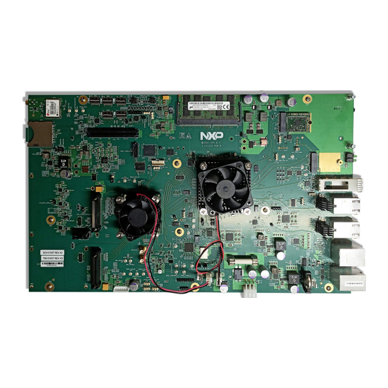
Page 3: Board Pictures
LA1224-RDB-B-GSG NXP Semiconductors LA1224 Reference Design Board Getting Started Guide Board pictures The figure below shows the top-side of the LA1224-RDB-B board. Figure 1. LA1224-RDB-B Top-side The figures below shows the bottom-side of the LA1224-RDB-B board. Figure 2. LA1224-RDB-B bottom-side LA1224-RDB-B-GSG All information provided in this document is subject to legal disclaimers. - Page 4 LA1224-RDB-B-GSG NXP Semiconductors LA1224 Reference Design Board Getting Started Guide The following figure shows the connectors available on the top-side of the LA1224-RDB- B board. J511,J29 J527 J505 J525 JP1,J6 J526 J2 J3 J512 J537 J21,J8,J9 J516 J513 J517 J524...
- Page 5 J515 J540 J534 J517 D504 D503 J536,J535 J539 Figure 4. Jumpers, LEDs, and switches available on top-side of LA1224-RDB-B The following image shows the connectors and switches available on the bottom-side of the LA1224-RDB-B board. P500 SW500 J500 J510 J509 Figure 5. Connectors and pushbutton available on bottom-side of LA1224-RDB-B LA1224-RDB-B-GSG All information provided in this document is subject to legal disclaimers.
-
Page 6: Reset Button
LA1224-RDB-B-GSG NXP Semiconductors LA1224 Reference Design Board Getting Started Guide Reset button The LA1224-RDB-B has a reset button for manually triggering a system reset. The table below describes the reset button. Table 3. Reset button Identifier Label Function Description SW500 PORST System reset Reset switch available on chassis. - Page 7 LA1224-RDB-B-GSG NXP Semiconductors LA1224 Reference Design Board Getting Started Guide Table 4. LA1224-RDB-B connectors ...continued Connector Description Connector type Typical connection LA1224_I2C3 1x3-pin header Provides remote access to LA1224 I2C3 bus MODEM1_SYNC_OUT U.FL connector Sync out signal to MODEM1_SYNC_OUT pin of onboard...
- Page 8 LA1224-RDB-B-GSG NXP Semiconductors LA1224 Reference Design Board Getting Started Guide Table 4. LA1224-RDB-B connectors ...continued Connector Description Connector type Typical connection J517 Hirose Electric Co. Ltd 20-pin connector LS DCS plug-in card IO slot FX23-20P-0.5SV20 J518, J519 SYSCLK_MDM_125M U.FL connectors 125 MHz SYSCLK output from Si5518...
-
Page 9: Jumpers
PCIe connector to interface with LA1246-MOD card Jumpers Jumpers (or shorting headers) are used to select some options that either do not change often or involve power conduction. The LA1224-RDB-B jumpers are described in the table below. Table 5. LA1224-RDB-B jumpers Jumper... - Page 10 • Shorted: RESET_REQ_B pin triggers system reset when asserted (default setting) J506 1x2-pin header VDD_DEBUG_SDA • Open: LA1224 VDD out of PF5200 (U909) is controlled from LA1224 device (default setting) • Shorted: LA1224 VDD out of PF5200 (U909) is controlled from LX2160A device J507...
-
Page 11: Lx2160A-Specific Dip Switches
• 0: Allow write to SYSID and UEFI flash • 1: Write-protect SYSID and UEFI flash (default setting) LA1224-specific DIP switches LA1224-RDB-B has four 8-pin dual inline package (DIP) switches that are used to perform LA1224-specific power-on reset (POR) configuration settings. LA1224-RDB-B-GSG All information provided in this document is subject to legal disclaimers. - Page 12 LA1224-RDB-B-GSG NXP Semiconductors LA1224 Reference Design Board Getting Started Guide For DIP switch: • "ON" setting corresponds to 1 • "OFF" setting corresponds to 0 The table below describes LA1224-specific switch settings. Table 7. LA1224-specific switch settings Switch Supported function Settings...
- Page 13 SW6[3] SD_MUX_SEL LA1224_SD_MUX_SEL • 0: LA1224 SerDes1 eight lanes connect with LX2160A SerDes3 (default setting) • 1: LA1224 SerDes1 first four lanes connect with LX2160A SerDes3 (x4 operation) and LA1224 SerDes1 last four lanes connect with PCIex8 slot (x4 operation) SW6[4] •...
-
Page 14: Lx2160A-Specific Leds
LA1224_POR Indicates LA1224_PORESET_B is asserted to the LA1224 processor and system is the process of restart PWR_FAIL_LA12xx Indicates power failure status for LA1224 related power supplies LA1224-RDB-B-GSG All information provided in this document is subject to legal disclaimers. © NXP B.V. 2022. All rights reserved. -
Page 15: Getting Started With La1224-Rdb-B
12 Getting started with LA1224-RDB-B This section explains: • Section 12.1 • Section 12.2 12.1 Prerequisites To set up LA1224-RDB-B, you need the items listed in the table below. Table 10. Prerequisites Item Available in Purpose / required action board kit? Hardware... - Page 16 Note: To make a console connection for LX2160A device, connect the RJ45-to-DB9 female cable to the LX2160A_UART (Bottom) port (J70) on the chassis and to make a console connection for the LA1224 device, connect the RJ45-to-DB9 female cable to the LA1224_UART (Top) port (J70) on the chassis.
- Page 17 00000050: 00000000 00000000 00000000 00000000 00000060: 00000000 00000000 00027008 00000000 00000070: 09d20010 00150020 Model: NXP Layerscape LA1224-RDB Board Board: LA1224-RDB, Board version: C, boot from FlexSPI NOR DEV#0 SERDES1 Reference: Clock1 = 100MHz Clock2 = 161.13MHz SERDES2 Reference: Clock1 = 100MHz Clock2 = 100MHz...
- Page 18 After U-Boot, if you do not hit any key to stop autoboot, the prebuilt kernel image boots to Linux prompt. 11. To boot the LA1224 device and its IPs (VSPA, FreeRTOS, and so on), firmware images are required to be copied in the "/lib/firmware" path in Root File System (rootfs).
-
Page 19: Troubleshooting
(NDA). To request access to the document, contact your local field applications engineer or sales representative. 12.3 Troubleshooting This section explains the basic troubleshooting tips for the LA1224-RDB-B. 12.3.1 U-Boot log not displaying Perform the following steps in case console is not showing any print: •... -
Page 20: Revision History
LA1224-RDB-B-GSG NXP Semiconductors LA1224 Reference Design Board Getting Started Guide – SW1[7] is set correctly and POR LED is blinking, indicates some configuration problem causing LX2160 asserting RESET_REQ_B. • Software check – If U-Boot log is still not showing on console, then the BSP image available in the current XSPI serial NOR flash device may be corrupt. -
Page 21: Legal Information
NXP Semiconductors. In the event that customer uses the product for design-in and use in In no event shall NXP Semiconductors be liable for any indirect, incidental, automotive applications to automotive specifications and standards, punitive, special or consequential damages (including - without limitation - customer (a) shall use the product without NXP Semiconductors’... -
Page 22: Table Of Contents
LA1224-RDB-B-GSG NXP Semiconductors LA1224 Reference Design Board Getting Started Guide Contents Introduction ............1 Related Documentation ........1 Hardware kit contents ........2 Board pictures .............3 Reset button ............6 Connectors ............6 Jumpers ............... 9 LX2160A-specific DIP switches ....... 11 LA1224-specific DIP switches ......11...
Need help?
Do you have a question about the LA1224 and is the answer not in the manual?
Questions and answers