Table of Contents
Advertisement
Quick Links
UG10071
S32K376 BMU and VCU Integration User Guide
Rev. 1.1 — 15 January 2024
Document Information
Information
Keywords
Abstract
Content
BMS system, VCU system, bootloader, HD OTA, S32k376, MC33774A, MC33665A
BMS and VCU are integrated in one ECU based on S32K376 MCU. BMS system monitors battery
voltage, temperature, fault status, etc. VCU sample simulated pedal position, gear, sensors, etc.
Software is developed based on RTD. The solution is intended to provide a mechanism for easy
customer evaluation of the Cortex-M7@320MHz four cores MCU and to facilitate BMS and VCU
hardware and software development. OTA and bootloader functions are also integrated into this
project which makes program upgrades feasible. FS2633 is used for power management and
monitoring.
User guide
Advertisement
Table of Contents

Related Manuals for NXP Semiconductors S32K376


Summary of Contents for NXP Semiconductors S32K376
- Page 1 BMS system, VCU system, bootloader, HD OTA, S32k376, MC33774A, MC33665A Abstract BMS and VCU are integrated in one ECU based on S32K376 MCU. BMS system monitors battery voltage, temperature, fault status, etc. VCU sample simulated pedal position, gear, sensors, etc.
-
Page 2: Introduction
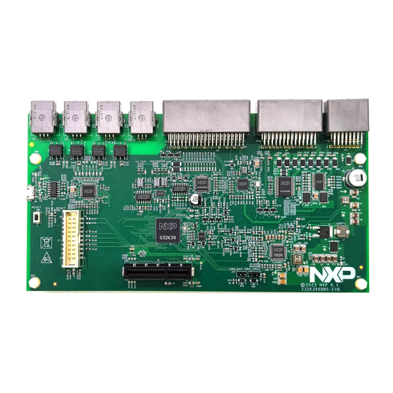
The document is a hardware and software user manual for the powertrain domain controller reference design integrated with the BMS and VCU in one ECU, based on the S32K376 MCU. The BMS system monitors battery voltage, temperature, fault status, and so on. VCU samples simulated pedal position, gear, sensors, and so on. - Page 3 • AFE MC33774 monitors battery status. • Gateway MC33665 transfers the SPI signal to TPL3. • SBC FS2633 supplies power for S32K376 and external devices. • HSD, LSD, and MSDI are used for VCU functions. • CAN, LIN, and UART communicate with other ECU.
-
Page 4: Board Features
2.3.1 Power SBC 2.3.1.1 Board power The PFS2633 provides robust, scalable power management to the S32K376 MCU with Fail Silent safety monitoring measures that fit for ASIL D. It features multiple switch mode regulators and LDO voltage regulators to supply the microcontroller, sensors, peripheral ICs, and communication interface. It offers a high-precision voltage reference available to the system and a reference voltage for two independent voltage-tracking regulators. -
Page 5: Debug Mode
UG10071 NXP Semiconductors S32K376 BMU and VCU Integration User Guide Figure 3. BMU power tree 2.3.1.2 Debug mode The jumper J1 configures the Debug mode of the SBC, enable it to active the Debug mode, and then there is no deep fail-safe state. It is recommended to be closed to J1, as in Figure 4 at the development phase. -
Page 6: Reset Circuit
UG10071 NXP Semiconductors S32K376 BMU and VCU Integration User Guide 2.3.1.3 Reset circuit When the specific condition is reached, the SBC resets MCU via the SBC_RSTB pin. As shown in Figure 5, the board supports the multiple MCU reset methods: SBC, JTAG, and Switch Reset(SW1). -
Page 7: Jtag Connector
UG10071 NXP Semiconductors S32K376 BMU and VCU Integration User Guide Figure 7. 40 MHz crystal circuit 2.3.4 JTAG connector The BMU board is fitted with a 20-pin JTAG debug connector J7. Figure 8 shows the 20-pin JTAG connector pinout. Figure 8. JTAG connector interface 2.3.5 USB/UART transceiver... -
Page 8: Can Transceiver
UG10071 NXP Semiconductors S32K376 BMU and VCU Integration User Guide Figure 9. USB/UART transceiver circuit 2.3.6 CAN transceiver The BMU board has two high speed CAN transceivers. • TJA1448ATK/0Z (U7) is a galvanically isolated interface between the CAN controller and the physical two- wire CAN bus and is connected to the MCU CAN0/CAN1 port (J15, K14, F11, F10). -
Page 9: Lin Transceiver
UG10071 NXP Semiconductors S32K376 BMU and VCU Integration User Guide Figure 11. TJA1145AT/FD/0Z transceiver circuit 2.3.7 LIN transceiver The BMU board is fitted with a TJA1022T LIN transceiver (U9) connected to MCU LPUART2 and LPUART3 ports (L13, M13, N13, N12). And the pins LIN_SLP1_N and LIN_SLP2_N must be high. -
Page 10: Saradc Interface
UG10071 NXP Semiconductors S32K376 BMU and VCU Integration User Guide Figure 13. TJA1101 ETH PHY circuit 2.3.9 SARADC interface The BMU board enables 6x SARADC channels from MCU_AIN0 to MCU_AIN5. These channels are routed to connectors to measure external analog signals, such as pedals, and sensor signals, through ADC input signal... -
Page 11: Msdi
UG10071 NXP Semiconductors S32K376 BMU and VCU Integration User Guide Figure 15. Digital input circuit 2.3.11 MSDI The BMU board has an MC33CD1030 to detect the closing and opening of multiple switch contacts and analog input signals. The input signal is transferred to the MCU through LPSPI3 with CS1. -
Page 12: Hsd
UG10071 NXP Semiconductors S32K376 BMU and VCU Integration User Guide Figure 17. PWM circuit 2.3.13 HSD The system requires several channels to drive an external load. Provide high current driving capability that could control these devices directly. Generally load as: • Main contactor - 12 V dc coil voltage rating, max 5 A coil current at ON. -
Page 13: Tpl Transceiver
UG10071 NXP Semiconductors S32K376 BMU and VCU Integration User Guide Figure 19. LSD circuit 2.3.15 TPL transceiver Since the high voltage of battery packs, isolation is more important. This reference design isolates power supply and communications. The MC33665 is a transceiver physical layer transformer driver designed to interface an MCU conveniently to a high-speed isolated communication network. -
Page 14: Rtc
UG10071 NXP Semiconductors S32K376 BMU and VCU Integration User Guide 2.3.16 RTC The real-time clock is necessary for the system's two main functions: • Provide an uninterrupted timer to the system as a reference. When the system is Low-Power mode, the time is recorded and statistical discharge. -
Page 15: Ecu Connector
UG10071 NXP Semiconductors S32K376 BMU and VCU Integration User Guide Figure 23. BMU board wake-up sources 2.5 ECU connector Table 2 lists all the connections to the BMU board interface connector. Table 2. Board interface connector details Connector Signal Description Connector Signal... - Page 16 UG10071 NXP Semiconductors S32K376 BMU and VCU Integration User Guide Table 2. Board interface connector details ...continued Connector Signal Description Connector Signal Description J10-6 KEY_ON_DIN MSDI SG0 J10-26 Digital GND J10-7 KEY_START_DIN MSDI SG5 J10-27 BRAKE_SW_DIN brake switch input J10-8 AC_SW_DIN...
-
Page 17: Software User Guide
UG10071 NXP Semiconductors S32K376 BMU and VCU Integration User Guide Table 3. ...continued Function Connector Signal Description OBC_PFC_PHASE_ADC ADC1_P0 PFC phase voltage OBC_PFC_BUS_ADC ADC1_P1 PFC output voltage OBC_PFC_CINPUT_ADC ADC1_P2 PFC input current OBC_PFC_CTH_ADC ADC5_P0 PFC upper-MOS drain current OBC_PFC_CTL_ADC... -
Page 18: Software Block Diagram
3.2 Software block diagram Figure 24 shows the S32k376 BMS and VCU solution software block diagram. BMS function runs on function on core CM7_0, VCU function runs on lockstep on core CM7_2 and monitors another two cores through IPCF. OTA and reserved OBC functions run on the function core CM7_1. Bootloader and OTA for updating firmware. -
Page 19: Bms Program Flow
UG10071 NXP Semiconductors S32K376 BMU and VCU Integration User Guide Figure 25. MCAL demo project programming flow diagram • BMS tasks run on Core0, scheduled by general timer. • OTA tasks run on Core1, scheduled by FreeRTOS. • VCU and BSP tasks, run on Core2, scheduled by general timer. -
Page 20: Saf Function
UG10071 NXP Semiconductors S32K376 BMU and VCU Integration User Guide Figure 26. BMS program flow Regarding the running state machine, there are five major cycles. Each cycle has ten minor cycles. The major cycle increase one after the minor cycle increase to ten cycles. -
Page 21: Bms Sl Function
3.7 Project memory map S32K376 have 6M flash space to store code binary that consists of three 2M flash blocks. The bootloader is placed in the first flash block, and the three core projects are divided into one flash block via link file and MPU. -
Page 22: Software And Tools Required
UG10071 NXP Semiconductors S32K376 BMU and VCU Integration User Guide Figure 28. Memory map 3.8 Software and tools required • Configuration tool: EB Tresos Studio 29.0.0. • MCAL drivers: SW32K3_RTD_4.4_R21-11_3.0.0_P01. • BMS CDD: SWS32K3_BMS_SDK_4.4_1.0.0 • Compiler: GCC version 10.2.0 20200723. • Debugger: Lauterbach TRACE32 JTAG Debugger. -
Page 23: How To Build
UG10071 NXP Semiconductors S32K376 BMU and VCU Integration User Guide Figure 29. Lauterbach debugger Figure 30. PCAN-USB Pro 3.9 How to build 1. Open EB Tresos Studio and import EB Tresos project. There are three cores project to split-up CM7_0, CM7_1, and lockstep core CM7_2. -
Page 24: How To Download.elf File
UG10071 NXP Semiconductors S32K376 BMU and VCU Integration User Guide Figure 32. Generation of source file 3. Fill in the user-defined paths for compilation in project_parameters.mk, at each project. Normally, the user must only modify the GCC_DIR path to the user’s location; other paths have been set to a relative path. The other two projects must perform the same operation. -
Page 25: Ota
UG10071 NXP Semiconductors S32K376 BMU and VCU Integration User Guide 2. Select S32K376_flash_triple_core012.cmm (in S32K376_BMSVCU/debug directory) to download all 3x project.elf files into flash. 3. When the debugger finishes loading.elf into flash, it pops out three debug windows corresponding to each project. -
Page 26: Ota Memory Map
UG10071 NXP Semiconductors S32K376 BMU and VCU Integration User Guide Figure 38. OTA code flash memory layout 1. The OTA update agent-APP_V1 is first downloaded to the active block1 (0x00600000) via the debugger and then starts running. 2. When the OTA update is performed, PC sends the new version of the OTA update agent-APP_V2, APP_V1 receives the binary file of APP_V2, and writes it to the block2(0x0800000), which is in passive. - Page 27 UG10071 NXP Semiconductors S32K376 BMU and VCU Integration User Guide • Connect BMU through Ethernet, and modify the IP address of the PC to an unused address in the 192.168.0.x network segment showing in the blew Figure 40 Figure 40. IP address Configuration of PC 2.
- Page 28 UG10071 NXP Semiconductors S32K376 BMU and VCU Integration User Guide Figure 42. ECUBus Project folder 6. Configuration of Ethernet communication. • Click the settings button in the upper right corner. • Input Multicast as 192.168.0.255, SA (source address) as 55. • Click Search Device, then click Connect.
- Page 29 UG10071 NXP Semiconductors S32K376 BMU and VCU Integration User Guide Figure 43. Configuration parameter of Ethernet 7. Preparation of update binary. Change the directory to S32K376_BMSVCU/ota_tool/merge_bin. Execute mergebin_ota.bat. It merges three project binaries into one binary. Select Address as S32K396-HW- OTA_V0. Then change the ECUBus service info 10th item, click the "Choose File" button, select the previously merged binary, and click the "Change Group"...
-
Page 30: Bootloader User Guide
UG10071 NXP Semiconductors S32K376 BMU and VCU Integration User Guide Figure 44. Configuration of the download file 8. Execute the OTA procedure. • Click the start button. • Wait for the binary to be downloaded successfully, and the code automatically runs after the download is complete. -
Page 31: How To Debug
UG10071 NXP Semiconductors S32K376 BMU and VCU Integration User Guide • Determine whether to enter bootloader mode by detecting the J10_27 and J10_32 status. If both J10_27 and J10_32 are 12 V high voltage, enter bootloader mode. 5.2 How to debug 1. - Page 32 UG10071 NXP Semiconductors S32K376 BMU and VCU Integration User Guide Figure 47. ECUBus UDS project folder 6. Configuration of CANFD communication. • Click the settings button in the upper right corner. • CAN-FD: Select the device, then check CAN-FD and check PADDING. Select the nominal bit rate as 500 kbit/s, the data bit rate as 2 Mbit/s, and TLC as 64.
- Page 33 UG10071 NXP Semiconductors S32K376 BMU and VCU Integration User Guide Figure 48. Configuration parameter of CANFD 7. Preparation of update binary. • Change the directory to S32K376_BMSVCU/ota_tool/merge_bin. Execute mergebin_ota.bat. It merges three project binaries into one binary. • Checked defaultName1 in the address box.
-
Page 34: Gui User Guide
UG10071 NXP Semiconductors S32K376 BMU and VCU Integration User Guide Figure 49. Configuration of the download file 8. Execute the OTA procedure. • Click the start button. • Wait for the binary to be downloaded successfully. • Press SW1 to reset BMU, the APP has installed in the flash bock1, and the code always jumps to block1 to execute the APP when the code starts. - Page 35 UG10071 NXP Semiconductors S32K376 BMU and VCU Integration User Guide Figure 51. GUI layout Info 1. Select the CAN port and baud rate (500 kbit/s for this demo) of CAN transmission then click the Start button. Click the Stop button when you want to disconnect the CAN adapter.
-
Page 36: Gui Data Can Protocol
UG10071 NXP Semiconductors S32K376 BMU and VCU Integration User Guide Figure 52. BCC data table page 6.2 GUI data CAN protocol The following figure lists all the protocols that interact data between GUI and BMU. The ID 0x1881xxxx to 0x1887xxxx are used for BMS data, and the ID 0x1889xxxx is used for VCU communication. Customers can parse those data on either PCAN viewer. -
Page 37: Revision History
UG10071 NXP Semiconductors S32K376 BMU and VCU Integration User Guide Figure 53. GUI interaction protocol 7 Revision history Table 5. Revision history Document ID Release date Description UG10071 v.1.1 15 January 2024 Added IPCF UG10071 v.1.0 5 June 2023 Initial release UG10071 All information provided in this document is subject to legal disclaimers. -
Page 38: Legal Information
NXP Semiconductors. NXP and its suppliers shall not be liable for any such use by customer. In no event shall NXP Semiconductors be liable for any indirect, incidental, Accordingly, customer will indemnify and hold NXP harmless from any... - Page 39 UG10071 NXP Semiconductors S32K376 BMU and VCU Integration User Guide Tables Tab. 1. List of acronyms ..........2 Tab. 4. MCAL Project Files ......... 18 Tab. 2. Board interface connector details ....15 Tab. 5. Revision history ..........37 Tab. 3................16 Figures Fig.
-
Page 40: Table Of Contents
UG10071 NXP Semiconductors S32K376 BMU and VCU Integration User Guide Contents Introduction ............2 Acronyms ............2 Hardware user guide .......... 2 Overview ............2 Board features ........... 4 Module introduction ........... 4 2.3.1 Power SBC ............4 2.3.1.1 Board power ............4 2.3.1.2...
Need help?
Do you have a question about the S32K376 and is the answer not in the manual?
Questions and answers