Table of Contents
Advertisement
Quick Links
NXP Semiconductors
User Guide
S32G-VNP-EVB3 User Guide
by: NXP Semiconductors
1. Introduction
S32G is a high-performance vehicle network processor
that combines controller area network (CAN), local
interconnect network (LIN), and FlexRay networking
with high data-rate Ethernet networking. It also
combines a functional safe-core infrastructure with
MPU cores, and includes high level security features.
A platform for software development on S32G is
available from NXP, named the S32G Vehicle Network
Processor Evaluation Board (S32G-VNP-EVB3). This
hardware supports the most common S32G use cases
primarily by enabling the communication interfaces to
allow users to rapidly prototype software using the
features of S32G-VNP-EVB3.
This user guide provides detailed reference for usage of
the S32G-VNP-EVB3. This includes detailed board
configuration including connectors, jumpers, LED
indicators and S32G on-board programming.
Document Number: S32GVNPEVB3UG
Contents
1.
Introduction .................................................................... 1
2.
S32G-VNP-EVB3 Hardware Kit Contents ....................... 2
3. S32G-VNP-EVB3 Details.................................................... 3
3.1 Power connections from PMIC to S32G ........................ 3
3.2 Power connections for S32G-VNP-EVB3...................... 3
EVB3.................................................................4
3.4 Peripheral addressing table of S32G-VNP-EVB3 ........... 4
3.5 S32G-PROCEVB3-S overview ..................................... 6
3.6 S32GRV-PLATEVB-S Overview ............................... 14
3.5 Viewing console logs over UART ............................... 22
4. Debugger Connections....................................................... 23
4.1 Lauterbach ................................................................. 23
4.2 S32 debug probe ......................................................... 24
4.3 Aurora based debugger ............................................... 26
5. S32G-VNP-EVB3 Software ............................................... 29
6. Interfaces Block Diagram .................................................. 30
6.1 CAN interface ............................................................ 30
6.2 LIN interface .............................................................. 31
6.3 FlexRay interface ....................................................... 31
6.4 DSPI interface ............................................................ 32
6.5 I2C interface .............................................................. 34
6.6 RGMII interface ......................................................... 34
6.7 SERDES interface ...................................................... 35
6.8 QSPI controller .......................................................... 36
6.9 uSDHC controller ....................................................... 37
6.10 USB ULPI controller ................................................ 37
6.11 LPDDR4 controller................................................... 38
6.12 OpenSDA controller ................................................. 38
Support Multiple Configurations .................................... 40
7.1 External clock using SMA connector........................... 40
7.2 Use of KSZ PHY ........................................................ 40
7.3 Using Ethernet card .................................................... 41
Rev. 0 , 11/2021
Advertisement
Table of Contents

Related Manuals for NXP Semiconductors S32G-VNP-EVB3


Summary of Contents for NXP Semiconductors S32G-VNP-EVB3
-
Page 1: Table Of Contents
3.3 Part numbers of memories and PHY on S32G-VNP- EVB3………………………………………………………..4 MPU cores, and includes high level security features. 3.4 Peripheral addressing table of S32G-VNP-EVB3 ... 4 3.5 S32G-PROCEVB3-S overview ........6 A platform for software development on S32G is 3.6 S32GRV-PLATEVB-S Overview ....... 14 available from NXP, named the S32G Vehicle Network 3.5 Viewing console logs over UART ....... -
Page 2: S32G-Vnp-Evb3 Hardware Kit Contents
3. S32G-VNP-EVB3 Details 2. S32G-VNP-EVB3 Hardware Kit Contents The following table lists the items included in the S32G-VNP-EVB3 hardware kit Table 1. Items included in hardware kit Item Description Quantity S32GRV-PLATEVB Platform board S32G-PROCEVB3-S Processor board Power Supply 12 V,6.67 A AC-DC power supply,... -
Page 3: S32G-Vnp-Evb3 Details
3. S32G-VNP-EVB3 Details 3. S32G-VNP-EVB3 Details S32G-VNP-EVB3 is a combination of two boards • S32G-PROCEVB3-S – the processor board • S32GRV-PLATEVB – the platform board 3.1 Power connections from PMIC to S32G Refer to section “Power Connections” in device Hardware Design Guidelines for power supply connections from PMIC VR5510 to S32G. -
Page 4: Part Numbers Of Memories And Phy On S32G-Vnp-Evb3
USB UPLPI USB ULPI PHY USB83340AM AURORA Connector ASP-130367-01 3.4 Peripheral addressing table of S32G-VNP-EVB3 3.4.1 MDC/MDIO address table The following table describes the MDC/MDIO address for peripherals on S32G-VNP-EVB3. S32G-VNP-EVB3 User Guide, Rev. 0, 11/2021 NXP Semiconductors COMPANY CONFIDENTIAL... - Page 5 S32G- KSZ9031RNXCA 0x4 PROCEVB3-S PFE_MAC2 S32GRV- Add on board Add on board PLATEVB connector 3.4.2 I2C address table The following table describes the I2C address on S32G-VNP-EVB3. Table 4. I2C address Peripherals Location Reference Device Address Destination I2C_0 S32G-PROCEVB3- AT24C01B...
-
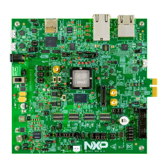
Page 6: S32G-Procevb3-S Overview
Table 4. Boot mode configuration Boot Mode SW14[1:2] SW15[1:2] Boot from RCON (S32G-VNP- EVB3 is set to SD boot mode by default) Boot from Serial S32G-VNP-EVB3 User Guide, Rev. 0, 11/2021 NXP Semiconductors COMPANY CONFIDENTIAL... - Page 7 Resets S32G Connects to S32G Reset line S32G POR Applies POR to S32G Connects to S32G POR line SMA connector External clock input Connects external clock source to S32G- interface VNP-EVB3 S32G-VNP-EVB3 User Guide, Rev. 0, 11/2021 NXP Semiconductors COMPANY CONFIDENTIAL...
- Page 8 P1_8V_IO_USB On: Connects P1_8V_ANA to P1_8V_IO_USB (default) J162 P3_3V_STBY_MCU Off: Disconnects P3_3V_STBY_BRD to (VDD_IO_STBY voltage) P3_3V_STBY_MCU On: Connects P3_3V_STBY_BRD to P3_3V_STBY_MCU (default) J152 Source Selection for 1-2: Connects P1_8V_ANA to S32G-VNP-EVB3 User Guide, Rev. 0, 11/2021 NXP Semiconductors COMPANY CONFIDENTIAL...
- Page 9 JTAG_TMS 1-2: Enables TMS For JTAG (default) 2-3: Enables TMS for SWD (Serial wire debug) J154 JTAG_TDI 1-2: Enables TDO for JTAG (default) 2-3: Enables TDI for SWD (Serial wire S32G-VNP-EVB3 User Guide, Rev. 0, 11/2021 NXP Semiconductors COMPANY CONFIDENTIAL...
- Page 10 4-6: Selects PC_10 (CC LIN 0 RX) to LIN0_RX J155 Selects the path to route CAN 0 1-3: Routes CAN 0_RX on S32G- PROCEVB3-S (default) 2-4: Routes CAN 0_TX on S32G- S32G-VNP-EVB3 User Guide, Rev. 0, 11/2021 NXP Semiconductors COMPANY CONFIDENTIAL...
- Page 11 Off: Disconnects fail safe output signal from VR5510 to S32G (default) On: Connects fail safe output signal from VR5510 to S32G Selection pin between USB HOST Off: USB behaves as USB DEVICE S32G-VNP-EVB3 User Guide, Rev. 0, 11/2021 NXP Semiconductors COMPANY CONFIDENTIAL...
- Page 12 1-2: Configures the output as(default): OUT0: 100 MHz OUT1: 100 MHz OUT2: 25 MHz OUT3: 26 MHz OUT4: 125 MHz OUT5: 100 MHz 2-3: Configures the output as: OUT0: 100 MHz OUT1: 100 MHz S32G-VNP-EVB3 User Guide, Rev. 0, 11/2021 NXP Semiconductors COMPANY CONFIDENTIAL...
- Page 13 On: Connects P12V from VR5510 to 12 V voltage (default) Source Selection for 5 V voltage Off: Connects VBOOST_5V from VR5510 to 12 V voltage On: Connects VBOOST_5V from VR5510 to 12 V voltage (default) S32G-VNP-EVB3 User Guide, Rev. 0, 11/2021 NXP Semiconductors COMPANY CONFIDENTIAL...
-
Page 14: S32Grv-Platevb-S Overview
Activity present on Tx line of UART1 to Green General purpose LED General purpose Green General purpose LED General purpose 3.6 S32GRV-PLATEVB-S Overview The S32G-PROCEVB3-S is stacked over the S32GRV-PLATEVB as shown below: S32G-VNP-EVB3 User Guide, Rev. 0, 11/2021 NXP Semiconductors COMPANY CONFIDENTIAL... - Page 15 PLATEVB in stacked mode refer to attachments. 3.6.1 S32G-PROCEVB3-S Connections to the S32GRV-PLATEVB The connections from S32G-PROCEVB3-S to the S32GRV-PLATEVB can be referred from the schematics as shown below: S32G-PROCEVB3-S <-> S32GRV-PLATEVB 1. J1<->J80 connection S32G-VNP-EVB3 User Guide, Rev. 0, 11/2021 NXP Semiconductors COMPANY CONFIDENTIAL...
- Page 16 3. S32G-VNP-EVB3 Details Figure 5. J1<->J80 connection 1. J2<->J66 connection Figure 6. J2<->J66 connection S32G-VNP-EVB3 User Guide, Rev. 0, 11/2021 NXP Semiconductors COMPANY CONFIDENTIAL...
- Page 17 3. S32G-VNP-EVB3 Details 1. J3<->J81 connection Figure 7. J3<->J81 connection 1. J4<->J87 connection Figure 8. J4<->J87 connection S32G-VNP-EVB3 User Guide, Rev. 0, 11/2021 NXP Semiconductors COMPANY CONFIDENTIAL...
- Page 18 Arduino Connector -open- connector Arduino Connector -open- connector ADC connector Voltage source J114 Aquantia 3-pin Aquantia connector Connects to Aquantia Probe to Connector program Aquantia firmware Via SJA1105Q automotive Ethernet switch S32G-VNP-EVB3 User Guide, Rev. 0, 11/2021 NXP Semiconductors COMPANY CONFIDENTIAL...
- Page 19 To enable CAN 12, CAN 13 1-2: Enables CAN12_RX (default) 3-4: Enables CAN12_TX (default) 5-6: Enables CAN13_RX (default) 7-8: Enables CAN13_TX (default) To enable CAN 14 Tx Off: Disables CAN14_TX S32G-VNP-EVB3 User Guide, Rev. 0, 11/2021 NXP Semiconductors COMPANY CONFIDENTIAL...
- Page 20 Off: Disables GE PHY2 INT On: Enables GE PHY2 INT (default) J106 To enable 12V_ENET Off: Disables 12V_ENET On: Enables 12V_ENET (default) To enable 3V3_ECARD Off: Disables 3V3_ECARD On: Enables 3V3_ECARD (default) S32G-VNP-EVB3 User Guide, Rev. 0, 11/2021 NXP Semiconductors COMPANY CONFIDENTIAL...
- Page 21 On: Enables 1V8_RGMII3_DVDD (default) J116 To enable 1V2_RGMII3_VDDL Off: Disables 1V2_RGMII3_VDDL of U43 On: Enables 1V2_RGMII3_VDDL (default) J117 To enable 3V3_RGMII3_AVDD Off: Disables 3V3_RGMII3_AVDD of U43 On: Enables 3V3_RGMII3_AVDD (default) S32G-VNP-EVB3 User Guide, Rev. 0, 11/2021 NXP Semiconductors COMPANY CONFIDENTIAL...
-
Page 22: Viewing Console Logs Over Uart
Connect a micro USB cable from host PC to J58 on S32G-PROCEVB3-S for viewing console logs over UART0 and J179 for console logs over UART1. Figure 9. Viewing console logs S32G-VNP-EVB3 User Guide, Rev. 0, 11/2021 NXP Semiconductors COMPANY CONFIDENTIAL... -
Page 23: Debugger Connections
This section shows the hardware connection setup required to connect the debugger to S32G- PROCEVB3-S. 4.1 Lauterbach Lauterbach’s PowerDebug USB allows to debug and control the system on the S32G-VNP-EVB3 using T32 software. To attach the 20-pin Lauterbach cable on S32G-PROCEVB3-S, follow the below steps: 1. -
Page 24: S32 Debug Probe
4.2 S32 debug probe Attached is the complete image of the S32 debug probe with included accessories (Ethernet cable is shown but not included in the kit). Figure 11. S32G debug probe package S32G-VNP-EVB3 User Guide, Rev. 0, 11/2021 NXP Semiconductors COMPANY CONFIDENTIAL... - Page 25 4. Debugger Connections Figure 12. Connecting S32 Debug probe on S32G-VNP-EVB3 Following are the details of the S32 Debug Probe: • Debug probe: S32DBGPROBE • Debug cable: ARM ® 20-pin probe tip and ribbon cable (included in S32DBGPROBE kit) To attach the ARM 20-pin probe tip and ribbon cable to S32G-PROCEVB3-S, follow the below steps: 1.
-
Page 26: Aurora Based Debugger
4. Connect the 40-pin Aurora Trace probe(ATP) to Aurora header J26 on S32G-PROCEVB3-S. Figure 13. Aurora Port setup 1 with ATP and JTAG cable connected on S32G-VNP-EVB3 Aurora port also supports JTAG debug capabilities which can be used by doing below hardware modification on S32G-PROCEVB3-S: •... - Page 27 2. Connect the cable from Lauterbach to PC. 3. Connect the 20-pin JTAG cable to the JTAG header Aurora based debugger. 4. Connect the 40-pin Aurora Trace probe(ATP) to the Aurora header J26 on S32G-PROCEVB3-S. S32G-VNP-EVB3 User Guide, Rev. 0, 11/2021 NXP Semiconductors COMPANY CONFIDENTIAL...
- Page 28 5. S32G-VNP-EVB3 Software Figure 15. Aurora Port setup 1 with only ATP cable connected to S32G-VNP-EVB3 S32G-VNP-EVB3 User Guide, Rev. 0, 11/2021 NXP Semiconductors COMPANY CONFIDENTIAL...
-
Page 29: S32G-Vnp-Evb3 Software
6. Interfaces Block Diagram 5. S32G-VNP-EVB3 Software All NXP releases for S32G are supported on S32G-VNP-EVB3. Refer the product page for more details on SW releases. S32G-VNP-EVB3 User Guide, Rev. 0, 11/2021 NXP Semiconductors COMPANY CONFIDENTIAL... -
Page 30: Interfaces Block Diagram
The block diagram for various interfaces are shown in below subsections where blue boxes represent the interfaces present on S32G-PROCEVB3-S and yellow boxes represent the interfaces present on S32G- PLATEVB. 6.1 CAN interface The following figure shows the CAN signals on S32G-VNP-EVB3. CAN PHY CAN0TX/CAN0RX S32G... -
Page 31: Lin Interface
6. Interfaces Block Diagram 6.2 LIN interface The following diagram shows the LIN/UART2USB signals on S32G-VNP-EVB3. SPI I/F LIN PHY PC07,PL07 CONNECTOR PC9,PC10 LIN0_TX/RX (PFE_UART) LIN0_TX/RX 87/85 LIN1_TX/RX 87/85 PK15,PL00 (LLCE_0/ LINFlex_0) UART0_TX/RX UART2USB TJA1024HG CONN. CONNECTOR GPIO_J2/01_03 LINTX2/RX2 LIN1_TX/RX... -
Page 32: Dspi Interface
FLXR0A_RXD FLEXRAY FLXR0B_TXEN FLXR0B_TXEN PL_04 TJA1081 FLXR0B_TXD FLXR0B_TXD PL_05 FLXR0B_RXD PL_06 FLXR0B_RXD Figure 18. FlexRAY interfacing with S32G-VNP-EVB3 6.4 DSPI interface The following figure shows the DSPI signals on S32G-VNP-EVB3. S32G-VNP-EVB3 User Guide, Rev. 0, 11/2021 NXP Semiconductors COMPANY CONFIDENTIAL... - Page 33 SS_b DSPI_4 ENET CARD S32G UART_TX_PC09 CONNECTOR PC_09 SPI_SCK_S1SB SPI_SCK_S1SB SPI_SIN_S1SB SPI_MISO_S1SB PC_10 UART_RX_PC10 SPI_MOSI_S1SB SPI_SOUT_S1SB PB_09 FLEXCAN3_TX RCON BUFF SPI_CS_S1SB SPI_CS_S1SB PB_10 FLEXCAN3_RX Figure 19. DSPI interfacing with S32G-VNP-EVB3 S32G-VNP-EVB3 User Guide, Rev. 0, 11/2021 NXP Semiconductors COMPANY CONFIDENTIAL...
-
Page 34: I2C Interface
GPIO_J13-04 PC_01/PC_02 GPIO34_I2C4_SCL CONNECTOR RCON BUFF ARDUINO CONNECTOR VR5510 PF53 0x20 0x40 Figure 20. I2C interfacing with S32G-VNP-EVB3 6.6 RGMII interface The following diagram shows the RGMII signals on S32G-VNP-EVB3. S32G-VNP-EVB3 User Guide, Rev. 0, 11/2021 NXP Semiconductors COMPANY CONFIDENTIAL... -
Page 35: Serdes Interface
PFE_MAC2) 3.3V MII_3 RGMII PHY KSZ9031RNX 3.3V MII_4 RGMII PHY KSZ9031RNX Figure 21. RGMII signal path on S32G-VNP-EVB3 6.7 SERDES interface The following diagram shows the SERDES interface on S32G-VNP-EVB3. S32G-VNP-EVB3 User Guide, Rev. 0, 11/2021 NXP Semiconductors COMPANY CONFIDENTIAL... -
Page 36: Qspi Controller
SERDES0_LANE 1 MUX/ DMUX MUX/ CONNECTOR AQR107 DMUX SERDES1_LANE 1 S32G Figure 22. SERDES interface on S32G-VNP-EVB3 6.8 QSPI controller The following diagram shows S32G connections to QSPI controller on S32G-VNP-EVB3. S32G QSPI QSPI_DATA[0:7] P1_8V_IO_QSPI RESET_B QSPI_A_DQS QSPI_A_SCK P1_8V_IO_QSPI QSPI_A_CS0 P1_8V_IO_QSPI Figure 23. -
Page 37: Usdhc Controller
EMMC_CLK EMMC_CMD eMMC EMMC_RST EMMC_DQS Figure 24. S32G connections to uSDHC controller on S32G-VNP-EVB3 6.10 USB ULPI controller The following diagram shows S32G connections to USB ULPI controller on S32G-VNP-EVB3. USB_DP/N USB CONN. MICRO AB S32G USB_D[0:7] ULPI PHY USB83340... -
Page 38: Lpddr4 Controller
6. Interfaces Block Diagram 6.11 LPDDR4 controller The following diagram shows S32G connections to LPDDR4 controller on S32G-VNP-EVB3. P1_1V DDR_CA_A[0:5] LPDDR4 DDR_ODT_CA_A (DDR_CLKA_T, DDR_CLKA_C) DDR_CKE0_A DDR_CKE1_A DDR_CS0_A DDR_CS1_A RANK A DQ[0:7] DQ[0:7] DMI0 DMI_0 DQS0_P/N DQS0_T/C DQ[8:15] DQ[8:15] DMI1 DMI_1... - Page 39 7.Hardware Modifications required on S32G-VNP-EVB3 to Support Multiple Configurations S32G 3V3_BRD REG_OUT P3V3_SDA VDDIO_SDA J_TCK SDA_SWD_EN JTAG_TCK CONNECTOR PA_04/TCK LEVEL SHIFTER SDA_SWD_SCK CONN J_TMS SDA_SWD_OE JTAG_TMS PA_05/TMS LEVEL SHIFTER SDA_SWD_DOUT CONN LIN0_TX OPENSDA_UART_RX LIN0_TX CONN LEVEL SHIFTER J_TDI MK26F SDA_SWD_DIN...
-
Page 40: Hardware Modifications Required On S32G-Vnp-Evb3 To Support Multiple Configurations
7.Hardware Modifications required on S32G-VNP-EVB3 to Support Multiple Configurations 7.Hardware Modifications required on S32G-VNP-EVB3 to Support Multiple Configurations The following sections provides information on hardware modifications required on S32G-VNP-EVB3 to support multiple configurations. 7.1 External clock using SMA connector To use external clock using SMA connector, instead of default crystal do the following hardware modifications on S32G-PROCEVB3-S: 1. -
Page 41: Using Ethernet Card
7.Hardware Modifications required on S32G-VNP-EVB3 to Support Multiple Configurations Figure 29. Schematics snapshot showing default position of J129 Figure 30. Schematics snapshot showing default position of R579 to R590 7.3 Using Ethernet card To use an ethernet card on SABRE connector present on S32G-PLATEVB, instead of default USB ULPI PHY on S32G-PROCEVB3-S, do the following hardware modifications on S32G-PROCEVB3-S. - Page 42 7.Hardware Modifications required on S32G-VNP-EVB3 to Support Multiple Configurations Move 0 resistor from position A (1-2) to position B (3-2) for R555 to R566. Figure 31. Schematics snapshot showing default position of R555 to R566 S32G-VNP-EVB3 User Guide, Rev. 0, 11/2021...
- Page 43 7.Hardware Modifications required on S32G-VNP-EVB3 to Support Multiple Configurations S32G-VNP-EVB3 User Guide, Rev. 0, 11/2021 NXP Semiconductors COMPANY CONFIDENTIAL...
- Page 44 Information in this document is provided solely to enable system and software How to Reach Us: implementers to use NXP products. There are no express or implied copyright licenses Home Page: granted hereunder to design or fabricate any integrated circuits based on the nxp.com information in this document.
Need help?
Do you have a question about the S32G-VNP-EVB3 and is the answer not in the manual?
Questions and answers