Table of Contents
Advertisement
Quick Links
Table of Contents
1
Introduction ......................................................................................................................................................................... 2
2
Features .............................................................................................................................................................................. 3
3
Top Level Block Diagram .................................................................................................................................................... 4
3.1. EVB Starter Guide ................................................................................................................................................... 4
4
Jumper Default List ............................................................................................................................................................. 7
5
Status LEDs ........................................................................................................................................................................ 7
2
6
C/SPI On Board/External Configuration ............................................................................................................................ 8
7
SiT9531x EVK Board Power Supply Connection Details .................................................................................................... 8
7.1. VDDIN and VDDOX Supply Regulator..................................................................................................................... 8
7.2. VDD Supply Regulator ............................................................................................................................................. 9
7.3. GPIO_VDD Supply Regulator ................................................................................................................................ 10
8
External Clock Reference Input (X1/X2) ............................................................................................................................ 11
9
Input Clock Circuitry (INx_P/INx_N) .................................................................................................................................. 12
10
Output Clock Circuitry (OUTxP/OUTxN) ........................................................................................................................... 13
11
GPIO Configuration ........................................................................................................................................................... 14
12
EEPROM Configuration .................................................................................................................................................... 15
13
MSP430 Programming Instructions ................................................................................................................................... 15
MSP430 Programming Procedure .................................................................................................................................. 15
14
SiTime Clock GUI Installation and EVB Configuration ...................................................................................................... 17
SiT9531xEB User Manual | Rev 0.5
SiT9531x Evaluation Board (EVB) HW
User Manual
Page 1 of 18
www.sitime.com
Advertisement
Table of Contents

Related Manuals for SiTime SiT9531 Series


Summary of Contents for SiTime SiT9531 Series
-
Page 1: Table Of Contents
Output Clock Circuitry (OUTxP/OUTxN) ........................... 13 GPIO Configuration ................................14 EEPROM Configuration ..............................15 MSP430 Programming Instructions ........................... 15 MSP430 Programming Procedure ..........................15 SiTime Clock GUI Installation and EVB Configuration ...................... 17 SiT9531xEB User Manual | Rev 0.5 Page 1 of 18 www.sitime.com... -
Page 2: Introduction
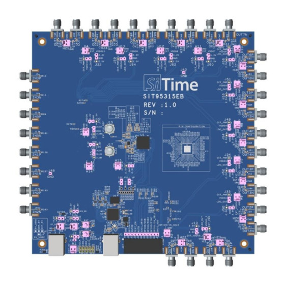
1 Introduction The SiT53XX Evaluation Board is designed for evaluating the SiT9531x family of Quad PLL Frequency Translator, Jitter Cleaner. • SiT95315 • SiT95316 Figure 1. SiT9531x Evaluation Board SiT9531xEB User Manual | Rev 0.5 Page 2 of 18 www.sitime.com... -
Page 3: Features
Support LVPECL, CML, HCSL, LVDS and LVCOMS Output Standards Status LEDs for power supplies C or SPI communication via MS430 MCU On board LDO’s with configurable jumpers for all Power supplies SiT9531xEB User Manual | Rev 0.5 Page 3 of 18 www.sitime.com... -
Page 4: Top Level Block Diagram
3.1. EVB Starter Guide Power up the SiT9531x EVB using 5 V Supply from a USB cable connected to the PC where the SiTime Clock GUI is installed. All the supplies on board are powered from the on board USB connector. There are 2 USB connectors on the SiT9531x EVK. - Page 5 The default Jumper configuration is already done on the EVK board (Refer to Table 1) Launch the SiTime Clock GUI Software. (Refer to SiTime Clock GUI User Guide for more information) 2) Default Output Driver Configuration is LVDS and Output Driver Supplies are configured to 3.3 V 3) Default Supply for VDD =1.8 V and VDDIN = 3.3 V...
- Page 6 SiT9531x Evaluation Board (EVB) HW User Manual Figure 3. EVB Starter Connection Diagram SiT9531xEB User Manual | Rev 0.5 Page 6 of 18 www.sitime.com...
-
Page 7: Jumper Default List
5 Status LEDs Table 2. Status LED Indication Location Color Status Indication Green 5V Additional USB Power Green 5V Main USB Power Green MSP430 LDO Power Figure 4. Status LEDs SiT9531xEB User Manual | Rev 0.5 Page 7 of 18 www.sitime.com... -
Page 8: C/Spi On Board/External Configuration
SiT9531x Evaluation Board (EVB) HW User Manual C/SPI On Board/External Configuration The SiT9531x chip can be configured to communicate with I C and SPI 4 Wire with SiTime SiT9531x Clock GUI. The default EVK configuration will enable the I C communication with the chip. -
Page 9: Vdd Supply Regulator
1. 3.3 V - Connect the 3-Pin Jumper from 2 to 3. 2. 2.5 V - Connect the 3-Pin Jumper from 1 to 2. 3. 1.8 V - Remove the Jumper. VDD should be configured to 1.8 V by default. SiT9531xEB User Manual | Rev 0.5 Page 9 of 18 www.sitime.com... -
Page 10: Gpio_Vdd Supply Regulator
3. 1.8 V - Remove the Jumper. GPIO_VDD is configured to 1.8 V by default. VDDIO can either be configured to VDD or VDDIN, GPIO_VDD should always track the VDDIO supply. SiT9531xEB User Manual | Rev 0.5 Page 10 of 18 www.sitime.com... -
Page 11: External Clock Reference Input (X1/X2)
For changing from SiT30100 oscillator to external reference clock configuration, uninstall R310(0 Ω) and install C31(1 uF). Refer to the SiT9531x family of parts datasheet for the XO Pathway connection options. Figure 8. External Reference Connection SiT9531xEB User Manual | Rev 0.5 Page 11 of 18 www.sitime.com... -
Page 12: Input Clock Circuitry (Inx_P/Inx_N)
Differential AC Coupled (with the default EVK Input Termination Connection) Refer to the SiT9531x family of parts datasheet for the Single Ended and Differential Input Termination connection information. Figure 9. Input Clock Termination Circuit SiT9531xEB User Manual | Rev 0.5 Page 12 of 18 www.sitime.com... -
Page 13: Output Clock Circuitry (Outxp/Outxn)
In case DC coupling is required, the AC coupling capacitors (for ex- C96 & C99) can be replaced by a 0 ohm resistor. Refer to the SiT9531x datasheet for the Output Termination Connection information. Figure 10. Output Clock Termination Circuit SiT9531xEB User Manual | Rev 0.5 Page 13 of 18 www.sitime.com... -
Page 14: Gpio Configuration
J37, R150 needs to be removed. The GPIO status can be manually measured using the berg pin connectors placed near to the J37 switch for each of the GPIO’s. Figure 11. GPIO Control Status SiT9531xEB User Manual | Rev 0.5 Page 14 of 18 www.sitime.com... -
Page 15: Eeprom Configuration
3. Connect the board to supply and USB using micro USB cable. Reset the chip by pressing ‘SW1’ and ‘SW2’ together. 4. This will take MSP430 to programming mode. 5. If MSP430 is not detected, then the GUI will appear as shown below: SiT9531xEB User Manual | Rev 0.5 Page 15 of 18 www.sitime.com... - Page 16 7. If the device (MSP430) is in Programming mode, then it shows as ready as shown below: 8. Go to File-> Open User Firmware option. Open the location where the firmware file is placed. C3_EchoToHost.txt SiT9531xEB User Manual | Rev 0.5 Page 16 of 18 www.sitime.com...
-
Page 17: Sitime Clock Gui Installation And Evb Configuration
10. Select the firmware. The tool should load the firmware into the MCU and and show a completion message as shown: 14 SiTime Clock GUI Installation and EVB Configuration SiTime SiT9531x Clock GUI provides an easy interface to verify the performance of chip in the lab. The GUI uses the MSP430 microcontroller for the USB to I C/SPI communication on the board, the MSP430 MCU related software drivers are also configured while installing the GUI. - Page 18 © SiTime Corporation February 2024. The information contained herein is subject to change at any time without notice. SiTime assumes no responsibility or liability for any loss, damage or defect of a Product which is caused in whole or in part by (i) use of any circuitry other than circuitry embodied in a SiTime product, (ii) misuse or abuse including static discharge, neglect or accident, (iii) unauthorized modification or repairs which have been soldered or altered during assembly and are not capable of being tested by SiTime under its normal test conditions, or (iv) improper installation, storage, handling, warehousing or transportation, or (v) being subjected to unusual physical, thermal, or electrical stress.
Need help?
Do you have a question about the SiT9531 Series and is the answer not in the manual?
Questions and answers