Table of Contents
Advertisement
Quick Links
SiT92113 Ultra Low Jitter Buffer Evaluation Kit User Guide
Table of Contents
1
Introduction ......................................................................................................................................................................... 2
2
Features .............................................................................................................................................................................. 2
3
Functional Description ......................................................................................................................................................... 3
3.1. VDD and VDDO Power Supplies ............................................................................................................................. 3
3.2. Clock Inputs ............................................................................................................................................................. 3
3.3. Clock States (Input vs Output States) ...................................................................................................................... 3
3.4. Output Enable .......................................................................................................................................................... 4
4
Power Supply Connections ................................................................................................................................................. 4
5
Setting Input Clock Select and Output Enable in the EVB................................................................................................... 6
6
Input Clock Configuration .................................................................................................................................................... 7
7
Configuring for Single ended AC coupled Input Clock ........................................................................................................ 8
7.1. Driving Clock Inputs with LVCMOS Driver (AC coupled) ......................................................................................... 8
8
Configuring EVB for DC Coupled Input LVCMOS Clock ..................................................................................................... 9
8.1. Driving Clock Inputs with LVCMOS Driver (DC coupled) ......................................................................................... 9
8.2. EVB Changes for Driving Clock Inputs with LVCMOS Driver (DC coupled, single ended) ...................................... 9
9
Driving Differential LVDS or LVDS Boost (AC coupled) .................................................................................................... 11
10
Board Configuration for driving DC Coupled LVDS ........................................................................................................... 12
10.1. LVDS (DC coupled) ............................................................................................................................................... 12
10.2. Board Changes Required for DC Coupled LVDS .................................................................................................. 12
11
Board Configuration Required for Driving DC/AC coupled LVPECL ................................................................................. 13
11.1. DC/AC Coupled LVPECL ....................................................................................................................................... 13
12
EVB Snapshot ................................................................................................................................................................... 14
13
PCB Schematic ................................................................................................................................................................. 15
13.1. Schematic Sheet 1 ................................................................................................................................................. 15
13.2. Schematic Sheet 2 ................................................................................................................................................. 16
13.3. Schematic Sheet 3 ................................................................................................................................................. 17
13.4. Schematic Sheet 4 ................................................................................................................................................. 18
13.5. Schematic Sheet 5 ................................................................................................................................................. 19
13.6. Schematic Sheet 6 ................................................................................................................................................. 20
13.7. Schematic Sheet 7 ................................................................................................................................................. 21
13.8. Schematic Sheet 8 ................................................................................................................................................. 22
SiT92113EB User Manual | Rev 0.5
Page 1 of 24
www.sitime.com
Advertisement
Table of Contents

Related Manuals for SiTime SiT92113


Summary of Contents for SiTime SiT92113
-
Page 1: Table Of Contents
SiT92113 Ultra Low Jitter Buffer Evaluation Kit User Guide Table of Contents Introduction ..................................2 Features ....................................2 Functional Description ................................. 3 3.1. VDD and VDDO Power Supplies ..........................3 3.2. Clock Inputs ................................3 3.3. Clock States (Input vs Output States) ........................3 3.4. -
Page 2: Introduction
SiT92113 Ultra Low Jitter Buffer Evaluation Kit User Guide 1 Introduction The SiT92113 Evaluation Board is designed for evaluating the SiT92113, 5 output low-jitter clock, fan-out buffer, intended to be used in low jitter, high frequency clock/data distribution and level translation. -
Page 3: Functional Description
3 Functional Description The SiT92113 is a 5-output single ended clock fan out buffer with low additive jitter that can operate up to 250MHz. It features a 2:1 input multiplexer with an optional crystal oscillator input and five LVCMOS output. The input selection and output buffer modes are controlled via pin strapping. -
Page 4: Output Enable
4 Power Supply Connections SiT92113 buffer has two supplies VDD and VDDO. The VDDO supply is dedicated supply for the output LVCMOS drivers. The VDDO supply can be 3.3 V+/-5 %, 2.5 V+/-5 %, 1.8 V+/-10 %, 1.5 V+/-10 %. The VDD supply is dedicated for the input clock receiver, clock distribution unit and the XO inside SIT92113. - Page 5 SiT92113 Ultra Low Jitter Buffer Evaluation Kit User Guide Table 7. Setting VDD_AUX voltage Jumper setting VDD_AUX (V) J56 shorted between pins 2,3 J56 shorted between pins 1,2 J56 left open Note: 1. Refer Figure 13. Schematic Sheet 3 Auxiliary Supply for Jumper J56 connection.
-
Page 6: Setting Input Clock Select And Output Enable In The Evb
SiT92113 Ultra Low Jitter Buffer Evaluation Kit User Guide 5 Setting Input Clock Select and Output Enable in the EVB The jumper setting for controlling the input clock select and output enable are given in Table 8. Table 8. Jumper settings to control clock select and output enable... -
Page 7: Input Clock Configuration
SiT92113 Ultra Low Jitter Buffer Evaluation Kit User Guide 6 Input Clock Configuration The input clock is ac coupled and terminated with differential 100 Ω. Thus, the EVB is configured for differential input clock as shown in Figure 17. Figure 3. Input Clock Configuration SiT92113EB User Manual | Rev 0.5... -
Page 8: Configuring For Single Ended Ac Coupled Input Clock
SiT92113 Ultra Low Jitter Buffer Evaluation Kit User Guide 7 Configuring for Single ended AC coupled Input Clock Many applications require the buffer to receive single ended input clock. Therefore, some minimal changes need to be done to the EVB to accomplish single ended operation. -
Page 9: Configuring Evb For Dc Coupled Input Lvcmos Clock
O dri er (of 5 Ω impedance) dri e a 5 Ω load which is located at the input of SIT92113. Let the supply of LVCMOS driver be 1.8 V. Then the swing of the clock at the chip input is 0.9 Vpp. We to set the reference voltage at the reference node at 0.45 V. - Page 10 SiT92113 Ultra Low Jitter Buffer Evaluation Kit User Guide Case2: if load is purely capacitive, then we just need to float the reference node with 0.1 uF capacitor attached to it. The reference node is biased internally to VCC/2. cmos...
-
Page 11: Driving Differential Lvds Or Lvds Boost (Ac Coupled)
SiT92113 Ultra Low Jitter Buffer Evaluation Kit User Guide 9 Driving Differential LVDS or LVDS Boost (AC coupled) The input sees a 100 Ω differential resistance which gi es a current path for LVD or LVD boost. The 1 Ω differential signal is followed by AC coupling capacitor of 0.1 uF. -
Page 12: Board Configuration For Driving Dc Coupled Lvds
SiT92113 Ultra Low Jitter Buffer Evaluation Kit User Guide 10 Board Configuration for driving DC Coupled LVDS 10.1. LVDS (DC coupled) Terminate with a differential 100 Ω as close to the recei er as possible. This is shown in Figure 8. -
Page 13: Board Configuration Required For Driving Dc/Ac Coupled Lvpecl
SiT92113 Ultra Low Jitter Buffer Evaluation Kit User Guide 11 Board Configuration Required for Driving DC/AC coupled LVPECL 11.1. DC/AC Coupled LVPECL The LVPECL standard requires a DC path for the input clock driver. The 50 Ω termination at the recei er is biased with V 2 V. -
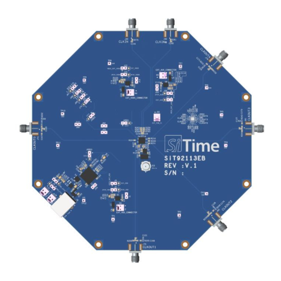
Page 14: Evb Snapshot
SiT92113 Ultra Low Jitter Buffer Evaluation Kit User Guide 12 EVB Snapshot Figure 10. EVB Snapshot Block 1 has jumper settings to configure chip VDD as mentioned in Table 5 Block 2 has jumper settings to configure chip VDDO as mentioned in Table 6. - Page 15 SiT92113 Ultra Low Jitter Buffer Evaluation Kit User Guide Table 7. Block 4 has jumpers to select Clock inputs (SEL) and to set OE as mentioned in Table 8 Block 5 has USB port to power up the board or to select jumper for power up using external supply as mentioned in Table 4.
-
Page 16: Pcb Schematic
SiT92113 Ultra Low Jitter Buffer Evaluation Kit User Guide 13 PCB Schematic 13.1. Schematic Sheet 1 Figure 11. Schematic Sheet 1 VDD (Input Side Supply) SiT92113EB User Manual | Rev 0.5 Page 16 of 24 www.sitime.com... -
Page 17: Schematic Sheet 2
SiT92113 Ultra Low Jitter Buffer Evaluation Kit User Guide 13.2. Schematic Sheet 2 Figure 12. Schematic Sheet 2 VDDO (Output Side Supply) SiT92113EB User Manual | Rev 0.5 Page 17 of 24 www.sitime.com... -
Page 18: Schematic Sheet 3
SiT92113 Ultra Low Jitter Buffer Evaluation Kit User Guide 13.3. Schematic Sheet 3 Figure 13. Schematic Sheet 3 Auxiliary Supply SiT92113EB User Manual | Rev 0.5 Page 18 of 24 www.sitime.com... -
Page 19: Schematic Sheet 4
SiT92113 Ultra Low Jitter Buffer Evaluation Kit User Guide 13.4. Schematic Sheet 4 Figure 14. Schematic Sheet 4 USB Connections SiT92113EB User Manual | Rev 0.5 Page 19 of 24 www.sitime.com... -
Page 20: Schematic Sheet 5
SiT92113 Ultra Low Jitter Buffer Evaluation Kit User Guide 13.5. Schematic Sheet 5 Figure 15. Schematic Sheet 5 FTDI Connections SiT92113EB User Manual | Rev 0.5 Page 20 of 24 www.sitime.com... -
Page 21: Schematic Sheet 6
SiT92113 Ultra Low Jitter Buffer Evaluation Kit User Guide 13.6. Schematic Sheet 6 Figure 16. Schematic Sheet 6 FTDI to DUT Mapping SiT92113EB User Manual | Rev 0.5 Page 21 of 24 www.sitime.com... -
Page 22: Schematic Sheet 7
SiT92113 Ultra Low Jitter Buffer Evaluation Kit User Guide 13.7. Schematic Sheet 7 Figure 17. Schematic Sheet 7 Input Clk0 SiT92113EB User Manual | Rev 0.5 Page 22 of 24 www.sitime.com... -
Page 23: Schematic Sheet 8
SiT92113 Ultra Low Jitter Buffer Evaluation Kit User Guide 13.8. Schematic Sheet 8 Figure 18. Schematic Sheet 8 DUT Connections SiT92113EB User Manual | Rev 0.5 Page 23 of 24 www.sitime.com... - Page 24 © SiTime Corporation February 2024. The information contained herein is subject to change at any time without notice. SiTime assumes no responsibility or liability for any loss, damage or defect of a Product which is caused in whole or in part by (i) use of any circuitry other than circuitry embodied in a SiTime product, (ii) misuse or abuse including static discharge, neglect or accident, (iii) unauthorized modification or repairs which have been soldered or altered during assembly and are not capable of being tested by SiTime under its normal test conditions, or (iv) improper installation, storage, handling, warehousing or transportation, or (v) being subjected to unusual physical, thermal, or electrical stress.
Need help?
Do you have a question about the SiT92113 and is the answer not in the manual?
Questions and answers