Advertisement
Quick Links
Table of Contents
1
Introduction ......................................................................................................................................................................... 2
2
Features .............................................................................................................................................................................. 2
3
Functional Description ......................................................................................................................................................... 3
3.1. VDD Power Supplies ............................................................................................................................................... 3
3.2. Output Enable .......................................................................................................................................................... 3
4
Power Supply Connections ................................................................................................................................................. 4
5
Setting Output Enable in the EVK ....................................................................................................................................... 5
6
Input Clock Configuration .................................................................................................................................................... 5
7
Configuring EVK for DC Coupled Input LVCMOS Clock ..................................................................................................... 6
7.1. Driving Clock Inputs with LVCMOS Driver (DC coupled) ......................................................................................... 6
8
PCB Schematic ................................................................................................................................................................... 7
8.1. Schematic Sheet1 .................................................................................................................................................... 7
8.2. Schematic Sheet2 .................................................................................................................................................... 8
8.3. Schematic Sheet3 .................................................................................................................................................... 9
SiT92184EB User Manual | Rev 0.5
SiT92184 Evaluation Board (EVB) HW
User Manual
Page 1 of 10
www.sitime.com
Advertisement

Subscribe to Our Youtube Channel
Related Manuals for SiTime SiT92184


Summary of Contents for SiTime SiT92184
- Page 1 SiT92184 Evaluation Board (EVB) HW User Manual Table of Contents Introduction ..................................2 Features ....................................2 Functional Description ................................. 3 3.1. VDD Power Supplies ............................... 3 3.2. Output Enable ................................3 Power Supply Connections ..............................4 Setting Output Enable in the EVK ............................5 Input Clock Configuration ..............................
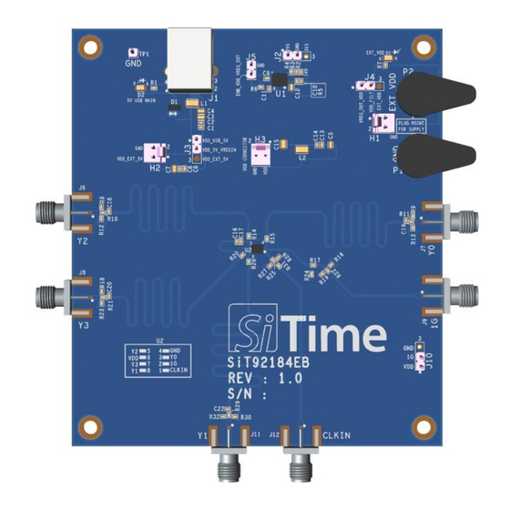
- Page 2 SiT92184 Evaluation Board (EVB) HW User Manual 1 Introduction The SiT92184 Evaluation Board is designed for evaluating the SiT92184, a high-performance LVCMOS ultra low jitter buffer. Figure 1. SiT92184 EVK Board 2 Features High-performance 1:4 LVCMOS clock buffer Very low pin-to-pin skew: <50 ps Very low additive jitter: <50 ps...
- Page 3 3 Functional Description The SiT92184 is a 4-output LVCMOS clock fan out buffer with low additive jitter that can operate up to 200MHz. The output buffer can be Enabled / Disabled via 1G pin. The device is offered in a 8-pin DFN (COL) package.
- Page 4 SiT92184 Evaluation Board (EVB) HW User Manual 4 Power Supply Connections SiT92184 buffer operates on a Single VDD supply. The VDD supply can be 3.3 V ±5%, 2.5 V ±5%, 1.8 V ±10%. The VDD supply can be set as in Table Table 2.
- Page 5 SiT92184 Evaluation Board (EVB) HW User Manual 5 Setting Output Enable in the EVK The jumper setting for controlling the output enable are given Table Table 4. Jumper settings to control clock select and output enable Jumper state Logic state...
- Page 6 SiT92184 Evaluation Board (EVB) HW User Manual 7 Configuring EVK for DC Coupled Input LVCMOS Clock 7.1. Driving Clock Inputs with LVCMOS Driver (DC coupled) Single ended clocks should be DC coupled to the CLKIN. This is shown Figure 4.
- Page 7 SiT92184 Evaluation Board (EVB) HW User Manual 8 PCB Schematic 8.1. Schematic Sheet1 Figure 5. Schematic Sheet 1 – DUT Connections SiT92184EB User Manual | Rev 0.5 Page 7 of 10 www.sitime.com...
- Page 8 SiT92184 Evaluation Board (EVB) HW User Manual 8.2. Schematic Sheet2 Figure 6. Schematic Sheet 2 – USB Connections SiT92184EB User Manual | Rev 0.5 Page 8 of 10 www.sitime.com...
- Page 9 SiT92184 Evaluation Board (EVB) HW User Manual 8.3. Schematic Sheet3 Figure 7. Schematic Sheet 3 – VDD Supply SiT92184EB User Manual | Rev 0.5 Page 9 of 10 www.sitime.com...
- Page 10 © Si ime Corporation February 2024. The information contained herein is subject to change at any time without notice. SiTime assumes no responsibility or liabili ty for any loss, damage or defect of a Product which is caused in whole or in part by (i) use of any circuitry other than circuitry embodied in a SiTime product, (ii) misuse or abuse including static discharge, neglect or accident, (iii) unauthorized modification or repairs which have been soldered or altered during assembly and are not capable of being tested by SiTime under its normal test conditions, or (iv) improper installation, storage, handling, warehousing or transportation, or (v) being subjected to unusual physical, thermal, or electrical stress.
Need help?
Do you have a question about the SiT92184 and is the answer not in the manual?
Questions and answers