Table of Contents
Advertisement
Quick Links
Table of Contents
1
Introduction ......................................................................................................................................................................... 1
2
Features .............................................................................................................................................................................. 1
3
Functional Description ......................................................................................................................................................... 2
3.1. VDD and VDDO Power Supplies ............................................................................................................................... 2
3.2. Clock Inputs ............................................................................................................................................................... 2
3.3. Clock States (Input vs Output States)........................................................................................................................ 1
3.4. Output Driver Type .................................................................................................................................................... 1
3.5. Reference Output ...................................................................................................................................................... 1
4
Power Supply Connections ................................................................................................................................................. 2
5
Setting Input Clock Select and REF Out Enable in the EVK ............................................................................................... 4
6
Input Clock Configuration .................................................................................................................................................... 5
7
Configuring for Single ended AC coupled Input Clock ........................................................................................................ 6
7.1. Driving Clock Inputs with LVCMOS Driver (AC coupled) ........................................................................................... 6
7.2. Driving Clock Inputs with LVCMOS Driver (DC coupled) ........................................................................................... 7
8
Driving Differential LVDS or LVDS Boost (AC coupled) ...................................................................................................... 9
8.1. Board Configuration for driving DC Coupled LVDS ................................................................................................... 9
9
Board Configuration Required for Driving DC/AC coupled LVPECL ................................................................................. 10
9.1. DC/AC Coupled LVPECL ........................................................................................................................................ 10
10
Output Configuration ......................................................................................................................................................... 11
11
EVB Snapshot ................................................................................................................................................................... 12
12
Schematics of SiT92216 Evaluation Kit ............................................................................................................................. 13
12.1. Schematic Sheet 1 ................................................................................................................................................ 13
12.2. Schematic Sheet 2 ................................................................................................................................................ 14
12.3. Schematic Sheet 3 ................................................................................................................................................ 15
12.4. Schematic Sheet 4 ................................................................................................................................................ 16
12.5. Schematic Sheet 5 ................................................................................................................................................ 17
12.6. Schematic Sheet 6 ................................................................................................................................................ 18
12.7. Schematic Sheet7 ................................................................................................................................................. 19
12.8. Schematic Sheet8 ................................................................................................................................................. 20
12.9. Schematic Sheet9 ................................................................................................................................................. 21
12.10. Schematic Sheet10 ............................................................................................................................................. 22
12.11. Schematic Sheet11 ............................................................................................................................................. 23
SiT92216EB User Manual | Rev 0.5
SiT92216 Evaluation Board (EVB) HW
User Manual
Page 1 of 27
www.sitime.com
Advertisement
Table of Contents

Related Manuals for SiTime SiT92216


Summary of Contents for SiTime SiT92216
-
Page 1: Table Of Contents
Board Configuration Required for Driving DC/AC coupled LVPECL ................. 10 9.1. DC/AC Coupled LVPECL ............................10 Output Configuration ................................. 11 EVB Snapshot ................................... 12 Schematics of SiT92216 Evaluation Kit ..........................13 12.1. Schematic Sheet 1 ..............................13 12.2. Schematic Sheet 2 ..............................14 12.3. Schematic Sheet 3 ..............................15 12.4. -
Page 2: Introduction
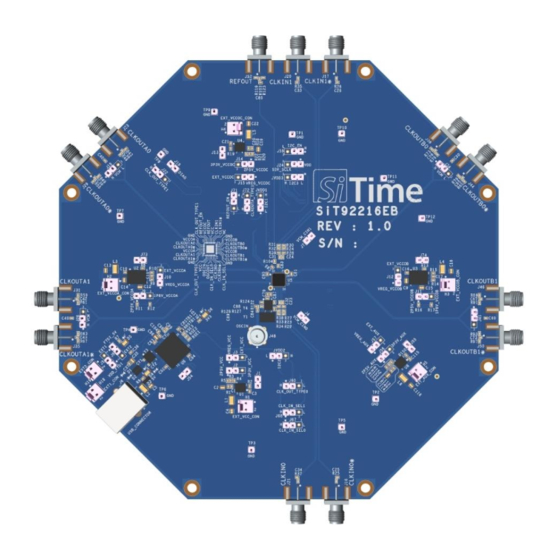
SiT92216 Evaluation Board (EVB) HW User Manual 1 Introduction The SiT92216 Evaluation Board is designed for evaluating the SiT92216, is a 4 differential output and 1 LVCMOS ultra low-jitter clock fan-out buffer. Figure 1. SiT92216 EVB Board 2 Features Additive jitter performance of 50 fs RMS. -
Page 3: Functional Description
3 Functional Description The SiT92216 is a 4 differential output and 1 LVCMOS output clock fan out buffer with low additive jitter that can operate up to 2.1 GHz. It features a 3:1 input multiplexer with an optional crystal oscillator input, two banks of 2 differential outputs with multi- mode buffers (LVPECL, LVDS, HCSL, or Hi-Z), one LVCMOS output, and 3 independent output buffer supplies. -
Page 4: Clock States (Input Vs Output States)
SiT92216 Evaluation Board (EVB) HW User Manual 3.3. Clock States (Input vs Output States) Table 2. Input versus Output Stages State of Selected Clock input Output State Inputs are floating Logic low Inputs are logic low logic low Inputs are logic high logic high 3.4. -
Page 5: Power Supply Connections
4 Power Supply Connections SiT92216 buffer has four suuplies VCC, VCCOA, VCCOB and VCCOC. The VCCOA supply is dedicated supply for the bank A output drivers. The VCCOA supply can be 3.3 V+/-5%, 2.5 V+/-5%, 1.8 V+/-5%. The VCCOB supply is dedicated supply for the bank B output drivers. - Page 6 SiT92216 Evaluation Board (EVB) HW User Manual Table 9. Setting VCCOC voltage Jumper setting VCCOC (V) J14 shorted between pins 2,3 J14 shorted between pins 1,2 J14 left open Note: Figure 16. Schematic Sheet 4 – VCCOC regulator 1. Refer for Jumper J11 connection.
-
Page 7: Setting Input Clock Select And Ref Out Enable In The Evk
SiT92216 Evaluation Board (EVB) HW User Manual 5 Setting Input Clock Select and REF Out Enable in the EVK The jumper setting for controlling the input clock select and output enable are given below. Table 11. Jumper settings to control clock select, ODR type change and REF out enable... -
Page 8: Input Clock Configuration
SiT92216 Evaluation Board (EVB) HW User Manual 6 Input Clock Configuration The input clock is ac coupled and terminated with differential 100 Ohms. Thus the EVK is configured for differential input clock as shown in schematic sheet9. The clock is ac coupled to the chip clock input pins. -
Page 9: Configuring For Single Ended Ac Coupled Input Clock
SiT92216 Evaluation Board (EVB) HW User Manual 7 Configuring for Single ended AC coupled Input Clock Many applications require the buffer to receive single ended input clock. Therefore, some minimal changes need to be done to the EVK to accomplish single ended operation. -
Page 10: Driving Clock Inputs With Lvcmos Driver (Dc Coupled)
Case1: Let us look at the case where a LVCMOS driver (of 50 Ohm impedance) drive a 50 Ohm load which is located at the input of SiT92216. Let the supply of LVCMOS driver be 1.8 V. Then the swing of the clock at the chip input is 0.9Vpp. We to set the reference voltage at the reference node at 0.45 V. - Page 11 SiT92216 Evaluation Board (EVB) HW User Manual Case2: If load is purely capacitive, let the supply of LVCMOS driver be 1.8 V. Then the swing of the clock at the chip input is 1.8 Vpp. We to set the reference voltage at the reference node at 0.9 V. Choose VCC = 1.8V, Rs2=Rs1. Rs1, Rs2 should be in the kilo ohm range.
-
Page 12: Driving Differential Lvds Or Lvds Boost (Ac Coupled)
SiT92216 Evaluation Board (EVB) HW User Manual 8 Driving Differential LVDS or LVDS Boost (AC coupled) The input sees a 100 Ohm differential resistance which gives a current path for LVDS or LVDS boost. The 100 Ohm differential signal is followed by AC coupling capacitor of 0.1 uF. So no change in board configuration is required. -
Page 13: Board Configuration Required For Driving Dc/Ac Coupled Lvpecl
SiT92216 Evaluation Board (EVB) HW User Manual 9 Board Configuration Required for Driving DC/AC coupled LVPECL 9.1. DC/AC Coupled LVPECL The LVPECL standard requires a DC path for the input clock driver. The 50 Ohm termination at the receiver is biased with VCCO-2 V. -
Page 14: Output Configuration
SiT92216 Evaluation Board (EVB) HW User Manual 10 Output Configuration The bank A and B outputs are by default configured for driving LVDS on the EVB. The bank A and B outputs are connected to the SMA output connectors via a differential transmission line and 0.1uF ac coupling capacitor. Appropriate differential 100 Ohm termination should be given for using LVDS configuration. -
Page 15: Evb Snapshot
SiT92216 Evaluation Board (EVB) HW User Manual 11 EVB Snapshot Figure 12. EVB Snapshot Block 1 has USB port to power up the board or to select jumper for power up using external supply as mentioned in Table Block 2 has jumper settings to configure chip VCC as mentioned in... -
Page 16: Schematics Of Sit92216 Evaluation Kit
SiT92216 Evaluation Board (EVB) HW User Manual 12 Schematics of SiT92216 Evaluation Kit 12.1. Schematic Sheet 1 Figure 13. Schematic Sheet 1 – VCC Regulator SiT92216EB User Manual | Rev 0.5 Page 13 of 27 www.sitime.com... -
Page 17: Schematic Sheet 2
SiT92216 Evaluation Board (EVB) HW User Manual 12.2. Schematic Sheet 2 Figure 14. Schematic Sheet 2 – VCCOA regulator SiT92216EB User Manual | Rev 0.5 Page 14 of 27 www.sitime.com... -
Page 18: Schematic Sheet 3
SiT92216 Evaluation Board (EVB) HW User Manual 12.3. Schematic Sheet 3 Figure 15. Schematic Sheet 3 – VCCOB regulator SiT92216EB User Manual | Rev 0.5 Page 15 of 27 www.sitime.com... -
Page 19: Schematic Sheet 4
SiT92216 Evaluation Board (EVB) HW User Manual 12.4. Schematic Sheet 4 Figure 16. Schematic Sheet 4 – VCCOC regulator SiT92216EB User Manual | Rev 0.5 Page 16 of 27 www.sitime.com... -
Page 20: Schematic Sheet 5
SiT92216 Evaluation Board (EVB) HW User Manual 12.5. Schematic Sheet 5 Figure 17. Schematic Sheet 5 – VDD_AUX regulator SiT92216EB User Manual | Rev 0.5 Page 17 of 27 www.sitime.com... -
Page 21: Schematic Sheet 6
SiT92216 Evaluation Board (EVB) HW User Manual 12.6. Schematic Sheet 6 Figure 18. Schematic Sheet 6 – Main supply from USB port SiT92216EB User Manual | Rev 0.5 Page 18 of 27 www.sitime.com... -
Page 22: Schematic Sheet7
SiT92216 Evaluation Board (EVB) HW User Manual 12.7. Schematic Sheet7 Figure 19. Schematic Sheet 7 – FTDI chip for automated control of GPIO pins SiT92216EB User Manual | Rev 0.5 Page 19 of 27 www.sitime.com... -
Page 23: Schematic Sheet8
SiT92216 Evaluation Board (EVB) HW User Manual 12.8. Schematic Sheet8 Figure 20. Schematic Sheet 8 – FTDI signal to DUT mapping SiT92216EB User Manual | Rev 0.5 Page 20 of 27 www.sitime.com... -
Page 24: Schematic Sheet9
SiT92216 Evaluation Board (EVB) HW User Manual 12.9. Schematic Sheet9 Figure 21. Schematic Sheet 9 – Input clock configuration SiT92216EB User Manual | Rev 0.5 Page 21 of 27 www.sitime.com... -
Page 25: Schematic Sheet10
SiT92216 Evaluation Board (EVB) HW User Manual 12.10.Schematic Sheet10 Figure 22. Schematic Sheet 10 – Output configuration- A and B Bank is configured as LVDS SiT92216EB User Manual | Rev 0.5 Page 22 of 27 www.sitime.com... -
Page 26: Schematic Sheet11
SiT92216 Evaluation Board (EVB) HW User Manual 12.11.Schematic Sheet11 Figure 23. Schematic Sheet 11 – SiT92216 Schematic Connections SiT92216EB User Manual | Rev 0.5 Page 23 of 27 www.sitime.com... - Page 27 © Si ime Corporation February 2024. The information contained herein is subject to change at any time without notice. SiTime assumes no responsibility or liabili ty for any loss, damage or defect of a Product which is caused in whole or in part by (i) use of any circuitry other than circuitry embodied in a SiTime product, (ii) misuse or abuse including static discharge, neglect or accident, (iii) unauthorized modification or repairs which have been soldered or altered during assembly and are not capable of being tested by SiTime under its normal test conditions, or (iv) improper installation, storage, handling, warehousing or transportation, or (v) being subjected to unusual physical, thermal, or electrical stress.
Need help?
Do you have a question about the SiT92216 and is the answer not in the manual?
Questions and answers