Table of Contents
Advertisement
Quick Links
Advertisement
Table of Contents

Related Manuals for Microchip Technology Microsemi PolarFire FPGA Evaluation Kit


Summary of Contents for Microchip Technology Microsemi PolarFire FPGA Evaluation Kit
- Page 1 UG0747 User Guide PolarFire FPGA Evaluation Kit Arrow.com. Downloaded from...
- Page 2 About Microsemi ©2021 Microsemi, a wholly owned Microsemi, a wholly owned subsidiary of Microchip Technology Inc. (Nasdaq: MCHP), offers a comprehensive portfolio of subsidiary of Microchip Technology Inc. All semiconductor and system solutions for aerospace & defense, communications, data center and industrial markets.
-
Page 3: Table Of Contents
Contents 1 Revision History ........... . . 1 Revision 5.0 . - Page 4 5 Pin List ............32 6 Board Component Placement .
- Page 5 Figures Figure 1 PolarFire Evaluation Kit Block Diagram ..........3 Figure 2 PolarFire Evaluation Board .
- Page 6 Tables Table 1 Kit Contents ..............2 Table 2 PolarFire Evaluation Board Components .
-
Page 7: Revision History
Revision History Revision History The revision history describes the changes that were implemented in the document. The changes are listed by revision, starting with the most current publication. Revision 5.0 Added Table 7, page 12 that lists the suggested power regulators. Revision 4.0 Added performance measurement data for different protocols, see Appendix 4: Performance Data,... -
Page 8: Getting Started
Getting Started Getting Started ® The Microsemi PolarFire FPGA Evaluation Kit (MPF300-EVAL-KIT), which is RoHS-compliant, enables you to evaluate the PolarFire family of FPGAs with support for the following interfaces: • PCI Express Gen1 and Gen2 • 1 GbE • DDR3 and DDR4 memory •... -
Page 9: Block Diagram
Getting Started Block Diagram The following block diagram shows all of the components of the PolarFire Evaluation Board. PolarFire Evaluation Kit Block Diagram Figure 1 • CON3 On Board SPI flash(1Gb) PCIe edge Oscillator- MT25QU01GBBB FMC HPC Connector connector 156.25 8ESF-0SIT HPC[HB0:21] HPC[HA0:23] LPC[0:33] 8 Lanes... -
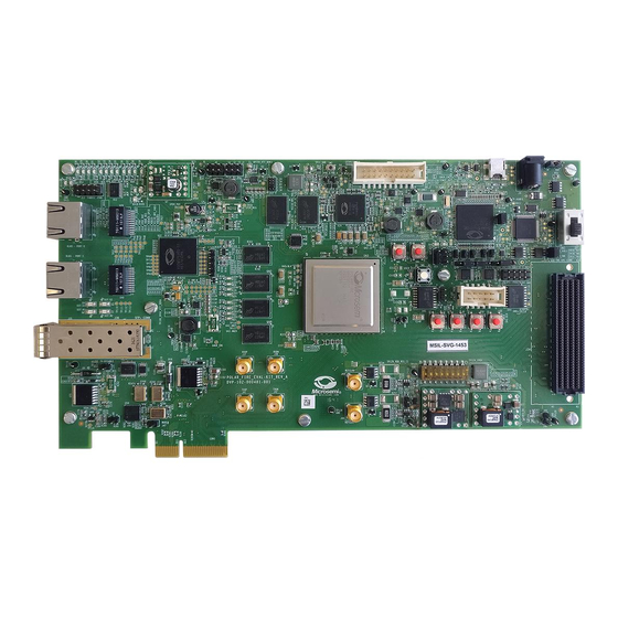
Page 10: Board Overview
Getting Started Board Overview The PolarFire Evaluation Board features the PolarFire MPF300TS-1FCG1152I FPGA. The device has the following capabilities: • 20 Kb dual-port or two-port large static random access memory (LSRAM) block with a built-in single error correct double error detect (SECDED) •... -
Page 11: Table 2 Polarfire Evaluation Board Components
Getting Started The following table lists the important components of the PolarFire Evaluation Board: PolarFire Evaluation Board Components Table 2 • Component Label on Board Description Featured Device PolarFire FPGA MPF300TS-1FCG1152I FPGA with data security feature Power Supply and Monitoring 12 V power supply The board is powered by a 12 V power source using an input... - Page 12 Getting Started Table 2 • PolarFire Evaluation Board Components (continued) Component Label on Board Description x4 PCIe edge PCIe edge connector with four lanes connector Tx/Rx XCVR2 SMA XCVR0 TXD0P pairs XCVR0 TXD0N XCVR0 RXD0P XCVR0 RXD0N Two 10/100/1000 J15 and J30 Ethernet (RJ45) jacks with external magnetics interfacing Ethernet RJ45 with Microsemi quad 10/100/1000 BASE-T PHY chip and...
-
Page 13: Compatibility With Daughter Boards
Getting Started Compatibility With Daughter Boards Daughter boards with FMC connectors can be plugged into the PolarFire Evaluation board. Handling the Board Pay attention to the following points while handling or operating the board to avoid possible damage or malfunction: •... -
Page 14: Installation And Settings
Installation and Settings Installation and Settings This section provides information about the software and hardware settings required to run the pre-programmed demo design on the PolarFire Evaluation Board. Software Settings ® Download and install the latest release of Microsemi Libero SoC PolarFire from the Microsemi website, and register for a free one-year Libero Gold software license. -
Page 15: Leds
Installation and Settings Table 3 • Jumper Settings (continued) Jumper Description Default Setting Jumper to Close pin 1 and 2 for programming through the External Open select between SPI flash FTDI SPI or External SPI Flash to program the device Jumper to Close pin 1 and 2 to define the SPI Slave mode Open... -
Page 16: Test Points
Installation and Settings Table 4 • LEDs (continued) Description DS13- Green VCCIO_HPC_VADJ voltage DS14 - Green VDDAUX Voltage rail DS18 - Green 12 V voltage rail DS16 - Green 5 V voltage rail DS17 - Green 3.3 V voltage rail 3.2.3 Test Points The following table lists USB, ground, and other test points. -
Page 17: Power Sources
Installation and Settings Power Sources The PolarFire Evaluation Board uses Microsemi power supply devices. For more information about power supply devices, see www.microsemi.com/product-directory/ics/853- power-management. The following table lists the key power supplies required for normal operation of the PolarFire Evaluation Board. -
Page 18: Figure 3 Voltage Rails In Polarfire Evaluation Board
Installation and Settings Figure 3 • Voltage Rails in PolarFire Evaluation Board 12V DC - JACK 12VO_IN VDD25/VDDA25/ IRF_12V VDD_XCVR_CLK Switching PMOS Switch PMOS Switch Linear Regulator 2.5 V Regulator Gate Gate Gate Bank Supply switching 1.2/2.5/1.8/1.5/1.2 V Regulator VDD18/Bank Supply 1.8 V Switching Main ON/OFF... - Page 19 Installation and Settings Table 7 • Power Regulators (continued) Voltage rail Part Number Description Current VDD25, VDDA25, MIC69502WR IC REG LINEAR POS ADJ 5A SPAK-7 VDD_XCVR_CLK VDD18 MIC69502WR IC REG LINEAR POS ADJ 5A SPAK-7 These regulators are not pin compatible with the existing evaluation kit schematics. Use these regulators for new board designs.
-
Page 20: Board Components And Operations
Board Components and Operations Board Components and Operations This section describes the key components of the PolarFire Evaluation board and important board operations. For device datasheets, visit www.microsemi.com/products/fpga-soc/design-resources/dev- kits/polarfire-kits. Memory Interface GPIO and HSIO bank I/Os for DDR3 and DDR4 are available in the PolarFire device. In addition to dedicated I/Os, regular I/Os can also be used to connect to other memory devices. -
Page 21: Spi Serial Flash
Board Components and Operations Figure 5 • DDR4 Memory Interface DDR4 Chips PolarFire Data DQ[31:0] DQS/DQS#[3:0] DDR4 SDRAM HSIO-BANK0,7 1G×8 (1 GB) 4 memory chips Address A[15:0] Control lines For more information, see the Board Level Schematics document (provided separately). SPI Serial Flash The SPI flash specifications for the PolarFire device are: •... -
Page 22: Xcvr1 And Xcvr3 Interface
Board Components and Operations The following figure shows the XCVR0 interface of the PolarFire Evaluation Board. XCVR0 Interface Figure 7 • PolarFire Lane0/ RXD Lane1/ RXD Lane2/ RXD Lane3/ RXD PCIe Edge connector Lane0/ TXD Lane1/ TXD Lane2/ TXD Lane3/ TXD REFCLK0 For information about PCI Express support in PolarFire, see UG0685: PolarFire FPGA PCI Express User... -
Page 23: Figure 8 Xcvr1 And Xcvr3 Interface
Board Components and Operations The following figure shows the XCVR1 and 3 interface of the PolarFire Evaluation Board. XCVR1 and XCVR3 Interface Figure 8 • PolarFire XCVR1 Lane0/ RXD XCVR1 Lane1/ RXD XCVR1 Lane2/ RXD XCVR1 Lane3/ RXD XCVR3 Lane0/ RXD XCVR3 Lane1/ RXD XCVR3 Lane2/ RXD XCVR3 Lane3/ RXD... -
Page 24: Xcvr2 Interface
Board Components and Operations 4.3.3 XCVR2 Interface The XCVR2 interface has four lanes connected as follows: • Lane 0 is connected to SMA connectors. • TX pad > trace > AC coupling > trace > SMA connectors (J41 (P) and J42 (N)) •... -
Page 25: Microsemi Phy (Vsc8575)
Board Components and Operations The following figure shows the XCVR reference clocks are interface of the PolarFire Evaluation Board. Figure 10 • XCVR Reference Clocks PolarFire FMC-HPC-CLK XCVR1B - REFCLK 156.25 MHz 156.25 XCVR2C - REFCLK MHz Clock FMC-HPC-CLK XCVR1C - REFCLK FMC-HPC-CLK XCVR3C - REFCLK XCVR2B - REFCLK... -
Page 26: Microsemi 1588V2 (Zl30364Gdg2)
Board Components and Operations 4.4.1 Microsemi 1588v2 (ZL30364GDG2) The PolarFire Evaluation Board uses Microsemi ZL30364GDG2 to provide the 125 MHz clock and reserved clocks to VSC8575 PHY. Device ZL30364GDG2 is configurable through the SPI interface and connected to the PolarFire device. The ZL30364GDG2 clock outputs are LVPECL and LVCMOS. Key features of Microsemi PHY ZL30364GDG2 are as follows: •... -
Page 27: Programming
Board Components and Operations The following figure shows the Microsemi PolarFire Power measurement system on the PolarFire Evaluation Board. Figure 12 • Power Management PolarFire Power Management Schematic VDD25/VDDA25_MON_SIG 12V Input PMOS PMOS Jack 12V to 5V/6A PTH08T231WAZ VDD_IN 12V Enable Power VDD25/5A Switch... -
Page 28: System Reset
Board Components and Operations The following figure shows the FTDI interface of the PolarFire Evaluation Board. Figure 13 • FTDI Interface PolarFire HSIO Bank6 UART JTAG SIGNALS Header JTAG JTAG Bank3 SIGNALS Jumper J18,19,20,21,22 USB mini B Port A FT4232 connector External J28 Jumper... -
Page 29: User Leds
Board Components and Operations 4.9.1 User LEDs The board has eight active-High LEDs that are connected to the PolarFire device. The following table lists the on-board user LEDs. Table 8 • User LEDs PolarFire PolarFire FPGA Evaluation Board Pin Number PolarFire FPGA Pin Name Bank LED7... -
Page 30: Slide Switches (Dpdt)
Board Components and Operations The following figure shows the switches interface of the PolarFire Evaluation Board. Figure 16 • Switches Interface 1.8 V PolarFire SW10 4.9.3 Slide Switches (DPDT) The SW3 slide switch powers the device ON or OFF from +12 V external DC jack. 4.9.4 DIP Switches (SPST) The SW11 DIP switch has eight connections to the PolarFire device. -
Page 31: Fmc Hpc Connector
Board Components and Operations The following figure shows the SPST interface on the PolarFire Evaluation Board. Figure 17 • SPST Interface 1.8 V SW11 DIP1 DIP2 DIP3 DIP4 PolarFire DIP5 DIP6 DIP7 DIP8 For more information, see the Board-Level Schematics document (provided separately). 4.9.5 FMC HPC Connector The PolarFire Evaluation Board has one HPC (J34) FMC connector for the daughter cards for future... -
Page 32: Table 11 J34 Fmc Connector Pinout
Board Components and Operations Table 11 • J34 FMC Connector Pinout (continued) FMC Pin PolarFire Pin Number-J34 FMC Net Name Number PolarFire Pin Name HPC_SERDES_3_RX1_P XCVR_3_RX1_P HPC_SERDES_3_RX1_N XCVR_3_RX1_N HPC_SERDES_1_TX1_P XCVR_1_TX1_P HPC_SERDES_1_TX1_N XCVR_1_TX1_N HPC_SERDES_1_TX2_P XCVR_1_TX2_P HPC_SERDES_1_TX2_N XCVR_1_TX2_N HPC_SERDES_1_TX3_P XCVR_1_TX3_P HPC_SERDES_1_TX3_N XCVR_1_TX3_N HPC_SERDES_3_TX0_P XCVR_3_TX0_P HPC_SERDES_3_TX0_N... - Page 33 Board Components and Operations Table 11 • J34 FMC Connector Pinout (continued) FMC Pin PolarFire Pin Number-J34 FMC Net Name Number PolarFire Pin Name HPC_LA14_P_B2 GPIO22PB2 HPC_LA14_N_B2 GPIO22NB2 HPC_LA18_CC_P_B2 GPIO11PB2/CLKIN_S_7 HPC_LA18_CC_N_B2 GPIO11NB2 HPC_LA27_P_B2 GPIO13PB2 HPC_LA27_N_B2 GPIO13NB2 HPC_SCL_B4 GPIO205PB4/DQS HPC_SDA_B4 GPIO205NB4/DQS HPC_SERDES_1_INT_REFCLK_P XCVR_1A_REFCLK_P HPC_SERDES_1_INT_REFCLK_N...
- Page 34 Board Components and Operations Table 11 • J34 FMC Connector Pinout (continued) FMC Pin PolarFire Pin Number-J34 FMC Net Name Number PolarFire Pin Name HPC_HA16_P_B4 GPIO199PB4/DQS HPC_HA16_N_B4 GPIO199NB4/DQS HPC_HA20_P_B4 GPIO197PB4 HPC_HA20_N_B4 GPIO197NB4 HPC_HB03_P_B5 GPIO235PB5/DQS HPC_HB03_N_B5 GPIO235NB5/DQS HPC_HB05_P_B5 GPIO236PB5 HPC_HB05_N_B5 GPIO236NB5 HPC_HB09_P_B5 GPIO237PB5 HPC_HB09_N_B5...
- Page 35 Board Components and Operations Table 11 • J34 FMC Connector Pinout (continued) FMC Pin PolarFire Pin Number-J34 FMC Net Name Number PolarFire Pin Name HPC_HB16_P_B5 GPIO232PB5 HPC_HB16_N_B5 GPIO232NB5 HPC_HB20_P_B5 GPIO228PB5 HPC_HB20_N_B5 GPIO228NB5 HPC_CLK1_M2C_P_B2 GPIO29PB2/CLKIN_S_9/CC C_SE_CLKIN_S_9 HPC_CLK1_M2C_N_B2 GPIO29NB2 HPC_LA00_CC_P_B2 GPIO7PB2/CLKIN_S_5 HPC_LA00_CC_N_B2 GPIO7NB2 HPC_LA03_P_B2 GPIO32PB2/DQS...
- Page 36 Board Components and Operations Table 11 • J34 FMC Connector Pinout (continued) FMC Pin PolarFire Pin Number-J34 FMC Net Name Number PolarFire Pin Name HPC_LA07_P_B2 GPIO0PB2 HPC_LA07_N_B2 GPIO0NB2 HPC_LA11_P_B2 GPIO35PB2/CCC_SE_CLKI N_S_11 HPC_LA11_N_B2 GPIO35NB2 HPC_LA15_P_B2 GPIO16PB2 HPC_LA15_N_B2 GPIO16NB2 HPC_LA19_P_B2 GPIO17PB2 HPC_LA19_N_B2 GPIO17NB2 HPC_LA21_P_B2 GPIO1PB2...
- Page 37 Board Components and Operations Table 11 • J34 FMC Connector Pinout (continued) FMC Pin PolarFire Pin Number-J34 FMC Net Name Number PolarFire Pin Name HPC_HB07_P_B5 GPIO233PB5 HPC_HB07_P_B5 GPIO233NB5 HPC_HB11_P_B5 GPIO220PB5 HPC_HB11_N_B5 GPIO220NB5 HPC_HB15_P_B5 GPIO222PB5 HPC_HB15_N_B5 GPIO222NB5 HPC_HB18_P_B5 GPIO226PB5 HPC_HB18_N_B5 GPIO226NB5 HPC_CLK2_BIDIR_P_B4 GPIO174PB4/CLKIN_W_7/C CC_NW_CLKIN_W_7/CCC_...
-
Page 38: Pin List
Pin List Pin List For information on all of the package pins on the PolarFire device, see Package Pin Assignment Table. Microsemi Proprietary UG0747 Revision 5.0 Arrow.com. Downloaded from... -
Page 39: Board Component Placement
Board Component Placement Board Component Placement The following figure shows the placement of various components on the PolarFire Evaluation Board silkscreen. Figure 18 • Silkscreen Top View TP11_GND TP-AGND1 TRST 3P3V_SF DS24 C4 D3 D4 1.2V TP-GND1 DS23 R56 R57 1.5V 3P3V TRST R348... -
Page 40: Appendix 1: Running The Demo Design
Appendix 1: Running the Demo Design Appendix 1: Running the Demo Design The onboard PolarFire FPGA comes with a programmed design. For more information on running the demo, see DG0755: PolarFire FPGA JESD204B Standalone Interface. Microsemi Proprietary UG0747 Revision 5.0 Arrow.com. -
Page 41: Appendix 2: Programming Polarfire Fpga Using The On-Board Flashpro5
Appendix 2: Programming PolarFire FPGA Using the On-Board FlashPro5 Appendix 2: Programming PolarFire FPGA Using the On-Board FlashPro5 The PolarFire Evaluation Board includes onboard FlashPro5 programmer hardware. An external programmer hardware is therefore not required to program the PolarFire device. The device can be programmed using the FlashPro software installed on the host PC. -
Page 42: Appendix 3: Power Monitoring
Appendix 3: Power Monitoring Appendix 3: Power Monitoring The SmartFusion A2F 200 device on the PolarFire Evaluation Board, monitors the voltage and current on different PolarFire power rails. It measures the current for different components and displays the power on the Microsemi PowerMonitor application. PowerMonitor is a Graphical User Interface (GUI) application that runs on the host PC. -
Page 43: Installing Powermonitor
Appendix 3: Power Monitoring Installing PowerMonitor To install PowerMonitor: Extract the contents of the polarfire_power_monitor.rar file. From POWER_MONITOR_GUI\Installer folder, double-click the setup.exe file. Follow the instructions displayed on the installation wizard. After successful installation, PowerMonitor appears on the Start menu of the host PC desktop. From the Start menu, click PowerMonitor. - Page 44 Appendix 3: Power Monitoring Note: For more information about the recommended minimum and maximum operating voltage of each rail, see the “Recommended Operating Conditions” section of DS0141: PolarFire FPGA Datasheet. The PowerMonitor GUI has the following buttons: • Graph—Click this button to view the power consumed by VDD_REG, VDDA_REG, VDDA25, and VDD25_DUT rails, and the total device power.
-
Page 45: Appendix 4: Performance Data
Appendix 4: Performance Data Appendix 4: Performance Data This section describes the performance results of MPF300T Evaluation Kit with different SERDES protocols. All of the steps required to set up the test environment are described. The section also provides information about eye diagram and jitter, and how they vary with protocol. All the measurements are taken on MPF300T Evaluation Kit with 23 GHz Tektronix scope. -
Page 46: Jesd204B Results
Appendix 4: Performance Data 10.2 JESD204B Results The following driver settings are used for JESD measurements: • Signal amplitude: 500 mV • De-emphasis: 0 dB • Pattern used: JSPAT (500 bits) • Driver Impedance: 100 Ω • Data Rate: 12.5 Gbps The following table summarizes the measurements captured by the scope at 12.5 Gbps transmitter data rate and at a BER of 10E-12. -
Page 47: 10Base-G Kr
Appendix 4: Performance Data 10.3 10BASE-G KR The following driver settings are used for 10BASE-G KR measurements: • Signal amplitude: 1000 mV • De-emphasis: -1 dB • Pattern used: PRBS31 • Driver impedance: 180 Ω • Data rate: 10.3125 Gbps The following table summarizes the measurements captured by the scope at 10.3125 Gbps transmitter data rate and at a BER of 10E-12. -
Page 48: Interlaken
Appendix 4: Performance Data 10.4 Interlaken The following driver settings are used for Interlaken measurements: • Signal amplitude: 500 mV • De-emphasis: 0 dB • Pattern used: PRBS31 • Driver impedance: 100 Ω • Data rate: 10.3125 Gbps The following table summarizes the measurements captured by the scope at of 10.3125 Gbps transmitter data rate and at a BER of 10E-12. -
Page 49: Cpri
Appendix 4: Performance Data 10.5 CPRI The following driver settings are used for CPRI measurements: • Signal amplitude: 1000 mV • De-emphasis: -1 dB • Pattern used: PRBS31 • Driver Impedance: 180Ω • Data Rate: 10.137 Gbps The following table summarizes the measurements captured by the scope at 10.137 Gbps transmitter data rate and at a BER of 10E-12. -
Page 50: Appendix 5: Errata
Appendix 5: Errata Appendix 5: Errata This section contains information about known issues specific to the PolarFire Evaluation Board. 11.1 Errata Descriptions 11.1.1 Hot swapping is not supported on Programming headers J32, J29, PCIe CONN (CON3), SFP+ cage (J36), GPIO headers (J7, J8) This restriction applies to Rev B and C of the board.
Need help?
Do you have a question about the Microsemi PolarFire FPGA Evaluation Kit and is the answer not in the manual?
Questions and answers