Advantech AIWireless AIW-356 DQ-JK1 User Manual
Hide thumbs
Also See for AIWireless AIW-356 DQ-JK1:
- User manual (65 pages) ,
- User manual (66 pages) ,
- User manual (58 pages)
Advertisement
Quick Links
Advertisement

Related Manuals for Advantech AIWireless AIW-356 DQ-JK1


Summary of Contents for Advantech AIWireless AIW-356 DQ-JK1
- Page 1 AIW-356 DQ-JK1 User Manual...
- Page 2 Applicability Type AIW PN Description 5G communication module with M.2 interface for AIW-356 DQ-JK1 FM160-JK-01 Japan and South Korea, USB only for data transmission...
- Page 3 Revision History Version Date Description First issue V1.0.0 2023-04-6 Change file name from Datasheet to User Manual V1.0.1 2023-05-30 Modify section 3.1 & 4.1.4 & 4.4.2 V1.0.2 2023-06-08...
- Page 4 1 Foreword 1.1 Introduction The document describes the electrical characteristics, RF performance, dimensions and application environment, etc. of AIW-356 DQ-JK1 (hereinafter referred to as AIW-356). With the assistance of the document and other instructions, the developers can quickly understand the hardware functions of AIW-356 DQ-JK1 modules and develop products.
- Page 5 Overview 2.1 Introduction AIW-356 DQ-JK1 is a highly integrated 5G wireless communication module which uses M.2 form factor interface. It supports 5G NR SUB6/LTE FDD/LTE TDD/WCDMA systems and can be applied to most cellular networks of mobile operators in the world. 2.2 Specifications 2.2.1.
- Page 6 Mode AIW-356 DQ-JK1 Support max DL 5CA Support max UL 2CA Support 3GPP R16 Support DL 256-QAM, UL 256-QAM Support RF bandwidth 1.4MHz–20MHz Support max DL LTE 5CA + NR 1CA Support max DL LTE 3CA + NR 2CA Support max UL LTE 1CA + NR 1CA LTE Modulation: DL-256QAM, UL-256QAM NR Modulation: DL-256QAM, UL-256QAM Support max DL 2CA...
- Page 7 2.2.2. Product Specification Mode AIW-356 DQ-JK1 Specification Qualcomm SDX62, 7nm process, ARM Cortex-A7, up to 1.5 GHz Memory 4Gb LPDDRX4+4Gb NAND Flash Supported OS Linux / Android / Windows Class 3 (23.5dBm±1.5dB) for LTE, 20dBm±1.5dB for LTE B39 Power Level Class 3 (23dBm±1.5dB) for NR Sub6 bands Class 2 (26dBm±1.5dB) for n78 bands DC 3.135V to 4.4V, Typical 3.8V...
- Page 8 Interface Function Interface Antenna tuner interface Software Protocol Stack IPV4/IPV6 AT commands 3GPP TS 27.007 and 27.005 Firmware update Multiple Carrier Other features AGNSS Table 2-4 Product Specification Note: When temperature goes beyond normal operating temperature range, RF performance of module may all out of the 3GPP specifications.
- Page 9 2.3 Application Framework The peripheral applications for AIW-356 DQ-JK1 module are shown in Figure 2-1: Figure 2-1 Application framework...
- Page 10 2.4 Hardware Block Diagram The hardware block diagram in Figure 2-2 shows the main hardware functions of AIW-356 DQ-JK1 module, including baseband and RF functions. Baseband functions contain: UMTS/LTE/NR Controller NAND/LPDDR RAM Application Interface RF functions contain: ...
- Page 11 Figure 2-2 Hardware block diagram...
- Page 12 2.5 Antenna Configuration AIW-356 DQ-JK1 module supports four antennas and the configuration is shown in the following table: Band Configuration Frequenc Antenna Function Band Configuration (RX) Range Connector Description (TX) (MHz) Main ANT/ LTE: B1/3/7/39/41/42 LTE: B1/3/7/39/41/42 617-960 ANT0 1427-2690 3300-5000 NR: n1/3/7/41/77/78/79 NR: n1/3/7/41/77/78/79...
- Page 13 Application Interfaces 3.1. M.2 Key-B Interfaces 3.1.1. Pin Map Pin No. AIW-356 DQ-JK1 Pin No. CONFIG_2 FORCE_USB_BOOT(1.8V) CONFIG_1 SIM Detect (1.8V) RESET#(3.3V/1.8V) COEX1 (1.8V) ANTCTL3 (1.8V) COEX2 (1.8V) ANTCTL2 (1.8V) WLAN_TX_EN(1.8V) ANTCTL1 (1.8V) RFFE_SDATA(1.8V) LAA_TX_EN(1.8V) RFFE_SCLK(1.8V) PEWAKE# (3.3/1.8V) REFCLKP CLKREQ# (3.3/1.8V) REFCLKN PERST# (3.3/1.8V) UIM2_PWR...
- Page 14 Pin No. AIW-356 DQ-JK1 Pin No. I2S_WA (1.8V) USB_SS-TX- W_DISABLE2#(3.3/1.8V) I2S_TX (1.8V) DPR(3.3/1.8V) I2S_RX (1.8V) WOWWAN# (1.8V) I2S_CLK (1.8V) CONFIG_0 Notch Notch Notch Notch Notch Notch Notch Notch LED1#(OD) W_DISABLE1#(3.3/1.8V) USB_D- FULL_CARD_POWER_OFF# USB_D+ CONFIG_3 (NC) Figure 3-1 Pin map Note: The AIW-356 DQ-JK1 module applies standard M.2 Key-B interface, with a total of 75 pins.
- Page 15 3.1.2. Pin Definition Reset Pin Pin Name Description Type Value NC, AIW-356 DQ-JK1 M.2 module is configured as the WWAN – PCIe CONFIG_3 with the USB_SS interface type Power Power input Supply Power Supply Power Power input Supply Power Supply Module power-on/off control, the module is powered off when the pin is FULL_CARD_...
- Page 16 Reset Pin Pin Name Description Type Value Notch Notch Notch Notch I2S_CLK I2S Serial clock 1.8V NC, AIW-356 DQ-JK1 M.2 module is configured as the WWAN – PCIe CONFIG_0 with the USB_SS interface type I2S_RX I2S Serial receive data 1.8V WOWWAN# Wake up host 1.8V...
- Page 17 Reset Pin Pin Name Description Type Value Negative end of USB super USB_SS-RX - speed data receiving 1.8V/ UIM1_PWR SIM card 1 power supply, 3V/1.8V USB_SS-RX+ USB super speed receive data plus 1.8V Power Supply SIM card 2 detection, internally pulled up through 390KΩ...
- Page 18 Reset Pin Name Description Type Value Device requests a PCIe reference clock to transmit data. It is also used by L1 power management 3.3V/ CLKREQ# status mechanism. Host or device 1.8V initiates an L1 exit. Active low, An external pull-up resistor must be reserved.
- Page 19 Reset Pin Pin Name Description Type Value A high level on this pin disables n79 LNAs. Normally this signal is WLAN_TX_EN from external 5 GHz WLAN when its transmitting power exceeds a threshold. ANTCTL1 Tunable antenna control bit 1 1.8V BT-SIG based module public network RF and WiFi/BT wireless COEX_2...
- Page 20 Reset Pin Pin Name Description Type Value Module reset, pulled up through 3.3V/ RESET# 1.8V 390KΩ internal resistor, active low After the pin is pulled up to 1.8V during power-on, the module will enter the USB download mode. The pin is used for FORCE_USB_BOOT I updating the software of module 1.8V...
- Page 21 Reset Value: The initial status after module reset, not the status when working. H: High Level L: Low Level PD: Pull-Down PU: Pull-Up T: Tri-state, high resistance OD: Open Drain PI: Power Input PO: Power Output Note: The unused pins can be left floating. All interfaces that support 3.3V voltage are based on the input voltage of +3.3V power supply.
- Page 22 3.2. Power Supply DC Parameter (V) Pin Name Pin Description Minimum Typical Maximum Value Value Value 2, 4, 70, 72, 74 VCC Power supply input 3.135 UIM1_PWR PO USIM power supply 1.8V/3V UIM2_PWR PO USIM power supply 1.8V/3V Table 3-2 AIW-356 DQ-JK1 module power interface 3.2.1.
- Page 23 Recommended Application Description Capacitance To reduce power fluctuations of the module in operation, use low-ESR capacitors. For LDO or DC/DC power supply, the 220uF x 2 Voltage regulating capacitors capacitance should be no less than 440uF. For battery power supply, the capacitance can be reduced to 100 uF to 200uF.
- Page 24 3.2.2. Logic Level Parameter Minimum Typical Maximum Unit 1.8V logic level 1.71 1.89 -0.3 Table 3-4 Definition of 1.8V logic level Parameter Minimum Typical Maximum Unit 3.3V logic level 3.135 3.465 3.465 -0.3 Table 3-5 Definition of 3.3V logic level 3.2.3.
- Page 25 Typical State Mode Condition Current/mA I off Power off Power supply, module power-off 0.18 TDD LTE DPC (Default Paging Cycle) =#128 FDD LTE DPC (Default Paging Cycle) =#128 (USB IDLE Disconnection.) Long DRX (ms10) Radio Off AT+CFUN=4 Flight Mode TDD LTE DPC (Default Paging Cycle) =#128 FDD LTE DPC (Default Paging Cycle) =#128...
- Page 26 Typical State Mode Condition Current/mA n1@max power @23dBm (10MHz, Inner full RB) n3@max power @23dBm (10MHz, Inner full RB) SA FDD n7@max power @23dBm (10MHz, Inner full RB) n8@max power @23dBm (10MHz, Inner full RB) n28@max power @23dBm (10MHz, Inner full RB) n41@max power @23dBm (100MHz, Inner full RB) 470 n77@max power @23dBm (100MHz, Inner full RB) 465 SA TDD...
- Page 27 3.3. Control Signals The AIW-356 DQ-JK1 module provides two control signals for power-on/off and reset operations, the pins are defined in the following table: Reset Pin Pin Name Description Type Value Module power-on/off control Pulled up through internal 3.3V/ 470KΩ resistor FULL_CARD_POWER_OFF# 1.8V Power-on: High/Floating...
- Page 28 3.3.1. Module Power-on 3.3.1.1. Power-on Circuit When the FCPO# (FULL_CARD_POWER_OFF#) pin and reset (RESET#) pin are floating or connect to an external 3.3V/1.8V, the module will boot up. When AP (Application Processor) controls the module start-up, it is recommended that the FULL_CARD_POWER_OFF# and RESET# GPIO port should use a port with low level for reset or internal pull down and the external pull-down resistance should be reserved.
- Page 29 Index Min. Recommended Max. Remarks Delay time of FCPO# relative to power ready(3.135V) t pr Delay time of RESET# signal relative to FCPO# t on1 signal Delay time of PERST# signal relative to FCPO# signal, PERST# must always be the last signal to pull t on2 50ms 100ms...
- Page 30 Figure 3-6 Recommended power-off timing Index Min. Recommended Max. Comment Pull-down delay time of RESET# signal relative to 16ms 20ms off1 PERST# signal Pull-down delay time of FCPO# signal relative to t on1 RESET# signal +3.8V power supply off delay time. If power supply is t pd 10ms 100ms...
- Page 31 3.3.3. Module Reset The AIW-356 DQ-JK1 module can reset to its initial status by pulling down the RESET# signal for more than 30ms (50ms is recommended), and module will restart after RESET# signal is released. The recommended circuit design is shown in the Figure 3-7: Figure 3-7 Recommended design for reset circuit There are two reset control timings as below: Reset timing 1 st in Figure 3-8.
- Page 32 Figure 3-9 Reset timing 2 Index Min. Recommended Max. Remarks Pull-down delay time of RESET# signal relative to PERST#. 16ms 20ms off1 For details, refer to section 3.3.2 Pull-down delay time of FCPO# signal relative to RESET#. off2 For details, refer to section 3.3.2 Power-off time must be not less than 500ms to ensure the 500ms...
- Page 33 3.4. USB Interfaces AIW-356 DQ-JK1 module supports USB2.0 and is compatible with USB High-Speed (480 Mbit/s) and USB Full-Speed (12 Mbit/s). At the same time, AIW-356 DQ-JK1 also supports USB_3.1 Gen2 10Gbit/s to achieve ultra-high-speed data transmission, which is used to meet the high-speed transmission requirements of 5G mobile networks.
- Page 34 3.4.2. USB2.0 Interface Application The reference circuit is shown in Figure 3-10: Figure 3-10 Reference circuit for USB 2.0 interface USB_D- and USB_D+ are high speed differential signal lines with the maximum transfer rate of 480 Mbit/s. The following rules shall be followed carefully in the case of PCB layout: USB_D- and USB_D+ signal lines should have the differential impedance of 90±10Ω.
- Page 35 3.4.3. USB3.1 Interface Application The reference circuit is shown in Figure 3-11: Figure 3-11 Reference circuit for USB 3.1 interface USB 3.1 Gen2 signals are super speed differential signal lines with the maximum transfer rate of 10Gbps. The following rules shall be followed carefully in the case of PCB layout: ...
- Page 36 3.5.1. USIM1 Pins The USIM1 pins are listed in the following table: Pin Name Reset Value Description Type UIM1_PWR USIM1 power supply 1.8V/3V UIM1_RESET USIM1 reset 1.8V/3V UIM1_CLK USIM1 clock 1.8V/3V USIM1 data, internally pulled up UIM1_DATA 1.8V/3V (20KΩ) USIM1 card detection, internally pulled up (390KΩ).
- Page 37 3.5.3. USIM Interface Circuit 3.5.3.1. N.C. SIM Card Slot The reference circuit design for N.C. (Normally Closed) SIM card slot is shown in Figure 3-12: Figure 3-12 Reference circuit for N.C. SIM card slot The principles of the N.C.SIM card slot are described as follows: ...
- Page 38 3.5.3.2. N.O. SIM Card Slot The reference circuit design for N.O. (Normally Open) SIM card slot is shown in Figure 3-13: Figure 3-13 Reference circuit for N.O. SIM card slot The principles of the N.O.SIM card slot are described as follows: ...
- Page 39 AT Command Hot-plug Detection Function Description By default, the SIM card hot plug detection function is enabled. AT+MSMPD=1 Enable The module can detect whether the SIM card is inserted or not through the SIM_DETECT pin state. The SIM card hot plug detect function is disabled. AT+MSMPD=0 Disable The module reads the SIM card when starting up, without detecting...
- Page 40 3.6. Status Indicators The AIW-356 DQ-JK1 module provides two signals to indicate the operating status of the module, and the status indicator pins are shown in the following table: Pin Name Reset Value Pin Description Type System status LED, open drain LED1# output.
- Page 41 Note: Module's internal LED pin driver current < 10mA. The resistance of LED current-limiting resistor is selected according to the driving voltage and the driving current. 3.6.2. WOWWAN# Signal The WOWWAN# signal is used to wake up the Host (AP) when a data request is received. The definition of WOWWAN# signal is as follows: Operating Mode WOWWAN# Signal...
- Page 42 3.7. Interrupt Controls AIW-356 DQ-JK1 module provides 3 interrupt signals, and the pin definition is as follows: Pin Pin Name Reset Value Pin Description Type Disable flight mode of the W_DISABLE1# 1.8V/3.3V WWAN module. Active low. Dynamic power control for SAR interrupt detection, 1.8V/3.3V active low.
- Page 43 Note: The function of W_DISABLE1# can be customized, please refer to the software description. 3.7.2. BODYSAR AIW-356 DQ-JK1 module supports Body SAR function by detecting the DPR pin. The voltage level of DPR is high by default. When the AP detects closing body through SAR sensor (distance sensor), the AP pulls down the DPR signal.
- Page 44 3.9. Configuration Interfaces The AIW-356 DQ-JK1 module provides 4 configuration pins, they are output pins, and used to read the high/low level for the host system and detect the type of the module inserted into the host system M.2 slot. If the host system does not need to detect the module type and function, these 4 pins can be left floating.
- Page 45 4.1. RF Interface 4.1.1. RF Interface Functionality AIW-356 DQ-JK1 module supports four RF connectors used for external antenna connection. As shown in Figure 4-1 Figure 4-1 RF connectors...
- Page 46 4.1.2. RF Connector Performance Rated Condition Environment Condition Frequency Range DC to 6GHz Temperature Range 50Ω –40°C to +85°C Characteristic Impedance Table 4-1 RF connector performance 4.1.3. RF Connector Dimensions AIW-356 DQ-JK1 module adopts standard M.2 module RF connectors, the model name is 818004607 from ECT Corporation, and the connector size is 2mm ×...
- Page 47 Figure 4-3 0.81mm coaxial cable matched RF connector dimensions Figure 4-4 Schematic diagram of 0.81mm coaxial cable antenna connected to the RF connector...
- Page 48 4.1.4. RF Connector Assembly Keep RF connector parallel with the main board, and then press the RF connector into the RF connector base. Figure 4-5 RF connector installation method...
- Page 49 4.2. Operating Band The antenna operating bands of the AIW-356 DQ-JK1 module are as follows: Operating Band Frequency Mode Tx (MHz) Rx (MHz) Band 1 2100MHz LTE FDD 1920–1980 2110–2170 Band 3 1800MHz TE FDD 1710–1785 1805–1880 Band 5 850MHz LTE FDD 824–849 869–894...
- Page 50 Operating Band Frequency Mode Tx (MHz) Rx (MHz) 4700MHZ 4400-5000 4400-5000 GPS L1 1575.42±1.023 1602.5625±4 GLONASS L1 1561.098±2.046 1559-1592 Galileo 1575.42±1.023 QZSS Table 4-2 Operating frequency bands 4.3. Transmitting Power The transmitting power for each band of the AIW-356 DQ-JK1 module is shown in the following table: Mode Band...
- Page 51 Mode Band 3GPP Requirement Max Power Unit 23±2±TT 23±1.5 23±2±TT 23±1.5 23±2±TT 23±1.5 23±2±TT 23±1.5 23+2/-2.5 23±1.5 23±2±TT 23±1.5 n41 UL MIMO 24.5+2+TT/-3-TT 21.5±1.5 5G NR 23+2+TT/-3-TT 23±1.5 n77 UL MIMO 24.5+2+TT/-3-TT 21.5±1.5 23+2+TT/-3-TT 23±1.5 n78 HPUE 26+2+TT/-3-TT 26±1.5 n78 UL MIMO 24.5+2+TT/-3-TT 24.5±1.5 23+2+TT/-3-TT...
- Page 52 4.4. Receiving Sensitivity 4.4.1. Dual-Antenna Receiving Sensitivity The following table lists dual-antenna sensitivity of the AIW-356 DQ-JK1 module on each band: Mode Band 3GPP Requirement Rx Sensitivity (Typical) Unit Band 1 -96.3 -100.1 Band 3 -93.3 -100.2 Band 5 -94.3 -103 Band 7 -94.3...
- Page 53 Mode Band 3GPP Requirement Rx Sensitivity (Typical) Unit –84.7 n41 (100 MHz) -90.8 –85.1 n77 (100 MHz) -92.7 NR TDD (100 MHz) –85.6 n78 (100 MHz) -92.5 –85.6 n79 (100 MHz) -92.8 Table 4-4 Dual-antenna sensitivity on each frequency band Note: LTE receiving sensitivity is measured in DL 10MHz full RB.
- Page 54 Mode Band 3GPP Requirement Rx Sensitivity Typical Unit –99.5 -104 –96.5 NR FDD (10MHz) -104.2 –97.5 -104.1 n41 (100 MHz) –87.4 -94.0 n77 (100 MHz) –87.3 -95.2 NR TDD n78 (100 MHz) –87.8 -95.3 n79 (100 MHz) –87.8 -95.5 Table 4-5 Sensitivity of four antenna receiver Note: The above values are measured in four antennas condition (ANT0+ ANT1+ ANT2+ ANT3).
- Page 55 4.5. GNSS AIW-356 DQ-JK1 module supports GNSS functions, and adopts RF Diversity and GNSS integrated antenna. GNSS supports GPS/GLONASS/BDS/GALILEO/QZSS. GNSS performance parameters are listed in the following table. Parameter Description Result Unit –148 Acquisition Sensitivity –158 Tracking –130dBm C/No 39.5 dB–Hz Cold Start TTFF...
- Page 56 4.6. Antenna Design Requirement AIW-356 DQ-JK1 module provides 4-antenna connector. The antenna design requirements are listed in the following table: AIW-356 DQ-JK1 Module Main Antenna Requirement Frequency range The most proper antenna must be adopted to adapt to related bands. LTE band 1 (2100): 250MHz LTE band 2 (1800): 170MHz LTE band 5 (850): 70MHz...
- Page 57 AIW-356 DQ-JK1 Module Main Antenna Requirement GPS: 2MHz GLONASS: 8MHz Bandwidth (GNSS) BDS: 4MHz Galileo: 33MHz QZSS: 2MHz 50Ω Impedance Input power > 28 dBm average power WCDMA & LTE & NR5G Recommended standing-wave < 2:1 ratio (SWR) Antenna Gain <...
- Page 58 Electrostatic Protection The module is ESD sensitive component, and the ability to resist static electricity is weak. So ESD precautions that apply to ESD sensitive components should be strictly followed. Proper ESD procedures must be applied throughout the processing, delivery, assembly and operation.
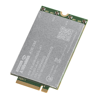
- Page 59 Structure Specifications 6.1. Product Appearance Figure 6-1 Module appearance...
- Page 60 6.2. Structural Dimensions The structural dimensions of the AIW-356 DQ-JK1 module are shown in Figure 6-2: Figure 6-2 Structural dimensions...
- Page 61 6.3. M.2 Interface Model The AIW-356 DQ-JK1 M.2 module adopts 75-pin gold finger as external interface, where 67 pins are signal pins and 8 pins are notch pins as shown in Figure 3-1. Based on the M.2 interface definition, AIW-356 DQ-JK1 module adopts Type 3052-S3-B interface (30mm × 52mm, maximum component thickness on the top is 1.5mm, PCB thickness is 0.8mm, and KEY ID is B).
- Page 62 6.5. Storage life Storage Conditions (recommended): Temperature is 23±5ºC, relative humidity less than RH 60%. Storage period: Under the recommended storage conditions, the storage life is 12 months. 6.6. Package AIW-356 DQ-JK1 module uses the tray sealed package, combined with the outer packing method using the hard cartoon box, the modules can be protected to the greatest extent during storage, transportation and use.
Need help?
Do you have a question about the AIWireless AIW-356 DQ-JK1 and is the answer not in the manual?
Questions and answers