Table of Contents
Advertisement
Quick Links
Advertisement
Table of Contents

Related Manuals for Advantech AIW-357 DK-G1P


Summary of Contents for Advantech AIW-357 DK-G1P
- Page 1 AIW-357 DK-G1P User Manual...
-
Page 2: Applicability Type
Applicability Type AIW PN Description MediaTek T700 NR SUB6/LTE FDD/LTE TDD/WCDMA M.2 3052 module B key, W/O SIM holder; w/o voice function; Only PCIe AIW-357 DK-G1P XS5G03-GBO communication interface, for USA, Europe, Japan and Taiwan region... -
Page 3: Revision History
Revision History Version Date Description V1.0 2023-06-07 First issue V1.1 2023-07-10 Section 2.10 edit LED Signal picture Add Section 2.1 pin map schematic Add Section 5.1 Product picture V1.2 2023-08-23 Add Section 2.6.1~2.6.3 USIM N.C./ N.O. description... -
Page 4: Function Overview
Thermal solutions are necessary to be put on module, so that module can work smoothly in operating temperature range. For example, thermal pad, heat sink, fan. 1.2 Product Specification and Frequency Bands AIW-357 DK-G1P is standard version with GPS function. Cellular Item... -
Page 5: Circuit Block Diagram
Model AIW-357 DK-G1P LTE Category Cat 12 B1/2/3/4/5/7/8/12/13/14/17/18/19/20/25/26/ LTE Bands 28/29/30/32/34/38/39/40/41/42/43/46/48/66/71 4G LTE DL CA 4x4 MIMO, 3CC UL CA UMTS/ Bands B1/2/4/5/8 WCDMA UL 2x2 MIMO GPS/GLONASS/BeiDou/ Galileo Frequency Band L1 Table 1-2 Product Specification and Frequency Bands 1.3 Circuit Block Diagram The circuit block diagram is shown in Figure 1-1. - Page 6 Figure 1-1 Circuit block diagram of the module...
-
Page 7: Description Of The Application Interfaces
1.4 Application Interface Features Description External Power Supply: DC 3.3V Typical PCIe Interface: PCIE3.0 1L × 1 Audio Interface: I2S x 1 I2C Interface: I2C × 1 USIM Interface: USIM × 1, eSIM x 1 (optional) RF Ipex4 connector: RF Ipex4 connector × 4 Table 1-3 Application Interface 2 Description of the Application Interfaces 2.1 M.2 Key B Interface... - Page 8 Pin No. AIW-357 DK-G1P M.2 module uses standard key B interface Pin No. +3.3V CONFIG_2 (GND) +3.3V VIO_CFG +3.3V CONFIG_1 (GND) SIM Detect (I) (1.8V) RESET# (I) (1.8V) COEX1 (IO) (1.8V) ANTCTL3 (O) (1.8V) COEX2 (IO) (1.8V) ANTCTL2 (O) (1.8V) COEX3 (IO) (1.8V)
- Page 9 Notch Notch Notch Notch Notch Notch LED1# (O) (3.3V) W_DISABLE1# (I) (3.3/1.8V) FULL_CARD_POWER_OFF# (I) (3.3/1.8V) +3.3V +3.3V CONFIG_3 (NC) Figure 2-1 AIW-357 DK-G1P Pin Map...
- Page 10 Pin Pin Name Description Voltage Type Setting vale: NC The interface of AIW-357 DK-G1P CONFIG_3 module is configured as the WWAN – PCIe Gen3, +3.3V Power supply for Module 3.135-3.63V Module ground pin +3.3V Power supply for Module 3.135-3.63V Module ground pin FULL_CARD Pull high to 1.4V~module input...
- Page 11 Pin Pin Name Description Voltage Type I2S0_BCK I2S interface 1.8V Setting vale: GND The interface of AIW-357 DK-G1P CONFIG_0 module is configured as the WWAN – PCIe Gen3, USB3.1 Gen1 I2S0_DI I2S interface 1.8V Used to wake the platform by the WWAN WOWWAN# 1.8V...
- Page 12 Pin Pin Name Description Voltage Type No connection pin Module ground pin I2C_SCL I2C clock 1.8V PETn0 PCIE interface 1.8V I2C_SDA I2C data 1.8V PETp0 PCIE interface 1.8V I2C_IRQ# I2C interrupt request 1.8V Module ground pin No connection pin PERn0 PCIE interface 1.8V No connection pin...
- Page 13 USIM1 card detect pin 1.8V RESET# Module reset input pin 1.8V No connection pin Setting vale: GND The interface of AIW-357 DK-G1P CONFIG_1 module is configured as the WWAN – PCIe Gen3, USB3.1 Gen1 +3.3V Power supply for Module 3.135-3.63V Module ground pin +3.3V...
- Page 14 Note: P indicates power pins; PI indicates input power pins; PO indicates output power pins; AI indicates pins for analog signal input; AO indicates pins for analog signal output; AIO indicates pins analog bidirectional, DI indicates pins for digital signal input; DO indicates pins for digital signal output;...
-
Page 15: Power Interface
2.2 Power Interface +3.3V pins (pin 2,4,70,72,74) are the power supply for the module The recommended +3.3V power supply circuit is shown in the figure blow: Figure 2-2 power supply recommend circuit When power source voltage lower than 3.135V, the module may shutdown or restart. The +3.3V power supply range of the module is from 3.135 V to 3.63 V. - Page 16 The following figure shows the voltage drop during Tx burst transmission Figure 2-3 power voltage lower than 3.135V The power consumption data of AIW-357 DK-G1P module under 3.3V power supply is 2.26A (Max.). Input power (V) Current avg (A) Current max (A) Condition 0.50...
- Page 17 2.3 Control Signal Interface Pin 6 FULL_CARD_POWER_OFF# FULL_CARD_POWER_OFF# Pin Function: When module off, pull high this pin then the Module booting FULL_CARD_POWER_OFF# =0→1: PMIC inside the module sequence power on FULL_CARD_POWER_OFF# =1 →0: PMIC inside the module sequence power off ...
- Page 18 Pin 67 RESET# RESET# Function: The RESET# pin is hardware reset pin used to reset the system of module. Active Low PU current: 5uA VIH: 1.45V VIL: 0.3V De-bounce time: ≤0.25ms Layout notice RESET# need to keep far from noise trace. If it is possible, please adding “GND” shielding to avoid noise coupled.
- Page 19 2.3.1. M .2 Module Timing Note 2.3.1.1. Normal Boot Figure 2-6 Normal boot module timing 2.3.1.2. Reboot (Power off Power on) Figure 2-7 Reboot module timing...
-
Page 20: Pcie Interface
2.4 PCIE Interface The blow table is PCIe interface pin definition: Pin Pin Name Pad Type Description Type. (V) PETn0 PCIE Tx - PETp0 PCIE Tx + PERn0 PCIE Rx- PERp0 PCIE Rx+ REFCLKN PCIE Reference Clock - REFCLKP PCIE Reference Clock + PCIe Reset is a functional reset to the card PERST# as defined by the PCI Express Base... - Page 21 PCIe-based Key B and Key B-M Adapters when biased from a locally generated 1.8 V voltage on the Adapter. Adapters based on a locally generated 1.8 V must be 3.3 V tolerant for such sideband signaling. Platforms that expect 1.8 V sideband signaling must protect themselves from legacy 3.3 V adapters.
- Page 22 2.4.1. PCIE Layout Notice The characteristic impedance must be implemented in PCB layout. The characteristic impedance recommends 85 +/-10% Ohm. Pin 41 PETn0 / Pin 43 PETp0 Pin 47 PERn0 / Pin 49 PERp0 The characteristic impedance recommends 100+/-20% Ohm. ...
-
Page 23: Usim Interface
2.5 I2C Interface AIW-357 DK-G1P module provides I2C interface. The I2C interface is open drain and requires external PU to 1.8 V. Pin No Pin Name Pad Type Description Typ. (V) I2C_SCL I2C clock I2C_SDA I2C data I2C_IRQ# I2C interrupt request Table 2-6 I2C interface 2.6 USIM Interface... - Page 24 2.6.1. N.C. (Normally Closed) SIM card Slot The reference circuit design for N.C. (Normally Closed) SIM card slot is shown in Figure 2-8: Figure 2-8. Ref. SIM Card Connector Schematic (Normally Closed SIM card slot) The principles of the N.C.SIM card slot are described as follows: ...
- Page 25 2.6.2. N.O. (Normally Open) SIM card Slot The reference circuit design for N.C. (Normally Open) SIM card slot is shown in Figure 2-9: Figure 2-9. Ref. SIM Card Connector Schematic (Normally Open SIM card slot, Recommended use) The principles of the N.C.SIM card slot are described as follows: ...
- Page 26 2.6.3. SIM Card connector layout Notice: (1) Place the ESD protection device near the corresponding pin. If an RC filter is required, place it on the appropriate ESD-protected device. (2) Isolate the SIM card signal from other high-speed signals to prevent the signal from receiving speed signals that are highly affected by the SIM card.
- Page 27 Table 2-8 I2S interface 2.8 RF Interface AIW-357 DK-G1P module use 4 ipex-4 RF connectors to connect external antenna. Connector “M” is for main antenna connection, used to transmit and receive and RF signals. Connector “D/G” is for Diversity antenna connection, used to receive the diversity RF signals and L1 GNSS signal (optional).
- Page 28 Default Tx Port WCDMA Ant0 Band: B1, B3, B4, B5, B8 Ant0 Band: B1, B2, B3, B4, B5, B7, B8, B12, B13, B14, B17, B18, B19, B20, B25, B26, B28, B30, B34, B38, B39, B40, B41, B66, B71 ...
- Page 29 WCDMA Ant0 PRx Band: B1, B3, B4, B5, B8 Ant2 DRx Band: B1, B3, B4 Ant3 DRx Band: B5, B8 Ant0 PRx Band: B1, B2, B3, B4, B5, B7, B8, B12, B13, B14, B17, B18, B19, B20, B25, B26, B28, B29, B30, B32, B34, B38, B39, B40, B41, B46, B66, B71 DRx Band: B42, B43, B48 ...
-
Page 30: Configuration Interface
(Pin 69) (Pin 75) (Pin 1) WWAN – PCIe Table 2-10 AIW-357 DK-G1P module configuration 2.10 LED Signal Pin 10 LED1# provide LED current sink channels for general LED indicator application. LED1# supports up to 12mA and dropout voltage ≤ 225mV. - Page 31 3 RF Specifications 3.1 Operation Frequency 3.1.1. NR Operating Frequencies Uplink (UL) operating band Downlink (DL) operating operating Duplex Mode – F – F band F UL_low UL_high DL_low DL_high band 1920 MHz – 1980 MHz 2110 MHz – 2170 MHz 1850 MHz –...
- Page 32 3.1.2. LTE Operating Frequencies Downlink (DL) operating E-UTRA Uplink (UL) operating band band Operating Duplex Mode Band – F – F UL_low UL_high DL_low DL_high 1920 MHz – 1980 MHz 2110 MHz – 2170 MHz 1850 MHz – 1910 MHz 1930 MHz –...
- Page 33 Downlink (DL) operating E-UTRA Uplink (UL) operating band band Operating Duplex Mode Band – F – F UL_low UL_high DL_low DL_high 2010 MHz – 2025 MHz 2010 MHz – 2025 MHz 2570 MHz – 2620 MHz 2570 MHz – 2620 MHz 1880 MHz –...
-
Page 34: Operating Band
Table 3-3 UTRA/FDD is designed to operate in either of the following paired bands 3.2 Operating Band AIW-357 DK-G1P Band n1/2/3/5/7/8/20/25/28/30 NR Band /38/40/41/48/66/71/77/78/79 NR CA ENDC B1/2/3/4/5/7/8/12/13/14/17/18/19/20/25/26/28/29 LTE Band /30/32/34/38/39/40/41/42/43/46/48/66/71 LTE CA WCDMA Band B1/2/4/5/8 Table 3-4 Operating Band for AIW-357 DK-G1P... -
Page 35: Conducted Rf Measurement
3.3 Conducted RF Measurement AIW-357 DK-G1P modules meet all 3GPP test standards relating to 3G, LTE and 5G. NR supports most main features in 3GPP Release 15 LTE supports most main features in 3GPP Release 14 3G supports most main features in 3GPP Release 7 and Release 8 3.4 Conducted RX Sensitivity... - Page 36 3.4.1. NR Conducted RX sensitivity 3GPP QPSK Design Duplex Bandwidth Prefsens Spec. NR Band Mode (KHz) (MHz) (dBm) (dBm) SIMO *2 SIMO *1 -97.1 -95.1 -94.1 -95.1 -101 -95.1 -97.5 -94.1 -101 -94.1 -101 -93.6 -95.6 -101.5 -97.1 -98.6 -97.1 -97.2 -95.1 -84.7...
- Page 37 3GPP QPSK Design Duplex Bandwidth Prefsens Spec. NR Band Mode (KHz) (MHz) (dBm) (dBm) SIMO *2 SIMO *1 -89.7 -91.6 -85.6 Table 3-5 NR Conducted RX sensitivity Note: SIMO is a smart antenna technology that uses a single antenna at the transmitter side and two antennas at the receiver side, which improves the RX performance.
- Page 38 3.4.2. LTE Conducted RX sensitivity 3GPP QPSK Design Spec. Bandwidth LTE Band Duplex Mode Prefsens (dBm) (MHz) (dBm) SIMO *2 SIMO *1 -103 -103 -103 -103 -102.5 -101.5 -102 -102 -102.5 -102.5 -102.5 -102.5 -102 -103 -93.5 -103 -94.5 -102 -95.5 -102 -101.5...
- Page 39 3GPP QPSK Design Spec. Bandwidth LTE Band Duplex Mode Prefsens (dBm) (MHz) SIMO *2 SIMO *1 -103 -101.5 -103.5 -102 -101.5 -103.5 -103.5 -103 Table 3-6 LTE Conducted RX sensitivity Note: SIMO is a smart antenna technology that uses a single antenna at the transmitter side and two antennas at the receiver side, which improves the RX performance.
- Page 40 3.4.3. WCDMA Conducted RX sensitivity Cell Power 3GPP Protocol Claim Band Channel Design Spec. (dBm) SIMO (dBm) SIMO *1 < –106.7 9613 -107.8 < –106.7 9750 -108.7 < –106.7 9887 -107.9 < –104.7 9263 -107.4 < –104.7 9400 -108.7 < –104.7 9537 -107.3 <...
-
Page 41: Conducted Transmit Power
3.5 Conducted Transmit Power The conducted transmit power is another indicator of the performance of the module and refers to the maximum power that the module tested at the antenna port can transmit. According to the 3GPP protocol, the required transmit power varies with the power class. Table 3-3 list the required range of the conducted transmit power of the module under 3.3 V +10% -5% voltage and normal temperature. - Page 42 Design Spec.(dBm) 5GNR 3GPP Standard (Sub 6G) (dBm) Max. Typ. Min. 23+/-2 n41(HPUE) 26+2/-3 24~26 23+2/-3 22.5 23+/-2 23+2/-2.5 20.5 23+2/-3 n77(HPUE) 26+2/-3 23+2/-3 n78(HPUE) 26+2/-3 24~26 23+2/-3 n79(HPUE) 26+2/-3 24~26 Table 3-9 NR Conducted Maximum TX sensitivity Note: n41, n77, n78, n79 support HPUE power class 2.
- Page 43 3.5.1.2. Maximum power reduction (MPR) for power class 2 of SA Maximum power reduction (MPR) for power class 2 of SA 5G NR should refer to should refer to 3GPP TS 38.101-1 V16.6.0 as below. MPR (dB) Modulation Edge RB Outer RB Inner RB allocations...
- Page 44 3.5.1.3. Maximum power reduction (MPR) for power class 3 of NSA Maximum power reduction (MPR) for power class 3 of NSA 5G NR should refer to should refer to 3GPP TS 38.101-1 V16.6.0 as below. MPR (dB) Modulation Edge RB Outer RB Inner RB allocations...
- Page 45 NOTE 2: Applicable for UE operating in FDD mode, or in TDD mode in bands other than n40, n41, n77, n78 and n79 with Pi/2 BPSK modulation and if the IE powerBoostPi2BPSK is set to 0 and if more than 40 % of slots in radio frame are used for UL transmission for bands n40, n41, n77, n78 and n79.
- Page 46 3.5.2. LTE Transmits Power 3.5.2.1. LTE Conductive Maximum Transmits Power Design Spec.(dBm) LTE Band 3GPP Standard (FDD) (dBm) Max. Typ. Min. 23+/-2 23+/-2 23+/-2 23.5 23+/-2 23.5 23+/-2 23.5 23+/-2 23+/-2 23+/-2 23.5 23+2/-2.5 20.5 23+/-2 23+/-2 23.5 23+/-2 23+/-2 23+/-2 23+/-2 23+/-2...
- Page 47 Design Spec.(dBm) LTE Band 3GPP Standard (FDD) (dBm) Max. Typ. Min. 23+/-2 23.5 23+/-2 23+/-2 23.5 23+/-2 23+/-2 22.5 23+2/-3 23+2/-3 23+2/-3 24.5 Table 3-12 LTE Conducted Maximum TX Power Note: B38, B40, B41, B42 currently set to power class 3, can support power class 2 (HPUE).
- Page 48 3.5.2.2. LTE Maximum Power Reduction (MPR) Maximum Power Reduction (MPR) and Additional Maximum Power Reduction (A-MPR) of LTE should refer to 3GPP TS 36.521-1 as below. Channel bandwidth / Transmission bandwidth (N Modulation (dB) ≤ 1 QPSK > 5 > 4 >...
- Page 49 3.6 Bandwidth Specifications 3.6.1. NR Bandwidth Specifications Channel Bandwidths (MHz) Band Mode (kHz) 90 100 20 R16*1 R16...
- Page 50 Channel Bandwidths (MHz) Band Mode (kHz) 90 100 90 100 90 100 90 100 90 100 Table 3-15 NR Bandwidth...
- Page 51 Note: The default channel bandwidth is based on 3GPP spec 38.101-1 release 15.6.0 *1 based on later spec version and need MTK library release. *2 3GPP TS 138.508-1. Test frequencies for NR operating band 40 and band 48, the channel 5MHz bandwidth can only be used as SCell.
- Page 52 3.6.2. LTE Bandwidth Specifications Duplex Channel Bandwidths (MHz) Band Mode...
- Page 53 Duplex Channel Bandwidths (MHz) Band Mode Table 3-16 LTE Bandwidth Note: B29, B32, B46 is SDL.
- Page 54 (MHz) CC number Band number Subcarrier 15K/30K spacing (Hz) Max MIMO layers per CC Modulation 256 QAM 64 QAM 256 QAM Table 3-17 LTE / NR hardware and software capability Note: AIW-357 DK-G1P only support NR UL 1 CC...
- Page 55 EN-DC 2.9 Gbps 2.97 Gbps *4 700 Mbps 530 Mbps Table 3-18 AIW-357 DK-G1P/EUI LTE / NR (SA) / ENDC maximum throughput Note: *1 120M (FDD 20M 4RX), 130M (FDD 30M 2RX) *2 Module level (actual test data in MAC).
- Page 56 3.9 RF Antenna Connector Configuration The module provides four antenna pads for connecting the external antennas. Antenna Port Function Operating Frequencies WCDMA/LTE/NR Primary TRX(SRS) 700 MHz ~ 2700 MHz ANT0 (Main) NR Diversity TRX 2496 MHz ~ 5000 MHz ANT1 MIMO (SRS) 1920 MHz ~ 5000 MHz NR Primary TRX (SRS)
- Page 57 Antenna Port Function Operating Frequencies LTE: LTE: B1, B2, B3, B4, B7, B25, B30, B1, B2, B3, B4, B7, B25, B30, B32, B38, B39, B40, B41, B42, B32, B38, B39, B40, B41, B42, B43, B46, B48, B66 B43, B46, B48, B66 ANT2 n1, n2, n3, n7, n25, n30, n38, n1, n2, n3, n7, n8, n25, n30, n38,...
-
Page 58: Antenna Connector
3.10 GPS Feature 3.10.1. Feature Supports L1 (1575.42MHz) GPS/GLONASS/Beidou/Galileo/QZSS concurrent reception GPS/Galileo only (GPS only) GPS/Galileo – GLONASS (G + G) GPS/Beidou (G + B) GPS/GLONASS/Beidou (G + G + B) GPS/Galileo/GLONASS (G + G + G) GPS/Galileo/GLONASS/Beidou (G + G + G + B) ... - Page 59 Test Result TTFF 20 times average time Cold Start 35.7 sec Warm start 32.8 sec Hot start 1.2 sec 3.10.3.2. Acquisition sensitivity Test Result Acquisition Sensitivity -145dBm 3.10.3.3. Tracking sensitivity Test Result Tracking Sensitivity -156dBm...
-
Page 60: Absolute Maximum Ratings
4 Electrical Characterisitics 4.1 Absolute Maximum Ratings Pin Name Description Min. Typ. Max. +3.3V External power supply 3.135V 3.3V Table 4-1 Absolute maximum ratings for power supply 4.2 Recommended Operating Conditions Pin Name Description Min. Typ. Max. +3.3V External power supply 3.135V 3.3V 3.63V... - Page 61 4.4 USIM DC electrical characteristics 4.4.1. USIM1_DATA USIM1_PWR=1.8V Parameter Description Min. Typ. Max. Unit Input logic low voltage Input logic high voltage 0.27 DC output logic low voltage DC output logic high voltage 0.27 Table 4-5 USIM1_data electrical characteristics ...
- Page 62 USIM1_PWR=3.0V Parameter Description Min. Typ. Max. Unit Input logic low voltage Input logic high voltage DC output logic low voltage DC output logic high voltage Table 4-8 USIM1_CLK electrical characteristics 4.4.3. USIM1_RESET USIM1_PWR=1.8V Parameter Description Min. Typ. Max. Unit Input logic low voltage Input logic high voltage...
-
Page 63: Product Appearance
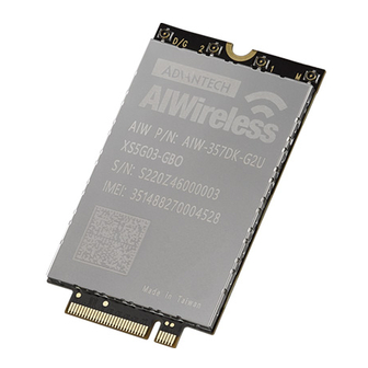
5 Process Specifications 5.1 Product Appearance Figure 5-1 Module appearance... -
Page 64: Storage Requirement
5.2 Storage Requirement The module need to be stored by sealed antistatic PE bag with the TYVEK Clay desiccant inside, under a temperature below 40°C and the relative humidity less than 60%. 5.3 Dimensions Figure 5-2 AIW-357 DK-G1P Dimensions... -
Page 65: Assembly Processes
5.4 Assembly Processes AIW-357 DK-G1P is M.2 module which follows PCI-express standard. Please follow the steps in Picture 5-2 to insert the module. Minimum two step insertion is desirable; intent is to minimize the insertion/extraction force. Step 1: As PCI-express standard, angled insertion is allowable and preferred. The recommend of angle of insertion is 20°. - Page 66 Figure 5-3 AIW-357 DK-G1P assembly processes The RF connector on AIW-357 DK-G1P module is standard MHF 4 connector, the serial number is 20579-001E manufacture by I-PEX Corporation. To prevent RF connector being damaged while install and uninstall RF cable, the recommend...
Need help?
Do you have a question about the AIW-357 DK-G1P and is the answer not in the manual?
Questions and answers